
Shagun Pal, Brijesh Kumar. Mathematical analysis of organic-pass transistor using pseudo-p-OTFTs[J]. Journal of Semiconductors, 2020, 41(6): 062601
- Journal of Semiconductors
- Vol. 41, Issue 6, 062601 (2020)
Abstract
1. Introduction
Organic electronics have attracted enormous attention in the recent years because of their advantages and compatibility with flexible electronics. An organic thin film transistor (OTFT), due to its low cost and flexible nature, finds applications in radio frequency identification (RFID) tags, sensors, digital switches, actuators, smart cards, memory circuits and Flexible display driven as backplane using OTFTs[
The most ideal conformation for the building blocks of using digital logic circuits is CMOS configuration which provide the benefits of existence of complementary technology. However, the complementary logic circuits are not quite feasible in organic TFTs because of the difference in mobility charge carrier of p- and n-type transistors, which effects the robustness of digital design. Unipolar technologies have an advantage over complementary technology because they are less complex in terms of fabrication and provide less manufacturing cost. Yet, they have a disadvantage of large area and power dissipation[
So far, these circuits were based on the steady state behavior of the logic (i.e. static logic), which is highly reliable for the flexible electronic operations. A differential logic circuit is another recent approach to analyses the issues related to static logic[
In this work, the analytical modelling of organic pass transistor has been done for the logic high and logic low. The result has been verified through calculation and simulation. Making use of this analytical model concept, the paper is sub-sectioned into four categories. The first section deals with the state of art of the work acknowledged in the field of digital circuits logic using organic thin film transistor. Additionally, the basic of dynamic logic circuit is the pass transistor, which has been studied for the logic high and low signal of the organic thin film transistor thereby making use of the basic compact model of the MOSFET. Lastly, the results are verified with the analytical work in order to study the robustness of the design for the further use in more complex digital circuitry.
2. Organic pass transistor (OPT)
The basic building block of p-type dynamic logic circuitry is the pass transistor[
For linear region,
For saturation region,
where W, L, Ci, μl, μs and Vt are channel width, channel length, gate insulator capacitance per unit area, linear mobility, saturation mobility and threshold voltage respectively. An OTFT uses an electric field to modulate the conduction of an active layer located at the interface between an insulator and organic semiconductor. Hence, it is a field effect transistor (FET) similar to the well-known metal oxide field effect transistor (MOSFET), which is a fundamental block for integrated circuits. A distinguished feature between an organic TFT (O-TFT) and MOSFET is the principle of operation; i.e., channel formation in OTFT is through accumulation process wherein MOSFET through inversion process as also reported in Refs. [18, 19]. This paper adopts the model given by Gundlach et al.[
where µlin and µsat is the linear and saturation field effect mobility of the organic device. The parameter γ has been expressed in Eq. 3(b)
To is the characteristic temperature around the Fermi level of the inorganic semiconductor and is valid for the equation T < To. For organic semiconductor, γ is always greater than 1 and has been reported around 1.1.
The field effect mobility for the linear region is derived from the trans-conductance gm and is given as in Eq. (4)
and the mobility in saturation region is calculated from Eq. (3) which is as follows:
These equations work on the assumptions of constant mobility and ignore the dependence of gate voltage on mobility of organic transistors[
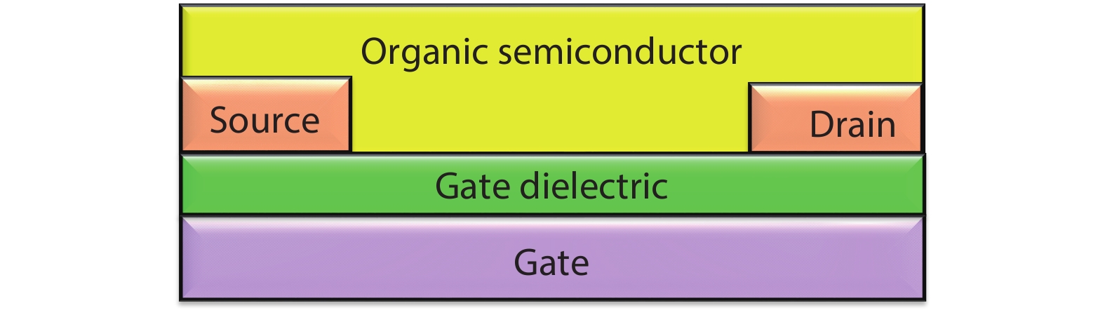
2.1. Device structure
OTFTs can be categorized as single gate and dual gate organic devices. A single gate transistor comprising of organic semiconductor as an active channel can be further categorized as the bottom contact and top contact, depending upon the position of the electrode. This paper adopts bottom gate bottom contact single gate OTFT, shown in Fig. 1 and, the device parameters from Ref. [9], as listed in Table 1.
![]()
Figure 1.(Color online) Schematic representation of the bottom gate bottom contact organic thin film transistor.
Table Infomation Is Not Enable2.2. Simulation study
The ATLAS (Silvaco) tool has made an excellent effort to study the device physics and behavior of organic thin film transistor using the Poole Frenkel mobility model[
where μ(E), E and μ0 denotes field dependent mobility, electric field, and null field mobility respectively. These, including γ, are the fitting parameters which are taken into effect for the simulation result and the mobility model. Δ and β are defined as the energy of activation and Poole-Frenkel hole aspect correspondingly. The Poole-Frenkel mobility model describes the conduction mechanism of the trap carrier owing to the electric field thermal excitation at the interface. Thermal disorder leads to charge carrier localization around the trap region thereby reducing the drain current (Ids) at low field region.
The ATLAS simulation process typically consists of three different modes: 1) structural and geometrical description, 2) physical device models and 3) defining material properties, defects and device operating conditions. In the simulation process, the defined mobility model necessitates the calculation by considering the mesh analysis at each individual region, comprising of complex triangular grids. Henceforth, a high degree of accuracy depends upon the high degree of density of meshing. This simulator gives insight into the underlying microscopic mechanism of materials along with precise monitoring of the device dimensions[
![]()
Figure 2.(Color online) Schematic representation of the mixed mode analysis of ATLAS for circuit implementation.
2.3. Device characterization and parameter extraction
The electrical characterization including output as well as transfer characteristics is drawn in Figs. 3(a) and 3(b), respectively. The Id–Vd curve in Fig. 3(a) shows the constant saturation variation suggesting a low device resistance while Fig. 3(b) shows the transfer characteristics analysis regarding behavior associated with the model at around the threshold voltage regime. The device parameters are extracted through simulation and validated with the experimental results as summarized in Table 2. These parameters show close proximity with the experimented work.
![]()
Figure 3.(Color online) Experimental[
To show the linear and saturation characteristics using MATLAB, Table 3 shows the fitting parameter that is used to model the device for the validity and Fig. 4 shows the comparative analysis of the model[
![]()
Figure 4.(Color online) Transfer characteristics curve validity of simulated device through model[
3. Analytical modelling of OPT
Previously reported work shows that logic gates are the essential block for digital and complex analog circuits. This section shows the basic working study of organic pass transistor for both the logics: high and low.
3.1. Logic high
This design depends upon the fact that the p-type organic pass transistor is able to pass logic high signal without any problem when the clock signal (CLK) signal is active low; i.e., 0 at its gate[
Because the working of p-type OPT is considered to be converse of n-type, the proposed design is made for logic high Fig. 5(a) and logic low signal as in Fig. 6(a). In the logic high, the signal is passed through the pass transistor directly similar to the p-channel transistor in a complementary transmission gate switch. The promise of this approach is that fewer transistors are required to implement any function. In the following, we first examine the analytical model for charge up event for OPT. Assume that the voltage at the Vx is initially equal to 0 i.e. Vx = 0 V at t = 0. A logic high is given to the input terminal which corresponds to Vin = VDD.
![]()
Figure 5.(Color online) (a) The basic circuitry for logic high organic-PT. (b) Variation of output voltage with respect to time through MATLAB. (c) Simulation result for the logic high signal with the input supply of 5 V.
![]()
Figure 6.(Color online) (a) The basic circuitry for logic low organic-PT. (b) working principle of the proposed model for logic low signal. (c) Variation of output voltage with respect to time through MAT Lab. (d) Simulation result for the logic low signal with the input supply of 5 V.
For the transistor T1, Vgs = 0 and Vds = Vdd = –VDD. Thus, T1 is in saturation region and hence Cx will charge up to the value given as:
Integrating Eq. (5), we get
Integrating Eq. (6), we get
Taking antilog on both sides and considering saturation time as t we get:
Solving the above, we get:
The variation of the node voltage given by Eq. (10) is graphically shown in Fig. 5(b) with respect to time. The value rises and reaches the maximum value of VDD–Vtp. Table 4 shows the comparative study between the simulated and analytical parameters for the logic high transfer signal. Fig. 5(c) shows the simulated transient behavior of the design for the time period of 4 ms. When the clock is high at the gate, the OPT is off and the input is low (i.e. Vgs= 0 then Vds= VDD= 5 V) and hence T1 transistor is in saturation and the analytical value from Eq. (10) is 2.89 V.
The analytical value is very much in close approximation of the simulation results and is derived from Eq. (10) which is tried to fit through MATLAB as shown in Fig. 5(b). The variation in the result is because the iteration process is done through Newton Raphson (NR) algorithm of ATLAS 2-D simulator. This algorithm is used in the transient state as well as steady state analysis. Moreover, in this work the full newton Raphson algorithm is used for the transient sate analysis.
3.2. Logic low
Previous work has shown that the pass transistor made using p-channel and n-channel for digital logic signals were operated using complementary clock signal at the gate in order to switch the transition from high to low, and vice versa[
As p-channel device is considered to be a strong pull up as they are able to pass logic high signal discussed above. However, they are considered weak pull down because they are not able to pass logic low signal. Henceforth, in this work a new circuitry is proposed for the logic low. This circuitry is made using two inverters and one pass transistor as in Fig. 6(a). The transistor sizing used for the inverter circuits used for the organic pass transistor is listed in Table 5.
In order to provide the path for the discharging at the output, the biased load design has been implemented which make use of external bias voltage Vbias. The analytical study of this proposed design is done and verified by the simulation as shown in Fig. 6(c) through MATLAB and Fig. 6(d) respectively.
Consider Fig. 6(b), the circuitry is made using biased-load design. For the transistor T3,
T3 is working in the linear region.
where
Putting
Solving by the method of partial fractions we get
Taking antilog on both sides of Eq. (19), we get
On expanding the series of (1 – x)–1= 1 + x+ x2…. and neglecting the higher order terms in Eq. (22) we get:
Finally, the variation of Eq. (23) is plotted as a function of time in ms in Fig. 6(c). Table 6 shows the comparative study between the simulated and analytical parameters for the logic low transfer signal.
If the node voltage goes higher than VDSAT, the organic pass transistor starts operating in linear mode and discharging of the parasitic capacitance takes place through calculating the fall time expression and hence the following study is done to measure it. For the transistor T3, Vgs = 0, Vds= –VDD then T3 is working in the linear region.
Putting
Solving by the method of partial fractions we get
Using
The variation of new constant S can be analyzed by keeping this value in Eq. (1) of the drain current equation of organic thin film transistor in linear region. We find that Ids is inversely proportional to S as given as in Eq. (33):
Thus, it is inferred that S is directly proportional to the length of the channel. Since, the channel length is dependent on the gate voltage hence it is also proportional to it. On calculating the unit of S, we found it is cm2/V2 which is the inverse of the square unit of energy of the channel. Hence channel length needs to be smaller in order to have strong energy variation.
4. Conclusion
In this paper, the mathematical model for the organic all p-type pass transistor (OPT) based on compact DC model of MOSFET is discussed. To validate the result, the OPT has been verified through analytical model using MATLAB. It was found that the simulated and the analytical parameters are very much in agreement to each other for the logic high and logic low level. This modelling will be helpful in designing dynamic logic circuits based on organic thin film transistors.
References
[1]
[2] B Kumar, B K Kaushik, Y S Negi et al. Perspectives and challenges for organic thin film transistors: Materials, devices, processes and applications. J Mater Sci: Mater Electron, 25, 1(2014).
[3] B Kumar, B K Kaushik, Y S Negi et al. Organic thin film transistors characteristics parameters, structures and their applications. Recent Advances in Intelligent Computational Systems (RAICS), 706(2011).
[4] B Kumar, B K Kaushik, Y S Negi et al. Organic thin film transistors: Structures, models, materials, fabrication, and applications: A review. Polym Rev, 54, 33(2014).
[5] D Bode, C Rolin, S Schols et al. Noise-margin analysis for organic thin-film complementary technology. IEEE Trans Electron Devices, 57, 201(2010).
[6] B Kumar, B K Kaushik, Y S Negi et al. Static and dynamic analysis of organic and hybrid inverter circuits. J Comput Electron, 12, 765(2013).
[7] T C Huang, K Fukuda, C M Lo et al. Pseudo-CMOS: A design style for low-cost and robust flexible electronics. IEEE Trans Electron Devices, 58, 141(2011).
[8] M Kimura, D Sawamoto, T Matsuda et al. Pseudo-CMOS circuits using amorphous In–Sn–Zn–O thin-film transistors. Dig Tech Pap - SID Int Symp, 45, 960(2014).
[9] B Kumar, B K Kaushik, Y S Negi et al. Single and dual gate OTFT based robust organic digital design. Microelectron Reliab, 54, 100(2014).
[10] M Venturelli, F Torricelli, M Ghittorelli et al. Unipolar differential logic for large-scale integration of flexible a-IGZO circuits. IEEE Trans Circuits Syst II, 64, 565(2017).
[11] K Myny. The development of flexible integrated circuits based on thin-film transistors. Nat Electron, 1, 30(2018).
[12] J S Kim, J H Jang, Y D Kim et al. Dynamic logic circuits using a-IGZO TFTs. IEEE Trans Electron Devices, 64, 4123(2017).
[13] M Elsobky, M Elattar, G Alavi et al. A digital library for a flexible low-voltage organic thin-film transistor technology. Org Electron Phys Mater Appl, 50, 491(2017).
[14]
[15] B Kumar, B K Kaushik, Y S Negi et al. Modeling of top and bottom contact structure organic field effect transistors. J Vac Sci Technol B, 31, 012401(2013).
[16] B Kumar, B K Kaushik, Y S Negi et al. Analytical modeling and parameter extraction of top and bottom contact structures of organic thin film transistors. Microelectron J, 44, 736(2013).
[17]
[18] P Mittal, B Kumar, Y S Negi et al. Channel length variation effect on performance parameters of organic field effect transistors. Microelectronics J, 43, 985(2012).
[19] O Marinov, M J Deen, U Zschieschang et al. Organic thin-film transistors: Part I—Compact DC modelling. IEEE Trans Electron Devices, 56, 2952(2009).
[20] D J Gundlach, L Zhou, J A Nichols et al. An experimental study of contact effects in organic thin film transistors. J Appl Phys, 100, 024509(2006).
[21] M C Hamilton, S Martin, J Kanicki. Field-effect mobility of organic polymer thin-film transistors. Chem Mater, 16, 4699(2004).
[22] D Gupta, M Katiyar, D Gupta et al. Mobility estimation incorporating the effects of contact resistance and gate voltage dependent mobility in top contact organic thin film transistors. Proc of ASID, 6(2006).
[23]
[24] P Mittal, Y S Negi, R K Singh. Impact of source and drain contact thickness on the performance of organic thin film transistors. J Semicond, 35, 124002(2014).
[25]
[26] R Escoffier, W Fichtner, D Fokkema et al. DESSIS 10.0 manual. ISE Integr Syst Eng AG: CH-Zürich, 96, 161(1996).

Set citation alerts for the article
Please enter your email address
© Copyright 2018-2021 | Chinese Laser Press. All Rights Reserved 沪ICP备15018463号-20