• Journal of Semiconductors
  • Vol. 42, Issue 2, 024101 (2021)
Zhaowu Tang1, Chunsen Liu1、2, Senfeng Zeng1, Xiaohe Huang1, Liwei Liu1, Jiayi Li1, Yugang Jiang2, David Wei Zhang1, and Peng Zhou1
Author Affiliations
  • 1State Key Laboratory of ASIC and System, School of Microelectronics, Fudan University, Shanghai 200433, China
  • 2School of Computer Science, Fudan University, Shanghai 200433, China
  • show less
    DOI: 10.1088/1674-4926/42/2/024101 Cite this Article
    Zhaowu Tang, Chunsen Liu, Senfeng Zeng, Xiaohe Huang, Liwei Liu, Jiayi Li, Yugang Jiang, David Wei Zhang, Peng Zhou. Enhancement of refresh time in quasi-nonvolatile memory by the density of states engineering[J]. Journal of Semiconductors, 2021, 42(2): 024101 Copy Citation Text show less
    (Color online) The schematic and characterization of the QNV memory. (a) The linearly varied density of states DOS(E), super-exponentially decreased electron density n(E) with the energy of Gr Dirac material, and the cut-off of electron injection from Gr Dirac material to channel over the bulk barrier ϕB. The orange dashed line in n(E) represents the Boltzmann distribution. (b) The schematic structure of the QNV memory in which MoS2 serves as the channel, Gr-hBN servers as the semi-blocking layer, and WSe2 serves as the floating gate. (c) The false-colored optical microscope image of the device. The scale bar is 5 μm. (d) The Raman spectra of monolayer Gr and multilayer MoS2 and WSe2 were measured by using a 532 nm solid-state laser. (e) The double sweep transfer characteristic of the QNV memory under VDS = 0.5 V. A large Ion/Ioff exceeding 104 is achieved when reading at VG = 0 V. The inset is the full measurement range (VG varying from –2 to 2 V) of transfer characteristics on a logarithmic scale.
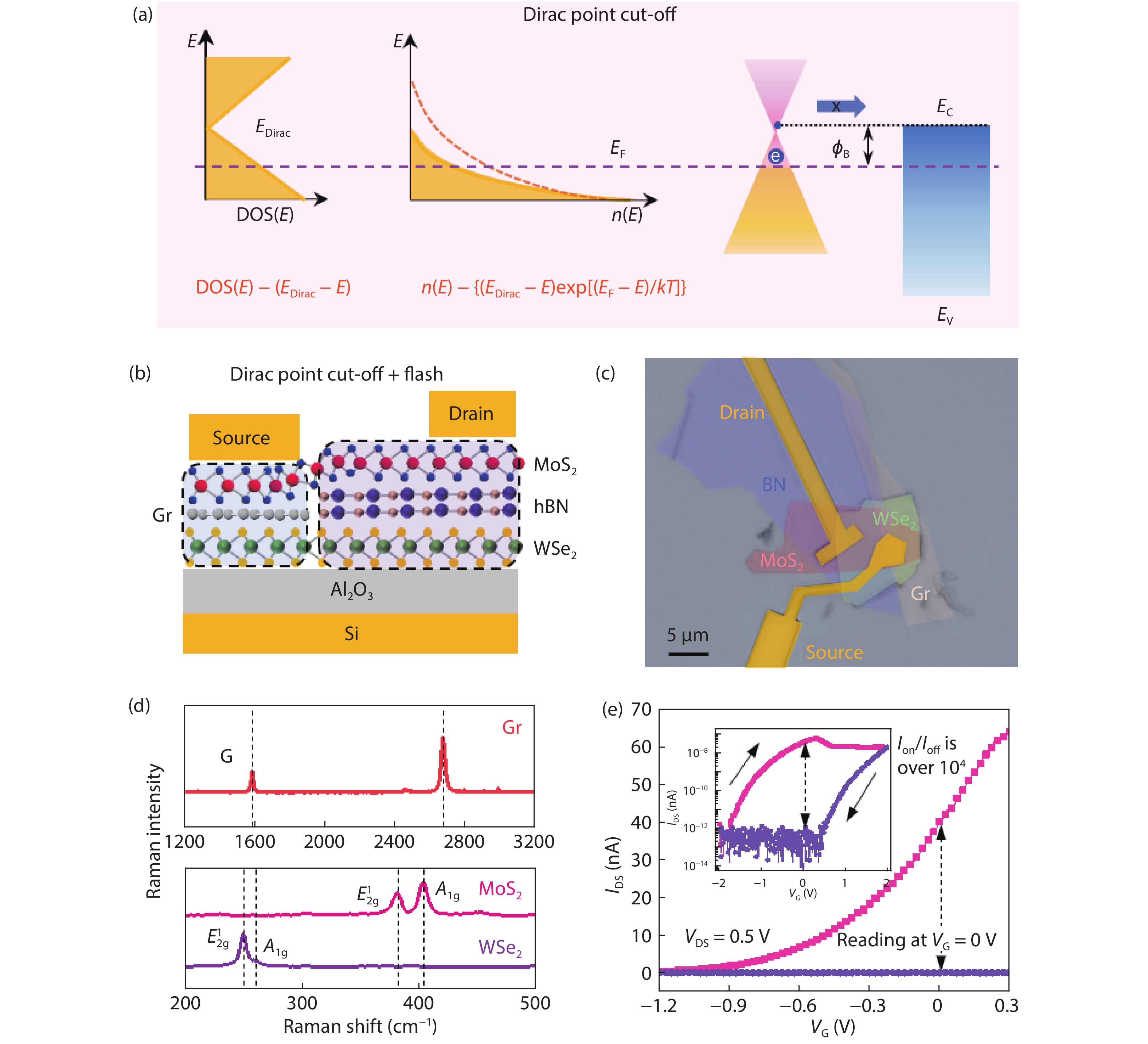
    Fig. 1. (Color online) The schematic and characterization of the QNV memory. (a) The linearly varied density of states DOS(E), super-exponentially decreased electron density n(E) with the energy of Gr Dirac material, and the cut-off of electron injection from Gr Dirac material to channel over the bulk barrier ϕB. The orange dashed line in n(E) represents the Boltzmann distribution. (b) The schematic structure of the QNV memory in which MoS2 serves as the channel, Gr-hBN servers as the semi-blocking layer, and WSe2 serves as the floating gate. (c) The false-colored optical microscope image of the device. The scale bar is 5 μm. (d) The Raman spectra of monolayer Gr and multilayer MoS2 and WSe2 were measured by using a 532 nm solid-state laser. (e) The double sweep transfer characteristic of the QNV memory under VDS = 0.5 V. A large Ion/Ioff exceeding 104 is achieved when reading at VG = 0 V. The inset is the full measurement range (VG varying from –2 to 2 V) of transfer characteristics on a logarithmic scale.
    (Color online) The symmetric ultrafast programming and erasing operation of the QNV memory. (a) The initial state is state-1 and the 5 V gate voltage pulse with different pulse widths is applied for the programming operation. After that, the reading operation is carried out at VG = 0 V and VDS = 0.5 V. (b) The initial state is state-0 after applying a positive gate voltage pulse for programming and the –5 V gate voltage pulse with different pulse width is applied for the erasing operation. After that the reading operation is carried out at VG = 0 V and VDS = 0.5 V. (c) The current state after the programming and erasing operations with different pulse width gate voltage pulse (the pulse amplitude is fixed 5 V). The data points of the current state are the mean value of the sampling points produced while monitoring the channel current 5 s after the programming/erasing operation. (d) The endurance of the device for 100 cycles of the programming/erasing pulse, demonstrating that no performance degradation was observed.
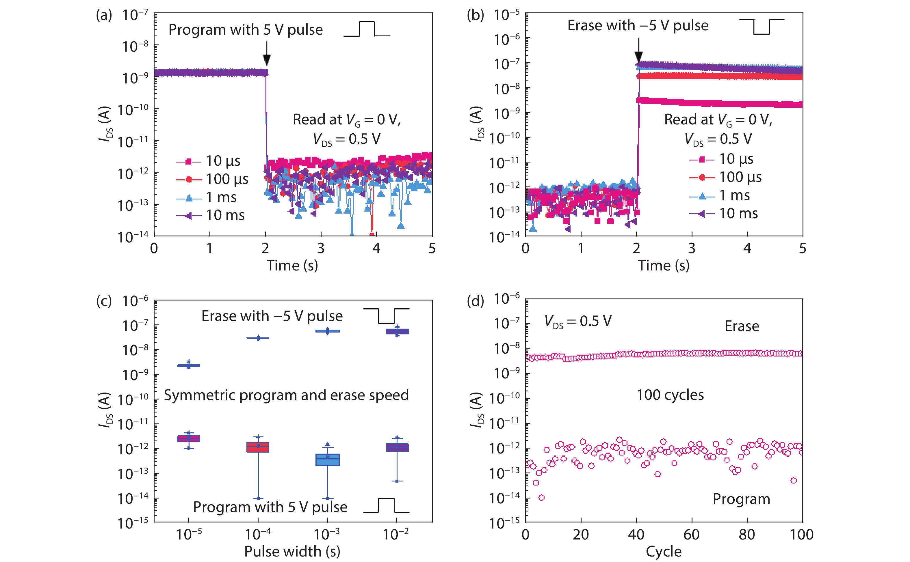
    Fig. 2. (Color online) The symmetric ultrafast programming and erasing operation of the QNV memory. (a) The initial state is state-1 and the 5 V gate voltage pulse with different pulse widths is applied for the programming operation. After that, the reading operation is carried out at VG = 0 V and VDS = 0.5 V. (b) The initial state is state-0 after applying a positive gate voltage pulse for programming and the –5 V gate voltage pulse with different pulse width is applied for the erasing operation. After that the reading operation is carried out at VG = 0 V and VDS = 0.5 V. (c) The current state after the programming and erasing operations with different pulse width gate voltage pulse (the pulse amplitude is fixed 5 V). The data points of the current state are the mean value of the sampling points produced while monitoring the channel current 5 s after the programming/erasing operation. (d) The endurance of the device for 100 cycles of the programming/erasing pulse, demonstrating that no performance degradation was observed.
    (Color online) The data retention ability of the QNV memory. (a) The retention characteristic of the memory after the programming operation with different gate pulse widths (the pulse amplitude is fixed 5 V). (b) The relationship between the state-0 output current and program pulse width for different wait times. (c) The comparison of the refresh time of our device with the other QNV memory devices[1, 18–20] under different pulse widths.
    Fig. 3. (Color online) The data retention ability of the QNV memory. (a) The retention characteristic of the memory after the programming operation with different gate pulse widths (the pulse amplitude is fixed 5 V). (b) The relationship between the state-0 output current and program pulse width for different wait times. (c) The comparison of the refresh time of our device with the other QNV memory devices[1, 1820] under different pulse widths.
    (Color online) The schematic illustrations of the band diagrams and charges transport in the QNV memory at different operation modes: (a) program, (b) read-0, (c) erase, and (d) read-1. The blue balls and arrows represent the electrons and electron flow direction, respectively. The approximate electron affinities of MoS2 and WSe2 are 4.0–4.2, 3.5–4.0 eV respectively, and the work function of monolayer Gr is ~4.3 eV.
    Fig. 4. (Color online) The schematic illustrations of the band diagrams and charges transport in the QNV memory at different operation modes: (a) program, (b) read-0, (c) erase, and (d) read-1. The blue balls and arrows represent the electrons and electron flow direction, respectively. The approximate electron affinities of MoS2 and WSe2 are 4.0–4.2, 3.5–4.0 eV respectively, and the work function of monolayer Gr is ~4.3 eV.
    Zhaowu Tang, Chunsen Liu, Senfeng Zeng, Xiaohe Huang, Liwei Liu, Jiayi Li, Yugang Jiang, David Wei Zhang, Peng Zhou. Enhancement of refresh time in quasi-nonvolatile memory by the density of states engineering[J]. Journal of Semiconductors, 2021, 42(2): 024101
    Download Citation