
Zhaowu Tang, Chunsen Liu, Senfeng Zeng, Xiaohe Huang, Liwei Liu, Jiayi Li, Yugang Jiang, David Wei Zhang, Peng Zhou. Enhancement of refresh time in quasi-nonvolatile memory by the density of states engineering[J]. Journal of Semiconductors, 2021, 42(2): 024101
- Journal of Semiconductors
- Vol. 42, Issue 2, 024101 (2021)
Abstract
1. Introduction
The existing commercial memory can be divided into two categories: volatile memory and nonvolatile memory. Volatile memory exhibits ultrafast accessing speed, but the data stored will disappear once the power is lost. Especially for dynamic random access memory (DRAM), frequent refresh is needed to retain the data. Nonvolatile memory can store data for up to 10 years without the power supply, but its accessing speed is much lower than volatile memory. To bridge the large timescale gap between volatile and non-volatile memory, the third type of memory called quasi-nonvolatile (QNV) memory has been proposed recently[
In consideration of that the limited refresh time of QNV memory is mainly caused by the leakage of high-energy electrons crossing the barrier between the channel and the floating gate through the p–n junction, a new approach to cut down the high-energy electrons needs to be adopted to extend the refresh time. Two dimensional (2D) Dirac material such as the monolayer graphene (Gr) has a linear band dispersion[
In this work, we propose and fabricate a QNV SFG memory based on the DOS engineered van der Waals heterostructures. By utilizing the SFG architecture, the device exhibits the symmetric ultrafast programming and erasing speeds of 10 μs, which is 103 times faster than that of the previously reported 2D material based conventional flash memory devices[
2. Experimental section
Firstly, the 30 nm Al2O3 layer was grown on highly p-doped Si substrates by atomic layer deposition as the back-gate dielectric. Then all of the 2D material including multilayer WSe2, hBN, MoS2, and monolayer Gr were mechanically exfoliated from bulk materials to polydimethylsiloxane (PDMS) and then were transferred in turn from the PDMS on the Al2O3/Si substrate to form the WSe2/hBN/Gr/MoS2 SFG van der Waals heterostructures. After that, Cr/Au (5 nm/30 nm) films were patterned by using electron-beam lithography and deposited by electron-beam evaporation as the source and drain electrodes. Finally, the annealing process was performed at 250 °C in a nitrogen atmosphere for 2 h to ensure good contacts between the films of the device. The corresponding optical microscope images of the device during the preparation process are shown in supplementary Fig. S1.
The Raman spectroscopy of the 2D material used in the device was measured in an SOL instrument by using a 532 nm solid-state laser. The measurement of the electrical performance of the device was performed in a probe station (Cascade Summit 11000 type) by using the Agilent B1500A semiconductor device parameter analyzer. The DC signals and the voltage pulses used in the test were generated by the source/monitor unit (SMU) and the semiconductor pulse generator unit (SPGU) of B1500A, respectively. Additionally, all the above measurements of the device were completed at room temperature in an air environment.
3. Results and discussion
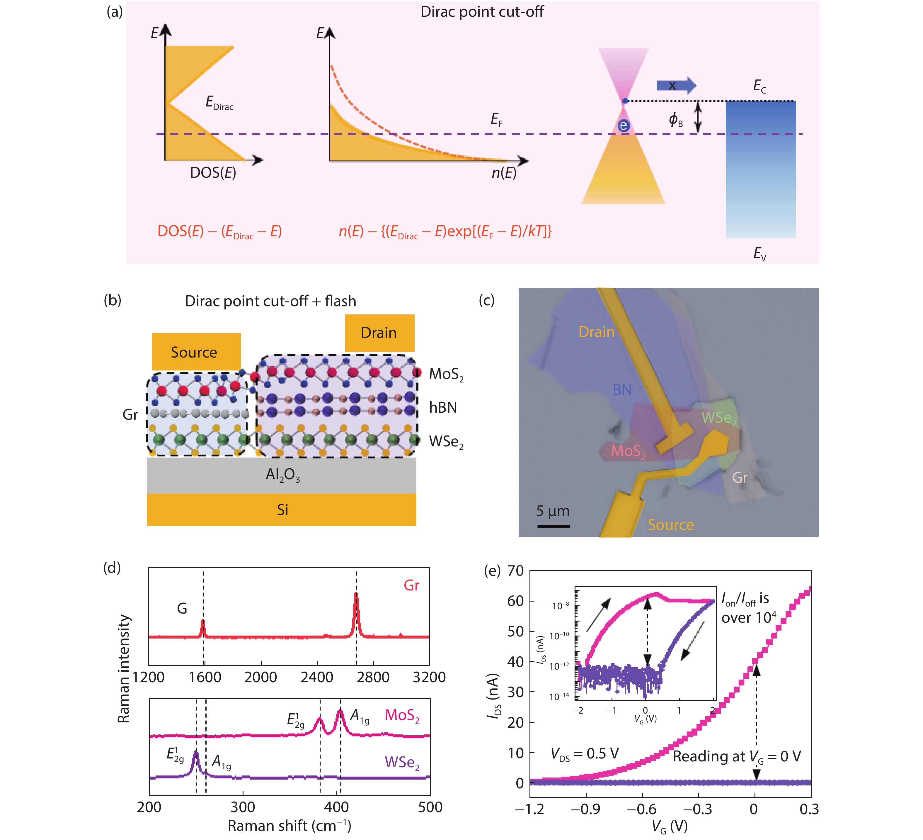
As shown in Fig. 1(a), the p-type Gr Dirac material has a linearly decreased DOS with energy [DOS(E)–(EDirac – E)] and thus its electron density n(E) above EF super-exponentially decreases with energy increasing toward the Dirac point energy (n(E)–{(EDirac – E)exp[(EF – E)/kT]}, where the k and T refer to the Boltzmann constant and temperature respectively), contributing to a more concentrated electron distribution around EF. When it is used as the electron source of an n-type channel, most electrons cannot cross the bulk barrier ϕB into the channel owing to the long thermal tail of high-energy electrons in Gr has been greatly cut down. This kind of Dirac point cut-off effect is suitable for SFG QNV memory to suppress the leakage of high-energy electrons crossing the bulk barrier ϕB between the channel and the floating gate so that its refresh time can be prolonged. Fig. 1(b) shows the schematic structure of the QNV memory where MoS2 is used as the channel, Gr-hBN is used as the semi-blocking layer and WSe2 is used as the floating gate. And the MoS2 is n-type while the Gr is p-type (as shown in supplementary Fig. S2), which satisfies the design requirements of the Dirac point cut-off effect. Besides, the silicon substrate with 30 nm Al2O3 dielectric works as the global back gate and 5/30 nm Cr/Au film was patterned and deposited on the MoS2 film as the source and drain electrode. Fig. 1(c) displays the optical microscope image of the device. The 2D crystals used in the device were characterized by Raman spectroscopy, as shown in Fig. 1(d). The Gr exhibits the G peak at ~1583.0 cm–1 and 2D peak at ~2673.9 cm–1 and the intensity ratio of 2D to G peak is ~2.56, indicating that it is a monolayer Gr[
![]()
Figure 1.(Color online) The schematic and characterization of the QNV memory. (a) The linearly varied density of states DOS(
The programming and erasing operation of the QNV memory are investigated by applying a series of gate voltage pulses with different pulse widths (10 μs, 100 μs, 1 ms, 10 ms), as presented in Fig. 2. The memory was set to state-0 and state-1 by the positive and negative gate voltage pulse respectively, and the state-0 and state-1 correspond to a high resistance state of around 500 GΩ and a relatively low resistance state of less than 500 MΩ respectively. As shown in Fig. 2(a), the initial state of the device is state-1 with a drain-source current (IDS) of around 1 nA. A series of 5 V gate voltage pulses were applied to perform the programming state-0 operation, and then VG and VDS were set to 0 and 0.5 V respectively to perform the reading operation. An output current of around 1 pA was observed, indicating that the device has been successfully set to state-0 after the 5 V programming pulse with the minimum pulse width of 10 μs. Additionally, the erasing operation of the device is presented in Fig. 2(b). Its initial state has been pre-set to state-0 after a 5 V gate voltage pulse of 100 μs, and next a series of –5 V gate voltage pulses were applied to perform the erasing operation. When reading at VG = 0 V, VDS = 0.5 V, a high output current over 1 nA was measured, indicating that the device can also be successfully erased to state-1 after the –5 V erasing pulse with the minimum pulse width of 10 μs. Fig. 2(c) summarizes the current state after the programming and erasing operations under different gate voltage pulse widths from 10 μs to 10 ms. It can be seen that all the programming and erasing operations can effectively set the device to state-0 and state-1 even if the gate voltage pulse width is reduced to as short as 10 μs, which indicates that the QNV memory can achieve the symmetric ultrafast programming and erasing speeds of 10 μs. What’s more, the endurance of the device is presented in Fig. 2(d). After 100 cycles of the programming/erasing operations, the device can still work normally without significant performance degradation.
![]()
Figure 2.(Color online) The symmetric ultrafast programming and erasing operation of the QNV memory. (a) The initial state is state-1 and the 5 V gate voltage pulse with different pulse widths is applied for the programming operation. After that, the reading operation is carried out at
Fig. 3 shows the data retention ability of the QNV memory after the programming operation with different pulse widths (10 μs, 100 μs, 1 ms, 10 ms). As shown in Fig. 3(a), due to the unavoidable leakage of electrons stored in the WSe2 floating gate through the semi-blocking layer, the channel current gradually increases with time after the gate voltage pulse is removed. And the reference state-1 refers to the initial state of the device before the programming operation. Fig. 3(b) displays the relationship between the state-0 channel current and program pulse width for different wait times (the time after the programming operation). It can be seen that the longer wait time results in the larger detected output channel current due to the gradual leakage of the storage charge. When the state-0 current is too close to the initial reference state-1, a refresh operation is needed. As shown in Fig. 3(b), even after a long wait time of 100 s, the state-0 current is still sufficiently distinguished with reference state-1 (the current ratio between state-1 and state-0 is over 10), which indicates that the refresh time of the QNV memory is more than 100 s. To more intuitively reflect the advantages of our device in refresh time, Fig. 3(c) shows the comparison of refresh time between our device and all other reported QNV memory devices[
![]()
Figure 3.(Color online) The data retention ability of the QNV memory. (a) The retention characteristic of the memory after the programming operation with different gate pulse widths (the pulse amplitude is fixed 5 V). (b) The relationship between the state-0 output current and program pulse width for different wait times. (c) The comparison of the refresh time of our device with the other QNV memory devices[
Since our QNV memory combines the Dirac point cut-off effect and the conventional flash memory technology, its mechanism can be perspicuously illustrated by the band diagrams and charges transport in the QNV memory, as shown in Fig. 4. The Gr/hBN composite semi-blocking layer determines that there are two charge transport paths in our device: one is the flash memory path in which charges tunnel through the hBN layer, and the other one is the transparent path in which charges cross through the Gr layer. For the programming operation, a 5 V voltage pulse is applied on the back gate and the electrons in the MoS2 channel cross through the hBN or Gr layer into the WSe2 floating gate, as shown in Fig. 4(a). Since the Gr path is transparent with no barrier, the electrons can be easily and quickly injected into the floating gate, which results in an ultrafast programming speed on the timescale of 10 μs. When the read-1 operation is performed at VG = 0 V and VDS = 0.5 V [Fig. 4(b)], the Dirac point cut-off effect between the n-type MoS2 and p-type Gr [see Fig. 1(a)] and the hBN blocking layer keep the electrons in the WSe2 floating gate from leaking to MoS2 channel. However, it should be noted that the thermal diffusion of high-energy electrons cannot be completely cut off, which results in non-permanent electron storage. For the erasing operation [Fig. 4(c)] with a –5 V gate voltage pulse, the electrons stored in the floating gate are injected back to the channel in the same way and thus also resulting in a symmetric ultrafast erasing speed. When the device is in the initial state-1 after the erasing operation, the electrons maintain thermal equilibrium in the MoS2/Gr/WSe2 region, and thus the charge transfer between the channel and the floating gate is a dynamic equilibrium process, as shown in Fig. 4(d).
![]()
Figure 4.(Color online) The schematic illustrations of the band diagrams and charges transport in the QNV memory at different operation modes: (a) program, (b) read-0, (c) erase, and (d) read-1. The blue balls and arrows represent the electrons and electron flow direction, respectively. The approximate electron affinities of MoS2 and WSe2 are 4.0–4.2, 3.5–4.0 eV respectively, and the work function of monolayer Gr is ~4.3 eV.
4. Conclusion
In summary, based on the SFG architecture and the DOS engineered van der Waals heterostructures, an ultrafast 2D QNV memory with a long refresh time is demonstrated. Inheriting the superiority of the SFG memory in the accessing speed, the device exhibits the symmetric ultrafast programming and erasing speeds of 10 μs. More importantly, the leakage of electrons from the floating gate to the channel is greatly suppressed by the Dirac point cut-off effect between the n-type MoS2 and p-type Gr, contributing to a long refresh time of more than 100 s that exceeds all previously reported QNV memory devices. Benefit from this significant enhancement of refresh time, considerable power consumption resulting from frequent refresh can be greatly reduced. Therefore, the novel structure in this work provides a reliable way to develop the next-generation memory device with high-speed and low-power.
Acknowledgments
This work was supported by the National Natural Science Foundation of China (61925402, 61851402 and 61734003), Science and Technology Commission of Shanghai Municipality (19JC1416600), National Key Research and Development Program (2017YFB0405600), Shanghai Education Development Foundation and Shanghai Municipal Education Commission Shuguang Program (18SG01), China Postdoctoral Science Foundation (2019M661358, 2019TQ0065).
Appendix A. Supplementary material
Supplementary data associated with this article can be found, in the online version, at https://doi.org/10.1088/1674-4926/42/2/024101.
References
[1] C Liu, X Yan, X Song et al. A semi-floating gate memory based on van der Waals heterostructures for quasi-non-volatile applications. Nat Nanotechnol, 13, 404(2018).
[2] K S Novoselov, A K Geim, S V Morozov et al. Electric field effect in atomically thin carbon films. Science, 306, 666(2004).
[3] C Qiu, F Liu, L Xu et al. Dirac-source field-effect transistors as energy-efficient, high-performance electronic switches. Science, 361, 387(2018).
[4] F Liu, C Qiu, Z Zhang et al. Dirac electrons at the source: breaking the 60-mV/decade switching limit. IEEE Trans Electron Devices, 65, 2736(2018).
[5] F Liu, C Qiu, Z Zhang et al. First principles simulation of energy efficient switching by source density of states engineering. IEEE International Electron Devices Meeting (IEDM), 33(2018).
[6] J Lyu, J Pei, Y Guo et al. A new opportunity for 2D van der Waals heterostructures: making steep-slope transistors. Adv Mater, 32, 1906000(2020).
[7] W J Yu, S H Chae, S Y Lee et al. Ultra-transparent, flexible single-walled carbon nanotube non-volatile memory device with an oxygen-decorated graphene electrode. Adv Mater, 23, 1889(2011).
[8] S Lee, E B Song, S Kim et al. Impact of gate work-function on memory characteristics in Al2O3/HfO
[9] S M Kim, E B Song, S Lee et al. Transparent and flexible graphene charge-trap memory. ACS Nano, 6, 7879(2012).
[10] S Bertolazzi, D Krasnozhon, A Kis. Nonvolatile memory cells based on MoS2/graphene heterostructures. ACS Nano, 7, 3246(2013).
[11] M S Choi, G H Lee, Y J Yu et al. Controlled charge trapping by molybdenum disulphide and graphene in ultrathin heterostructured memory devices. Nat Commun, 4, 1624(2013).
[12] E Zhang, W Wang, C Zhang et al. Tunable charge-trap memory based on few-layer MoS2. ACS Nano, 9, 612(2015).
[13] Q A Vu, Y S Shin, Y R Kim et al. Two-terminal floating-gate memory with van der Waals heterostructures for ultrahigh on/off ratio. Nat Commun, 7, 12725(2016).
[14] G He, H Ramamoorthy, C P Kwan et al. Thermally assisted nonvolatile memory in monolayer MoS2 transistors. Nano Lett, 16, 6445(2016).
[15] Y T Lee, H Kwon, J S Kim et al. Nonvolatile ferroelectric memory circuit using black phosphorus nanosheet-based field-effect transistors with P(VDF-TrFE) polymer. ACS Nano, 9, 10394(2015).
[16] X Hou, H Zhang, C Liu et al. Charge-trap memory based on hybrid 0D quantum dot-2D WSe2 structure. Small, 14, 1800319(2018).
[17] A Mishra, A Janardanan, M Khare et al. Reduced multilayer graphene oxide floating gate flash memory with large memory window and robust retention characteristics. IEEE Electron Device Lett, 34, 1136(2013).
[18] Y Ding, L Liu, J Li et al. A semi-floating memory with 535% enhancement of refresh time by local field modulation. Adv Funct Mater, 30, 1908089(2020).
[19] J Li, L Liu, X Chen et al. Symmetric ultrafast writing and erasing speeds in quasi-nonvolatile memory via van der Waals heterostructures. Adv Mater, 31, 1808035(2019).
[20] G Wu, B Tian, L Liu et al. Programmable transition metal dichalcogenide homojunctions controlled by nonvolatile ferroelectric domains. Nat Electron, 3, 43(2020).
[21] C Liu, P Zhou. Memory Devices Based on Van der Waals Heterostructures. ACS Mater Lett, 2, 1101(2020).
[22] J Liu, Z Huang, F Lai et al. Controllable growth of the graphene from millimeter-sized monolayer to multilayer on Cu by chemical vapor deposition. Nanoscale Res Lett, 10, 455(2015).
[23] G P Dai, M H Wu, D K Taylor et al. Hybrid 3D graphene and aligned carbon nanofiber array architectures. RSC Adv, 2, 8965(2012).
[24] Y Cao, Z Wang, Q Bian et al. Phonon modes and photonic excitation transitions of MoS2 induced by top-deposited graphene revealed by Raman spectroscopy and photoluminescence. Appl Phys Lett, 114, 133103(2019).
[25] S Mouri, Y Miyauchi, K Matsuda. Tunable photoluminescence of monolayer MoS2 via chemical doping. Nano Lett, 13, 5944(2013).
[26] G H Ahn, M Amani, H Rasool et al. Strain-engineered growth of two-dimensional materials. Nat Commun, 8, 608(2017).


Set citation alerts for the article
Please enter your email address

© Copyright 2018-2021 | Chinese Laser Press. All Rights Reserved 沪ICP备15018463号-20