
Hanliu Zhao, Xinghao Sun, Zhengrui Zhu, Wen Zhong, Dongdong Song, Weibing Lu, Li Tao. Physical vapor deposited 2D bismuth for CMOS technology[J]. Journal of Semiconductors, 2020, 41(8): 081001
- Journal of Semiconductors
- Vol. 41, Issue 8, 081001 (2020)
Abstract
1. Introduction
Beginning with the successful exfoliation of monolayer graphene, two-dimensional (2D) materials, including h-BN, transition metal dichalcogenides (TMDs), Xenes and MXenes, have attracted significant interest in the past dozen years due to their unique physical and chemical properties. As a specific Xene branch, 2D atomic sheets of group VA elements possess tunable electrical, thermal, optical properties compared to their bulk state, thus having a broad prospect in the field of CMOS applications, such as field-effect transistors (FET), sensors, optoelectronics, thermoelectrics, topological insulators and so on. Group VA consists of nitrogen, phosphorus, arsenic, antimony and bismuth, all of which have a puckered or buckled layered structure except for nitrogen. Black phosphorus (BP) is the most thermodynamically stable allotrope of phosphorus under standard conditions[
![]()
Figure 1.(Color online) (a) Atomic structure of α phase P (left) and
As the most intensively studied 2D Xene material, BP is known for its tunable direct band gap (0.3 eV for bulk and ~2 eV for monolayer), anisotropic transport properties, thickness-dependent anisotropic optical response[
2D monolayer arsenene possesses carrier mobility as high as 635 cm2V–1s–1 for electrons and 1700 cm2V–1 s–1for holes as calculated[
As the last element of the VA group, β-bismuth possesses the same rhombohedral structure as arsenic and antimony[
With the rapid increase in 2D materials research, many emerging 2D materials such as graphene, BP and TMDs, have been demonstrated to be applicable to CMOS devices, including transistors, memories and inverters, benefiting from their high carrier mobility or tunable bandgap[
Starting from the structure and properties of bismuth, this review summarizes various physical vapor deposition of 2D bismuth, followed by its existing or potential CMOS applications. Besides, bismuth derivatives are mentioned as a strategy to enhance the performance of 2D bismuth. Finally, a brief summary on the current challenges and future prospects are discussed. Besides, it should be noted that in this review, “bismuthene” refers to bismuth from monolayer to 4 nm, “2D bismuth” indicates 4–30 nm (critical thickness for observing quantum confinement effect[
2. Structure and properties of bismuthene
As a cousin of phosphorene, the unique structure of bismuthene gives rise to extraordinary electronic properties. To utilize the properties in potential applications, it is necessary to understand the relationship between the atomic, band structure and electronic properties of 2D bismuth.
2.1. Atomic structure
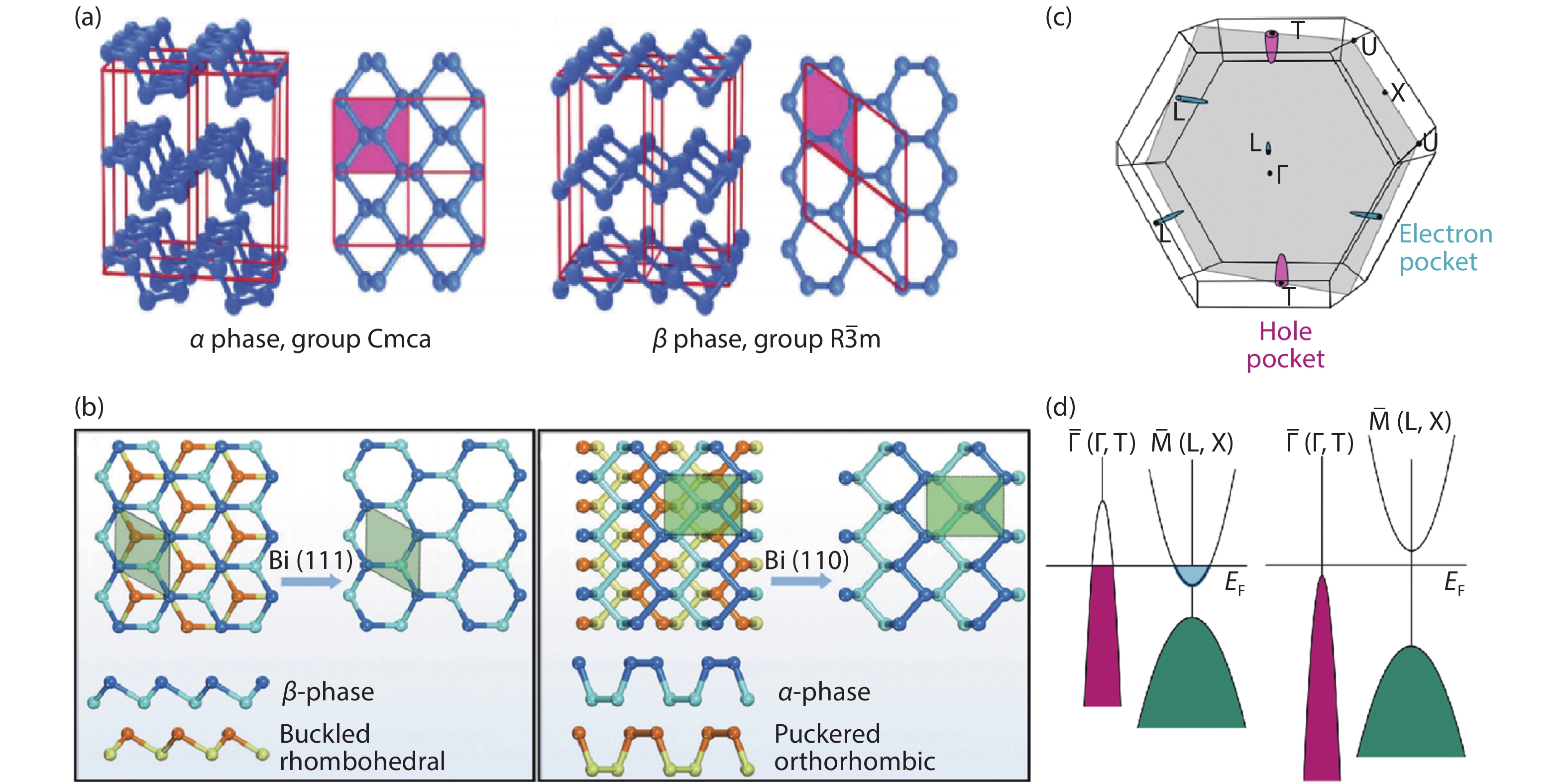
Bismuth possesses a rhombohedral A7-type structure, namely β phase as shown in Fig. 1(a), space group R
2.2. Band structure and electronic properties
Bismuth has an electron configuration of 6s2 6p3[
In general, monolayer bismuthene possesses a moderate direct bandgap ranging from 0.43 to 0.99 eV depending on different computation methods[
![]()
Figure 2.(Color online) (a) Band structure of bismuthene is calculated without (up) and with (down) the SOC. Reproduced with permission from Ref. [
Strong SOC effect leads to a splitting of the states in heavy Bi atoms, and the large energy difference between the 6p1/2 and 6p3/2 is 1.5 eV after splitting[
3. Physical vapor deposition of 2D bismuth
Material synthesis or growth is the first step to perform experimental study on the aforementioned exotic properties of bismuthene. To date, a number of methods have been developed to fabricate 2D bismuth, including physical vapor deposition, liquid exfoliation[
3.1. Molecular beam epitaxy (MBE)
Under ultra-high vacuum (~10–8 Pa) and small mismatch, atoms arrange and form high-quality single crystal films with controllable thickness, the surface being very smooth with roughness lower than 1 nm, even picometer level[
The interaction between the substrate and 2D bismuth has a crucial effect on film growth, and substrate-dependent electronic properties and orientations on various substrates are extensively studied, e.g. SiC[
![]()
Figure 3.(Color online) (a) Sketch and (b) STM image of flat honeycomb bismuthene epitaxy on SiC (0001). Reproduced with permission from Ref. [
Furthermore, Meyer et al. reported a sudden and massive generation of misfit dislocations at a critical thickness of 4 nm in Bi (111)/Si (001) for strain relaxation in Fig. 3(g)[
Nevertheless, the MBE method has a high requirement on facility with high cost and a long experimentation period, preventing it from large-scale 2D bismuth preparation.
3.2. Pulsed laser deposition (PLD)
The PLD method uses a high energy laser to vaporize and dissociate the material under 10–5–10–6 Pa. High ion energy promotes the adatom mobility[
An unusual epitaxial growth occuring on Bi/Si (100) at the beginning of the PLD process was first reported in 1999[
![]()
Figure 4.(Color online) Morphology and X-ray-diffraction patterns (XRD) patterns of 2D bismuth deposited by PLD. (a) SEM micrographs of Bi films deposited by PLD at 185 °C on glass (left) and Si (100) (right). (b) Thickness-dependent XRD patterns of Bi films deposited at 20 °C on Si (100). Reproduced with permission from Ref. [
Substrate temperature and laser energy seriously affect the roughness, grain size and orientation of PLD 2D bismuth[
Moreover, the low ionic energy (~110 eV) deposited samples have a pure (111) orientation in Fig. 4(c), while the high ionic energy (~270 eV) presented a (110) preferential orientation without substrate heating as Rodil reported[
Compared with MBE, PLD has advantages of high deposition rates, low temperature, low cost and unlimited targets, whereas it has not demonstrated few-layer or even bilayer bismuthene yet.
3.3. Electron-beam (e-beam) evaporation
In addition to a high energy pulse laser, the electron beam can also be focused onto the surface of source material in an e-beam evaporation method. Only a small part of the source material is heated by the precisely positioned electron beam, which can minimize the evaporation of crucible materials or other possible contaminations. Precisely controlled temperature and rate allow a convenient control on thickness and properties of grown 2D bismuth.
Jankowski et al. reported the controllable growth of 4–20 nm 2D bismuth films with a deposition rate of ~0.02 Å/s on α-Al2O3(0001) insulating substrate by electron beam evaporation[
![]()
Figure 5.(Color online) (a) X-ray reflectivity (XRR) curves for a 14 nm Bi (110) film grown at 40 K, measured at 300, 400 and 450 K. At 400 K, the onset of orientation transition towards a Bi (111) film is seen where at 450 K the entire film is transformed. (b) XRR curves for increasing Bi film thickness, grown at RT. Reproduced with permission from Ref. [
For room temperature-deposited bismuth, Bi (110) domains are grown within the first 4 nm, followed by Bi (111) domains starting around 6 nm in Fig. 5(b)[
In contrast, Rodil et al. deposited ~180 nm Bi (111) thin films on not deliberately heated glass substrates at a high rate of ~18 Å/s by e-beam evaporation, different from low rate growth of Jankowski, and (110) orientation shows up as the thickness increases as illustrated in Fig. 5(c)[
Generally, e-beam evaporation provides a cost-effective scalable method to prepare 2D bismuth for device applications. It needs further improvements on surface roughness and precise control for few-layer bismuthene.
3.4. Thermal evaporation
In view of the low melting point of bismuth (271 °C), thermal evaporation is suitable for deposition of 2D bismuth[
![]()
Figure 6.(Color online) (a, b) Schematic diagram of the tube employed for the synthesis and atomic force microscopy image of 2D bismuth. Reproduced with permission from Ref. [
3.5. Magnetron sputtering
The magnetron sputtering method can achieve a high deposition rate under base pressure of 10–4–10–5 Pa, which is suitable for depositing bismuth thin films with thickness of hundreds to thousands of nanometers[
3.6. Flash vaporization
Flash vaporization sends fine powders bit by bit to the high temperature evaporation source where powders can realize complete evaporation in a short time. Therefore, it is easy to obtain films with the same composition as the source material.
Polycrystalline bismuth thin films with thickness of 40–160 nm was prepared via flash evaporation on preheated (453 K) glass substrates under a vacuum of 2 × 10⁻⁶ Torr for the first time[
Regarding the orientation of physical vapor deposited films, it can be summarized as follows: 1) for epitaxial 2D bismuth, the puckered-layered (110) phase is favored due to the higher cohesive energy for small thickness films. As thickness increasing, the situation is reversed, resulting in (111) dominated (Fig. 7). The critical thickness is 4–6 layers according to Nagao et al.[
![]()
Figure 7.(Color online) Schematic of 2D bismuth preferred orientation corresponding to different physical vapor deposition.
Above-mentioned physical vapor deposition methods can realize large area continuous 2D bismuth (methods and corresponding parameters are summarized in Table 1.), which are also easy to control the size and thickness, thus, providing platforms to obtain 2D bismuth compatible with CMOS technology. Still, more attention needs to be focused on growth mechanisms since there is still a challenge to balance between low cost and high quality. In short, the MBE method has the greatest advantages in quality and controllability, while the high cost limits the possibility of large-scale preparation for CMOS applications at present. Magnetron sputtering and thermal evaporation are common methods with low cost systems, but for the deposition of ultra-thin 2D bismuth for nanoelectronic devices, the shortcomings in crystallinity and roughness are obvious. In comparison, e-beam evaporation and PLD are not as expensive as MBE, and the products are relatively smooth and high-quality films with controllable thickness, thus holding great potential for the realizing of large area 2D bismuth for device integration in the future.
4. 2D bismuth devices and applications
2D bismuth has been explored in a variety of CMOS relevant applications, due to good air stability and outstanding electronic properties. Below is a survey on theoretical and experimental implementations about 2D bismuth devices including field-effect transistors, sensors, photodetectors, optical devices, thermoelectric devices, topological and spintronic applications, magnetic devices and memory devices.
4.1. Field-effect transistors
A field-effect transistor is an essential building block nowadays of CMOS devices. Modern electronic chips contain billions of FETs per square millimeter[
![]()
Figure 8.(Color online) Transport properties characterization of PLD grown Bi (111) films. Reproduced with permission from Ref. [
4.2. Chemical sensors
Because of the large specific surface area and its conductance changing with the extent of surface adsorption, 2D materials are widely utilized in sensors. Several calculation works have demonstrated that 2D bismuth is a promising candidate to detect some molecules. Bhuvaneswari et al. reported that a bismuthene nanosheet (BiNS) was calculated to show a response to the G series which is a kind of nerve agents, revealing the application in biosensors[
4.3. Photodetectors and optical devices
Bi is favored for ultra-broadband and high-responsive photodetectors due to its metallic surface state and small bulk gap. Yao et al. used PLD-grown Bi thin film to prepare a photodetector shown in Fig. 9(a)[
![]()
Figure 9.(Color online) (a) Three-dimensional schematic view of the Bi photodetector. (b) Time-dependent switching behavior of the photocurrent. Device area: 0.32 × 0.32 mm2. Power density: 300 mW/cm2. (c) Normalized responsivity as a function of illumination wavelength. Device size: 2 × 1.2 mm2. (d) Operating mechanism of the Bi photodetector. Reproduced with permission from Ref. [
Bismuthene was proved to be applied in nonlinear optical applications. Lu et al. characterized its nonlinear optical response at the visible band by Z-scan and cross-phase modulation (XPM) methods[
![]()
Figure 10.(Color online) (a−c) Formation process of all-optical switching based on XPM using 532 nm laser with intensity at 5.48 W/cm2. (d) Schematic experimental setup of XPM. Reproduced with permission from Ref. [
4.4. Thermoelectric devices
As a post-transition metal with a carrier mobility of up to ~ 20 000 cm2V–1s–1[
Fortunately, according to the quantum confinement effect of Hicks & Dresselhaus [
Recently, Yang et al.[
There are still great challenges and prospects for further research on the thermoelectric properties of 2D bismuth in the future, such as avoiding the oxidation during growth, controlling the surface roughness of thin films and unifying the instrument standard for the thermoelectric measurement of 2D materials.
4.5. Topological and spintronic device
Koroteev et al. found strong spin-orbit splitting on Bi surfaces[
![]()
Figure 11.(Color online) (a) The second derivative of the Landau-level (SDLL) pattern of the 4.0-nm-thick film as a function of B. Acquisition conditions: –150 mV and 4 nA, modulation of 1.0 mV by root mean square. Reproduced with permission from Ref. [
Quantum spin Hall (QSH) material has edge conductance channels, which can prevent some types of scattering, and is a hope for a revolutionary device without loss of spin current[
It is inspiring to apply 2D bismuth to spintronic and topological devices, which can reduce power consumption and increase the running speed of CMOS.
4.6. Magnetoresistance and memory applications
High-performance magnetic and current sensors are widely used in integrated circuits and magnetoresistance (MR) materials are promising in this field. The giant magnetoresistance (GMR) head is more sensitive than the MR head. In other words, the same magnetic field change can cause a greater resistance value change for GMR head. It can achieve a higher storage density, holding a great prospect in CMOS. The following work reveals the giant magnetoresistance property of 2D bismuth and its potential applications in resistive memories.
Yang et al. fabricated 1–20 μm thick single crystal bismuth thin film by electrodeposition and suitable annealing and observed the MR up to 250% at 300 K and 380 000% at 5 K[
![]()
Figure 12.(Color online) (a, b) Calculated temperature dependence of the magnetoresistance ratio for 29 nm and 193 nm bismuth thin films. Reproduced with permission from Ref. [
Xu et al. reported the reversible and nonvolatile tuning of electronic transport properties of the Bi-based heterostructures[
To sum up, 2D bismuth has been studied in many aspects of the CMOS field including high mobility FET, ultra-broadband and high-responsive photodetectors, optical, thermoelectric and topological devices. But there is a lack of experimental study on sensors and spintronic devices, urgently needing further research. Besides, the giant magnetoresistance of bismuth will become a fascinating application in the near future. It can be optimistically predicted that 2D bismuth will hold a bright prospect in CMOS.
5. 2D bismuth derivatives (Bi–X)
Even though 2D bismuth has many peculiar properties, there will still be limitations for an elemental 2D material to realize various applications. Many strategies can be performed to enrich the properties and applications of 2D bismuth including doping, defect, strain, alloying and so on. The alloying method can be viewed as doping new atoms into Bi crystal[
Bi and Sb share the same rhombohedral structure, so they could form a continuous solid solution, namely Bi1–xSbx. Bulk Bi1–xSbx is a small gap topological insulator (bandgap < 20 meV) when 0.07 < x< 0.22 whereas a semimetal whenx< 0.07 orx> 0.22[
Bismuth telluride (Bi2Te3) or bismuth selenide (Bi2Se3) have attracted immense interest due to their exceptional thermoelectric and optoelectronic properties. Bi2Te3 and Bi2Se3 also possess the rhombohedral crystal structure with the space group
In bulk form, Bi2Te3 and Bi2Se3 single crystal have more excellent thermoelectric performance compared with Bi. Here, we mainly focus on the figure of merit zT, which is a critical parameter to characterize the performance of thermoelectric materials. Researchers have founded that the zT values of bulk Bi2Se3and Bi2Te3 are 0.11[
Furthermore, Bi2Te3 and Bi2Se3 are expected to be important photoelectric materials for high-performance terahertz to infrared applications, due to the small bandgap, thickness and size-dependent light absorption, and tunable surface bandgap characteristics[
Bismuth derivatives indicate that composite element is an effective method to tune the properties for more versatile device performance.
6. Summary and perspectives
In this review, CMOS technology compatible physical vapor deposition methods of 2D bismuth are summarized especially focusing on epitaxy, evaporation and sputtering as well as preferred orientation of vapor deposited films. This sort of method provides a platform for synthesizing 2D bismuth with more flexible and controllable capability. Benefiting from fascinating electrical and thermal properties, 2D bismuth has a great potential in next-generation nanodevices according to experimental and theoretical investigations, which can be applied to CMOS such as transistors, sensors, optical modulators, spintronic and memory devices. In addition, an alloying strategy (Bi–X, X = Sb, Te, Se) is mentioned for further enhanced performance. Emerging 2D Xene, like bismuthene in this review, has drawn tremendous attention in CMOS related nanodevices. With atomic precision in layer control and scalability, physical vapor deposition techniques have advantages in realization of large-area, uniform and high-quality 2D bismuth for future CMOS compatible technology.
Despite the rapid development and promising achievements of 2D bismuth in recent years, there are remaining challenges for experimental study and practical applications. First, a low-cost and high-quality deposition method should be testified for industrial production of wafer-scale 2D bismuth. The recognized high-quality molecular beam epitaxy method, is costly and time consuming, making it limited to laboratory research. Traditional evaporation or sputtering methods need to be improved to yield smoother films with better quality for CMOS devices. Many potential applications are still in the stage of theoretical simulations. In-depth experimental research on material properties and device integration are necessary to narrow the gap between theoretical and experimental research on 2D bismuth. Moreover, advanced characterization techniques for 2D materials should be developed to obtain more precise results about the growth mechanism, properties and device performance. Nano scale device integration techniques also need improvement to accommodate the smaller size and higher integration density in the CMOS technique. Rational design and modification approaches such as alloying, doping, external magnetic field or strain, play an important role in determining electronic, chemical and physical properties of 2D bismuth, which can further enhance the performance and give birth to novel device applications.
Acknowledgements
This work was supported by the National Natural Science Foundation of China (No. 51602051), Jiangsu Province Innovation Talent Program, Jiangsu Province Six-Category Talent Program (No. DZXX-011).
References
[1] S Zhang, M Xie, F Li et al. Semiconducting group 15 monolayers: A broad range of band gaps and high carrier mobilities. Angew Chem Int Ed, 55, 1666(2016).
[2] Z Zhu, D Tománek. Semiconducting layered blue phosphorus: A computational study. Phys Rev Lett, 112, 176802(2014).
[3] J L Zhang, S Zhao, C Han et al. Epitaxial growth of single layer blue phosphorus: A new phase of two-dimensional phosphorus. Nano Lett, 16, 4903(2016).
[4] S Zhang, S Guo, Z Chen et al. Recent progress in 2D group-VA semiconductors: from theory to experiment. Chem Soc Rev, 47, 982(2018).
[5] V Tran, R Soklaski, Y F Liang et al. Layer-controlled band gap and anisotropic excitons in few-layer black phosphorus. Phys Rev B, 89, 235319(2014).
[6] J Qiao, X Kong, Z X Hu et al. High-mobility transport anisotropy and linear dichroism in few-layer black phosphorus. Nat Commun, 5, 4475(2014).
[7] L Li, Y Yu, G J Ye et al. Black phosphorus field-effect transistors. Nat Nanotechnol, 9, 372(2014).
[8] S M Beladi-Mousavi, M Pumera. 2D-pnictogens: alloy-based anode battery materials with ultrahigh cycling stability. Chem Soc Rev, 47, 6964(2018).
[9] J S Kim, Y Liu, W Zhu et al. Toward air-stable multilayer phosphorene thin-films and transistors. Sci Rep, 5, 8989(2015).
[10] G Pizzi, M Gibertini, E Dib et al. Performance of arsenene and antimonene double-gate MOSFETs from first principles. Nat Commun, 7, 12585(2016).
[11] H L Chia, N M Latiff, R Gusmao et al. Cytotoxicity of shear exfoliated pnictogen (As, Sb, Bi) nanosheets. Chemistry, 25, 2242(2019).
[12] S Zhang, Z Yan, Y Li et al. Atomically thin arsenene and antimonene: Semimetal–semiconductor and indirect–direct band-gap transitions. Angew Chem Int Ed, 54, 3112(2015).
[13] P Ares, F Aguilar-Galindo, D Rodríguez-San-Miguel et al. Mechanical isolation of highly stable antimonene under ambient conditions. Adv Mater, 28, 6332(2016).
[14] R Gusmao, Z Sofer, D Bousa et al. Pnictogen (As, Sb, Bi) nanosheets for electrochemical applications are produced by shear exfoliation using kitchen blenders. Angew Chem Int Ed, 56, 14417(2017).
[15] S H Kim, K H Jin, J Park et al. Topological phase transition and quantum spin Hall edge states of antimony few layers. Sci Rep, 6, 33193(2016).
[16] Y M Koroteev, G Bihlmayer, J E Gayone et al. Strong spin-orbit splitting on bi surfaces. Phys Rev Lett, 93, 046403(2004).
[17] F Reis, G Li, L Dudy et al. Bismuthene on a SiC substrate: A candidate for a high-temperature quantum spin Hall material. Science, 357, 287(2017).
[18] T Hirahara, T Nagao, I Matsuda et al. Quantum well states in ultrathin Bi films: Angle-resolved photoemission spectroscopy and first-principles calculations study. Phys Rev B, 75, 035422(2007).
[19] T Hirahara, T Nagao, I Matsuda et al. Role of spin-orbit coupling and hybridization effects in the electronic structure of ultrathin Bi films. Phys Rev Lett, 97, 146803(2006).
[20] P Hofmann. The surfaces of bismuth: Structural and electronic properties. Prog Surf Sci, 81, 191(2006).
[21] J T Sun, H Huang, S L Wong et al. Energy-gap opening in a Bi110 nanoribbon induced by edge reconstruction. Phys Rev Lett, 109, 246804(2012).
[22] C A Hoffman, J R Meyer, F J Bartoli et al. Semimetal-to-semiconductor transition in bismuth thin films. Phys Rev B, 48, 11431(1993).
[23] C R Ast, H Hochst. Fermi surface of Bi(111) measured by photoemission spectroscopy. Phys Rev Lett, 87, 177602(2001).
[24] D L Lu, S W Luo, S H Liu et al. Anomalous temperature-dependent Raman scattering of vapordeposited two-dimensional Bi thin films. J Phys Chem C, 122, 24459(2018).
[25] Z Yang, Z Wu, Y Lyu et al. Centimeter-scale growth of two-dimensional layered high-mobility bismuth films by pulsed laser deposition. Info Mat, 1, 98(2019).
[26] D L Partin, J Heremans, D T Morelli et al. Growth and characterization of epitaxial bismuth films. Phys Rev B, 38, 3818(1988).
[27] Y Liu, R E Allen. Electronic structure of the semimetals Bi and Sb. Phys Rev B, 52, 1566(1995).
[28] L Li, C Tang, B Xia et al. Two-dimensional mosaic bismuth nanosheets for highly selective ambient electrocatalytic nitrogen reduction. ACS Catal, 9, 2902(2019).
[29] Y Huang, C Zhu, S Zhang et al. Ultrathin bismuth nanosheets for stable Na-Ion batteries: Clarification of structure and phase transition by in situ observation. Nano Lett, 19, 1118(2019).
[30] C Hao, F Wen, J Xiang. Liquid-exfoliated black phosphorous nanosheet thin films for flexible resistive random access memory applications. Adv Funct Mater, 26, 2016(2016).
[31] Y Xu, J Yuan, K Zhang. Field-induced n-doping of black phosphorus for CMOS compatible 2D logic electronics with high electron mobility. Adv Funct Mater, 27, 1702211(2017).
[32] B Radisavljevic, A Radenovic, J Brivio. Single-layer MoS2 transistors. Nat Nanotechnol, 6, 147(2011).
[33] F Schwierz. Graphene transistors. Nat Nanotechnol, 5, 487(2010).
[34]
[35] M Wada, S Murakami, F Freimuth et al. Localized edge states in twodimensional topological insulators: ultrathin Bi films. Phys Rev B, 83, 121310(2011).
[36] Y Lu, W Xu, M Zeng et al. Topological properties determined by atomic buckling in self-assembled ultrathin Bi (110). Nano Lett, 15, 80(2015).
[37] Z Liu, C X Liu, Y S Wu et al. Stable nontrivial Z2 topology in ultrathin Bi (111) films: a first principles study. Phys Rev Lett, 107, 136805(2011).
[38] C Y Wu, J C Han, L Sun et al. Effects of trigonal deformation on electronic structure and thermoelectric properties of bismuth. J Phys: Condens Matter, 30, 285504(2018).
[39] Y Guo, F Pan, M Ye et al. Monolayer bismuthene–metal contacts: A theoretical study. ACS Appl Mater Interfaces, 9, 23128(2017).
[40] C Y Wu, L Sun, J C Han et al. Effects of low dimensionality on electronic structure and thermoelectric properties of bismuth. RSC Adv, 9, 40670(2019).
[41] S Yaginuma, T Nagao, J T Sadowski et al. Origin of flat morphology and high crystallinity of ultrathin bismuth films. Surf Sci, 601, 3593(2007).
[42] X Liu, S Zhang, S Guo et al. Advances of 2D bismuth in energy sciences. Chem Soc Rev, 49, 263(2020).
[43] E Akturk, O Uzengi Akturk, S Ciraci. Single and bilayer bismuthene: Stability at high temperature and mechanical and electronic properties. Phys Rev B, 94, 014115(2016).
[44] J Lee, W C Tian, W L Wang et al. Two-dimensional pnictogen honeycomb lattice: structure, on-site spin-orbit coupling and spin polarization. Sci Rep, 5, 11512(2015).
[45] M Y Liu, Y Huang, Q Y Chen et al. Strain and electric field tunable electronic structure of buckled bismuthene. RSC Adv, 7, 39546(2017).
[46] S B Pillai, S D Dabhi, P K Jha. Hydrogen evolution reaction and electronic structure calculation of two dimensional bismuth and its alloys. Int J Hydrogen Energ, 43, 21649(2018).
[47] T Hu, X Hui, X Zhang et al. Nanostructured Bi grown on epitaxial graphene/SiC. J Phys Chem Lett, 9, 5679(2018).
[48] H Huang, S L Wong, Y Wang et al. Scanning tunneling microscope and photoemission spectroscopy investigations of bismuth on epitaxial graphene on SiC(0001). J Phys Chem C, 118, 24995(2014).
[49] Y Wang, K Chen, H Hao et al. Engineering ultrafast charge transfer in a bismuthene/perovskite nanohybrid. Nanoscale, 11, 2637(2019).
[50] P Kumar, J Singh, C A Pandey. Rational low temperature synthesis and structural investigations of ultrathin bismuth nanosheets. RSC Adv, 3, 2313(2013).
[51] N Han, Y Wang, H Yang et al. Ultrathin bismuth nanosheets from in situ topotactic transformation for selective electrocatalytic CO2 reduction to formate. Nat Commun, 9, 1320(2018).
[52] L Wang, C Wang, F Li et al. In situ synthesis of Bi nanoflakes on Ni foam for sodium-ion batteries. Chem Commun, 54, 38(2017).
[53] E S Walker, S R Na, D Jung et al. Large-area dry transfer of single-crystalline epitaxial bismuth thin films. Nano Lett, 16, 6931(2016).
[54] C Zucchetti, M T Dau, F Bottegoni et al. Tuning spin-charge interconversion with quantum confinement in ultrathin bismuth films. Phy Rev B, 98, 184418(2018).
[55] D Meyer, G Jnawali, H Hattab et al. Rapid onset of strain relief by massive generation of misfit dislocations in Bi(111)/Si(001) heteroepitaxy. Appl Phys Lett, 114, 081601(2019).
[56] B C He, G Tian, J Gou et al. Structural and electronic properties of atomically thin bismuth on Au(111). Surf Sci, 679, 147(2019).
[57] F Yang, L Miao, Z F Wang et al. Spatial and energy distribution of topological edge states in single Bi(111) bilayer. Phys Rev Lett, 109, 016801(2012).
[58] F Song, J W Wells, Z Jiang et al. Low-temperature growth of bismuth thin films with (111) facet on highly oriented pyrolytic graphite. ACS Appl Mater Interfaces, 7, 8525(2015).
[59] T Nagao, J Sadowski, M Saito et al. Nanofilm allotrope and phase transformation of ultrathin Bi film on Si(111)-7 × 7. Phys Rev Lett, 93, 105501(2004).
[60] J T Sadowski, T Nagao, S Yaginuma et al. Stability of the quasicubic phase in the initial stage of the growth of bismuth films on Si(111) -7 × 7. J Appl Phys, 99, 014904(2006).
[61] X Wang, X Yang, N Shen et al. Atomistic insights into the growth of Bi (110) thin films on Cu (111) substrate. Appl Surf Sci, 481, 1449(2019).
[62] S E Rodil, O Garcia-Zarco, E Camps et al. Preferential orientation in bismuth thin films as a function of growth conditions. Thin Solid Films, 636, 384(2017).
[63] A Dauscher, M Boffoue, B Lenoir et al. Unusual growth of pulsed laser deposited bismuth films on Si(100). Appl Surf Sci, 138, 188(1999).
[64] K S Wu, M Y Chern. Temperature-dependent growth of pulsed-laser-deposited bismuth thin films on glass substrates. Thin Solid Films, 516, 3808(2008).
[65] M Jankowski, D Kaminski, K Vergeer et al. Controlling the growth of Bi(110) and Bi(111) films on an insulating substrate. Nanotechnology, 28, 155602(2017).
[66] L Yang, Y X Zheng, S D Yang et al. Ellipsometric study on temperature dependent optical properties of topological bismuth film. Appl Surf Sci, 421, 899(2017).
[67] R K Jaina, J Kaura, S Aroraa et al. Effects of oblique angle deposition on structural, electrical and wettability properties of Bi thin films grown by thermal evaporation. Appl Surf Sci, 463, 45(2019).
[68] L Kumari, S J Lin, J H Lin et al. Effects of deposition temperature and thickness on the structural properties of thermal evaporated bismuth thin films. Appl Surf Sci, 253, 5931(2007).
[69] N Z El-Sayed. Physical characteristics of thermally evaporated bismuth thin films. Vacuum, 80, 860(2006).
[70] X F Qin, C Y Sui, L X Di. Influence of substrate temperature on the morphology and structure of bismuth thin films deposited by magnetron sputtering. Vacuum, 166, 316(2019).
[71] X Duan, J Yang, W Zhu et al. Structure and electrical properties of bismuth thin films prepared by flash evaporation method. Mater Lett, 61, 4341(2007).
[72] C M Bedoya-Hincapié, J Roche, E Restrepo-Parra et al. Structural and morphological behavior of bismuth thin films grown through DC-magnetron sputtering. Rev chil ing, 23, 92(2015).
[73] S A Stanley, C Stuttle, A J Caruana et al. An investigation of the growth of bismuth whiskers and nanowires during physical vapour deposition. J Phys D, 45, 435304(2012).
[74] D H Kim, S H Lee, J K Kim et al. Structure and electrical transport properties of bismuth thin films prepared by RF magnetron sputtering. Appl Surf Sci, 252, 3525(2006).
[75] M Takashiri, J Hamada. Bismuth antimony telluride thin films with unique crystal orientation by two-step method. J Alloy Compd, 683, 276(2016).
[76] M Takashiri, K Imai, M Uyama et al. Comparison of crystal growth and thermoelectric properties of n-type Bi–Se–Te and p-type Bi–Sb–Te nanocrystalline thin films: Effects of homogeneous irradiation with an electron beam. J Appl Phys, 115, 214311(2015).
[77] N Kawakami, C L Lin, K Kawahara et al. Structural evolution of Bi thin films on Au(111) revealed by scanning tunneling microscopy. Phys Rev B, 96, 205402(2017).
[78]
[79] X Jing, Y Illarionov, E Yalon et al. Engineering field effect transistors with 2D semiconducting channels: Status and prospects. Adv Funct Mater, 30, 1901971(2019).
[80] W Zhou, J Chen, P Bai et al. Two-dimensional pnictogen for field-effect transistors. Research, 2019, 1046329(2019).
[81] J Jeon, S K Jang, S M Jeon et al. Layer-controlled CVD growth of large-area two-dimensional MoS2 films. Nanoscale, 7, 1688(2015).
[82] Z Yang, J Hao, S Yuan et al. Field-effect transistors based on amorphous black phosphorus ultrathin films by pulsed laser deposition. Adv Mater, 27, 3748(2015).
[83] L Tao, E Cinquanta, D Chiappe et al. Silicene field-effect transistors operating at room temperature. Nat Nanotechnol, 10, 227(2015).
[84] C Grazianetti, E Cinquanta, L Tao et al. Silicon nanosheets: Crossover between multilayer silicene and diamond-like growth regime. ACS Nano, 11, 3376(2017).
[85] R Bhuvaneswari, V Nagarajan, R Chandiramouli. Electronic properties of novel bismuthene nanosheets with adsorption studies of G-series nerve agent molecules – a DFT outlook. Phys Lett A, 383, 125975(2019).
[86] J P Maria, V Nagarajan, R Chandiramouli. Benzyl chloride and chlorobenzene adsorption studies on bismuthene nanosheet: A DFT study. J Inorg Organomet Polym Mater, 30, 1888(2019).
[87] P Snehha, V Nagarajan, R Chandiramouli. Novel bismuthene nanotubes to detect NH3, NO2 and PH3 gas molecules – A first-principles insight. Chem Phys Lett, 712, 102(2018).
[88] J D Yao, J M Shao, G W Yang. Ultra-broadband and high-responsive photodetectors based on bismuth film at room temperature. Sci Rep, 5, 12320(2015).
[89] Q Zhou, D Lu, H Tang et al. Self-powered ultra-broadband and flexible photodetectors based on the bismuth films by vapor deposition. ACS Appl Electron Mater, 2, 1254(2020).
[90] L Lu, W Wang, L Wu et al. All-optical switching of two continuous waves in few layer bismuthene based on spatial cross-phase modulation. ACS Photonics, 4, 2852(2017).
[91] T Chai, X Li, T Feng et al. Few-layer bismuthene for ultrashort pulse generation in a dissipative system based on an evanescent field. Nanoscale, 10, 17617(2018).
[92] L D Hicks, T C Harman, M S Dresselhaus. Use of quantum-well superlattices to obtain a high figure of merit from nonconventional thermoelectric materials. Appl Phys Lett, 63, 3230(1993).
[93] L Cheng, H Liu, X Tan et al. Thermoelectric properties of a monolayer bismuth. J Phys Chem C, 118, 904(2014).
[94] P Guo, X Li, T Chai et al. Few-layer bismuthene for robust ultrafast photonics in C-band optical communications. Nanotechnology, 30, 354002(2019).
[95] H K Lyeo, D G Cahill. Thermal conductance of interfaces between highly dissimilar materials. Phys Rev B, 73, 144301(2006).
[96] C F Gallo, B S Chandrasekhar, P H Sutter. Transport properties of bismuth single crystals. J Appl Phys, 34, 144(1963).
[97] C N Liao, S W Kuo. Thermoelectric characterization of sputter-deposited Bi/Te bilayer thin films. J Vac Sci Technol A, 23, 559(2005).
[98] S I Kim, K H Lee, H A Mun et al. Dense dislocation arrays embedded in grain boundaries for high-performance bulk thermoelectrics. Science, 348, 109(2015).
[99] S K Mishra, S Satpathy, O Jepsen. Electronic structure and thermoelectric properties of bismuth telluride and bismuth selenide. J Phys: Condens Matter, 9, 461(1997).
[100] Y Du, K F Cai, H Li et al. Influence of sintering temperature on the microstructure and thermoelectric properties of n-type Bi2Te3−
[101] L D Hicks, M S Dresselhaus. Effect of quantum-well structures on the thermoelectric figure of merit. Phys Rev B, 47, 12727(1993).
[102] L D Hicks, M S Dresselhaus. Thermoelectric figure of merit of a one-dimensional conductor. Phys Rev B, 47, 16631(1993).
[103] C Y Wu, L Sun, H R Gong et al. Influence of internal displacement on band structure, phase transition, and thermoelectric properties of bismuth. J Mater Sci, 54, 6347(2019).
[104] Y Xu, Z Gan, S C Zhang. Enhanced thermoelectric performance and anomalous seebeck effects in topological insulators. Phys Rev Lett, 112, 226801(2014).
[105] V D Das, N Soundararajan. Size and temperature effects on the Seebeck coefficient of thin bismuth films. Phys Rev B, 35, 5990(1987).
[106] S Cho, A DiVenere, G K Wong et al. Thermoelectric power of MBE grown Bi thin films and Bi/CdTe superlattices on CdTe substrates. Solid State Commun, 102, 673(1997).
[107] H Du, X Sun, X Liu et al. Surface Landau levels and spin states in bismuth (111) ultrathin films. Nat Commun, 7, 10814(2016).
[108] J Gou, L Kong, X He et al. The effect of moiré superstructures on topological edge states in twisted bismuthene homojunctions. Sci Adv, 6, eaba2773(2020).
[109] F Y Yang, K Liu, K Hong et al. Large magnetoresistance of electrodeposited single-crystal bismuth thin films. Science, 284, 1335(1999).
[110] N Wang, L Zhang, T Wang et al. Origin of linear magnetoresistance in polycrystalline Bi films. J Appl Phys, 127, 025105(2020).
[111] N Wang, Y Qi. Enhanced transport properties of Bi thin film by preferential current flow pathways in low angle grain boundaries. Vacuum, 169, 108874(2019).
[112] Z X Xu, J M Yan, M Xu et al. Multistate resistance switching in Bi/PMN–PT(111) heterostructures by electric and magnetic field. J Mater Sci-Mater El, 31, 3585(2020).
[113] X Kong, Q Liu, C Zhang et al. Elemental two-dimensional nanosheets beyond graphene. Chem Soc Rev, 46, 2127(2017).
[114] S Guo, Y Zhang, Y Ge et al. 2D V-V binary materials: Status and challenges. Adv Mater, 31, 1902352(2019).
[115] Y Ueda, N H Duy Khang, K Yao et al. Epitaxial growth and characterization of Bi1–
[116] S Cho, A DiVenere, G K Wong et al. Transport properties of Bi1–
[117] G E Smith, R Wolfe. Thermoelectric properties of bismuth-antimony alloys. J Appl Phys, 33, 841(1962).
[118] V Linseis, F Völklein, H Reith et al. Thickness and temperature dependent thermoelectric properties of Bi87Sb13nanofilms measured with a novel measurement platform. Semicond Sci Technol, 33, 085014(2018).
[119] C Y Wu, L Sun, J C Han et al. Band structure, phonon spectrum, and thermoelectric properties of
[120] H J Zhang, C X Liu, X L Qi et al. Topological insulators in Bi2Se3, Bi2Te3 and Sb2Te3 with a single Dirac cone on the surface. Nat Phys, 5, 438(2009).
[121] A M Adam, A Elshafaie, A A Mohamed et al. Thermoelectric properties of Te doped bulk Bi2Se3 system. Mater Res Express, 5, 035514(2018).
[122] Z H Ge, Y H Ji, Y Qiu et al. Enhanced thermoelectric properties of bismuth telluride bulk achieved by telluride-spilling during the spark plasma sintering process. Scripta Mater, 143, 90(2018).
[123] F Zahid, R Lake. Thermoelectric properties of Bi2Te3 atomic quintuple thin films. Appl Phys Lett, 97, 212102(2010).
[124] D L Guo, C G Hu. Ultrahigh thermoelectricity of atomically thick Bi2Se3 single layers: A computational study. Appl Surf Sci, 321, 525(2014).
[125] A Sharma, A K Srivastava, T D Senguttuvan et al. Robust broad spectral photodetection (UV-NIR) and ultra high responsivity investigated in nanosheets and nanowires of Bi2Te3 under harsh nano-milling conditions. Sci Rep, 7, 17911(2017).
[126] F Wang, L Li, W Huang et al. Submillimeter 2D Bi2Se3 flakes toward high-performance infrared photodetection at optical communication wavelength. Adv Funct Mater, 28, 1802707(2018).


Set citation alerts for the article
Please enter your email address

© Copyright 2018-2021 | Chinese Laser Press. All Rights Reserved 沪ICP备15018463号-20