
Fei YANG, Heng-Fei ZHAO, Jiang-Tao LIU, Rui-Zhu LIU, Yuan-Ping LIU, Feng-Jiao HU, Shu-Feng SUN, Hong-Xi YU, Ying ZHOU. Solid-state power amplifiers for space: going to extremely high frequency[J]. Journal of Infrared and Millimeter Waves, 2021, 40(1): 25
- Journal of Infrared and Millimeter Waves
- Vol. 40, Issue 1, 25 (2021)
Abstract
Introduction
In the perspective of reaching global and ubiquitous wireless connectivity,the satellite segment will play a key role. The claimed objective is to reach so-called high throughput connectivity in order to make the satellite segment a potential “backbone in the air” for next-generation digital communication services,characterized by high-speed and stringent quality-of-service(QoS)requirements[
Solid state power amplifier(SSPA)is one of the typical and key active products of satellite payloads,which mainly complete the microwave signal amplification,gain controlling,phase controlling and etc. SSPA is widely used in the millimeter and commercial communication satellite,navigation satellite,sensor satellite high data transmitter system,phase shift array antenna,which determines the mainly performances of the downlinks and is the main power consumption carrier.
Constrained by the high frequency output power and efficiency capability,typical aerospace used SSPA is mainly works beyond K band. The solid power amplifier in EHF and Terra Hertz(THz)tuned out to be a huge challenge for the next generation of satellite payloads. Based on the Gallium Nitride(GaN)High Electron Mobility Transistor(HEMT)monolithic microwave integrated circuits(MMICs),this paper presented the three typical SSPAs working in Q band,V band and W band respectively,with low loss multi-way combiners and integrated structures which are qualified for space usage.
Section 1 will mainly focus on the Q band 20 watts SSPA. V band 10 watts SSPA and W band 2 watts SSPA will be introduced in Section 2 and Section 3 respectively. Then the comparison with the latest reports or literatures will be included in the conclusion section.
1 Q Band SSPA
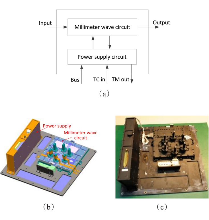
Q band SSPA is mainly used in the high throughput satellite(HTS)Q/V bands transponder,to amplify the broad bandwidth signal to required output power range with good linearity performance. As the complete product,the SSPA is constructed by two parts:millimeter wave circuit and power supply circuit. Millimeter wave circuit is mainly used to realize the millimeter wave signal amplifying,controlling,temperature compensation and power/temperature telemetry(TM). Power supply circuit including DC/DC converter is mainly used for bus voltage transfer,response to the tele-command(TC)data and TM data return,as shown in
As separated into two parts in function,the structure of the SSPA has also two corresponding parts:millimeter wave circuit which is horizontal assembled,and power supply circuit which is vertical installed,with cable connected between them for voltage supply and TM data back. And in this paper,we will mainly focus on the millimeter wave part,and the power supply part will be briefly introduced.
The prototype of millimeter wave circuit is shown in
![]()
Figure 1.Q band SSPA: (a) function diagram, (b) 3-D model of Q band SSPA, (c) photograph of material object
![]()
Figure 2.The prototype and corresponding gain and power distribution of Q band SSPA millimeter wave circuit: (a) prototype, (b) the gain and power distributions of every stage
In Q band SSPA,Multi-way power divider and combiner need to be carefully designed and fabricated to meet the stringent requirements of power combination efficiency at the high frequency,broad bandwidth,and large power condition. The waveguide 1 to 4 power divider and 4 to 1 power combiner are integrated in the millimeter wave circuit structure with the MMICs,bias/filter circuits and controlling printed circuit board(PCB),which realizes the active and passive integration to save dimension and weight,and enhance the efficiency and power at the same time as compact arrangement. The broadband high-power splitter/combiner are designed in two stages of magic T architecture,as shown in
![]()
Figure 3.Q band broadband power divider/combiner (4 ways)
Because of low efficiency and high output power,the huge heat consumption and high thermal flux turned out to be a technical bottleneck for space usage. Especially for this product,the 4 ways power amplifier is integrated in a compact architecture,which further exacerbates the challenge of heat handling. The copper diamond heat sink is used under the GaN MMICs as heat sink for the first stage heat dissipation,which offers nearly 2.8 times thermal conductivity(550 W/C·K)compared to the CuW material(192 W/C·K),with similar coefficient of thermal expansion of GaAs or GaN MMICs. Heat pipes are embedded in the SSPA structure as well to decrease thermal resistance and flux from the heat sink to the housing board. The thermal simulation and infrared thermography measurement show that the GaN MMIC’s shell temperature(from heat sink surface)can be hold under 92.4 oC,which will ensure that the GaN MMICs’ gate temperature controlled lower than 150 oC,to satisfy the space long-life usage requirement,as depicted in
![]()
Figure 4.Q band SSPA thermal simulation and infrared thermography: (a) shell temperature of the GaN MMICs, (b) heat flux at bottom
Q band SSPA millimeter wave circuit is shown in
![]()
Figure 5.Q band SSPA millimeter wave circuit structure: (a) integrated structure, (b) explosion figure
The power supply mainly provides the DC feeding for solid state power amplifier. The +100 V Bus voltage is converted to +20 V by Phase-Shift-Full-Bridge(PSFB)topology,which improves efficiency by using synchronous rectifier technology. Then +20 V output voltage is converted to +5 V and -5 V out voltages by Half-Bridge(HB)topology. +20 V provide drain current to the GaN power amplifier chips,+5 V provide drain current to the gain amplifying and pre-drive stage amplifier chips,-5 V is utilized for the gate bias voltage of all MMICs and temperature compensation circuits.
As
![]()
Figure 6.DC/DC power supply for Q band SSPA (a) topology diagram, (b) output voltage serious simulation results, (c) efficiency vs. 20 V’s current (main power consumption part)
The photograph of the proposed SSPA is shown in
![]()
Figure 7.Q band SSPA measurement results (a) output power and gain vs. frequency, (b) efficiency at rated input power vs. frequency, (c) gain and output power vs. input power, (d) efficiency vs. input power
2 V Band SSPA
V band SSPA is developed for Q/V uplink or inter-sat link. Limited by lower output power of MMICs compared to Q band,8 ways radial-line power combiner/divider is designed for highly integration and compact dimensions,as depicted in
![]()
Figure 8.V band 1 to 8/8 to 1 divider/combiner simulation model and results (a) simulation model, transition and reflections simulation results, (b) transition coefficient, (c) reflection of divide ports, (d) isolation between divide ports
The end stage of V band SSPA is shown in
![]()
Figure 9.End stage of V band SSPA (a) design structure (model and explosive), (b) fabricated V band end stage SSPA (Input side; GaN MMICs units and output side)
The fabricated end stage of V band SSPA is shown in
![]()
Figure 10.V band SSPA product and measured results (a) photograph, (b) measurement results
3 W Band SSPA
W band SSPA is the key unit of W band high throughput communication and microwave remote sensing system. To achieve more than 2 watts output power in the 4 GHz bandwidth,the SSPA used 2 ways combination of high power GaN MMICs. The W band product is also constructed by two parts as Q band SSPA:millimeter wave circuit and power supply circuit,which are connected with cable as well,and placed on one plate.
![]()
Figure 11.W band SSPA millimeter wave circuit (a) millimeter wave circuit schematic, (b) integration structure and explosion figure
PCBs are utilized for DC filter,DC supply,negative voltage transfer,and temperature telemetry. Transition from waveguide and microstrip line are also used. With 0.127 mm thickness quartz substrate,transition loss is extremely reduced to small than 0.15 dB during in the operation frequency range.
![]()
Figure 12.W band magic T model and simulation result (a) model and transmission coefficient, (b) reflection and isolation coefficient
All the units are design and assembled in three-layer structure,for DC supply,microwave channel and magic T load separately,as shown in
The power supply is designed based on two-transistor forward topology. Because the topology can achieve magnetic reset by itself,it is widely utilized for medium and small power range of aerospace power supply. The block diagram is shown in
![]()
Figure 13.Power supplier circuit schematic and efficiency curve (a) schematic, (b) output voltage serious, (c) efficiency vs. 15 V’s current (main power consumption part)
The power supply circuit also includes under voltage protection,over current protection and no negative voltage protection functions. The output voltage telemetry and current telemetry are also provided by the power supply.
The proposed W band SSPA is fabricated and tested for verification. The photograph of the integrated SSPA is shown in
![]()
Figure 14.W band SSPA photograph and measurement results (a) photograph, (b) measurement results
4 Conclusion
Three SSPAs of EHF bands for space payload usage or terminal transmitter are discussed in the paper,including Q band 20 watts,V band 10 watts and W band 2 watts. All the products utilize appropriate waveguide power divider / combiner and GaN HEMT MMICs for high output power achievement. All the millimeter wave parts are highly integrated for demission miniaturization. The contrasts of the proposed SSPAs to the latest reports or literatures of EHF SSPA are summarized in
![]()
Figure 15.V band SSPA and W band SSPA of references (a) V band SSPA of Ref. [
| [ | 33.5~38 GHz | 8~21 W | 14~16 dB | 8%~21% (Millimeter wave part) | Model piece |
| [ | 59~63 GHz | 12.8 W (peak) | 34 dB | 16% (Millimeter wave part) | Model piece |
| [ | 80~100 GHz | 29~33 dBm | 8~12 dBm | / | MMIC |
| [ | 94~98 GHz | 2.5~5 W | 18 dB | 7% (Millimeter wave part) | Model piece |
| This work | 37~42 GHz | 20~30 W | 50 dB | 7%~10% (with power supply) | Space qualified |
| This work | 47~52 GHz | >10 W | >26 dB | 9.5%~11.5% (Millimeter wave part) | Ground transmitter |
| This work | 92~96 GHz | 2~3.5 W | >31 dB | 4.5%~7.1% (with power supply) | Space qualified |
Table 1. Compare with latest literatures
References
[1] Cianca ERNESTINA, Rossi TOMMASO, Yahalom ASHER et al. EHF for Satellite Communications: The New Broadband Frontier, 99, 1858-1881.
[2] W.D. Palmer, I. Abdomerovic, P.M. Asbeck et al. Advancing Silicon mm-wave Transmitter ICs for Satellite Communications, 49-52.
[3] J. P. Fraysse, J. Richard, M. Maignan et al. A 20W Ka-band Radial Solid-State Power Amplifier with 20% Associated Power-Added Efficiency, 688-691(2013).
[4] Datta KUNAL, Roderick JONATHAN, Hashemi HOSSEIN. A 22.4 dBm Two-Way Wilkinson Power-Combined Q-Band SiGe Class-E Power Amplifier With 23% Peak PAE, 1-4(2012).
[5] Peng HUANG, Kaizhe GUO, Yi-Ming YU et al. A 21.08 dBm Q-Band Power Amplifier in 90-nm CMOS Process, 1-4(2014).
[6] KIM-Lien Ngo-Wah, Goel JITENDRA, Yeong-Chang CHOU et al. A V-band Eight-Way Combined Solid-State Power Amplifier With 12.8 Watts Output Power, 1371-1374.
[7] Jian LIU, Wen-Hua CHEN, Zheng-He FENG. Design of a V-Band Power Amplifier/Combiner based on Spatial Power-combining Technique, 1127-1129(2013).
[8] Hamidian AMIN, Portela HENRIQUE, Boeck GEORG. High Power V-Band Power Amplifier, 783-786(2009).
[9] Schellenberg JAMES, Kim BUMJIN, Phan TRONG. W-Band, Broadband 2W GaN MMIC, 1-4.
[10] Ming WANG, Xiao-Qiang XIE, Xiang ZHAO et al. A Compact Four-Way Power Combiner/Divider in W-Band, 47-50(2013).
[11] W. Shaobing, G. Jianfeng, W. Weibo, Z. Junyun. W-band MMIC PA with Ultrahigh Power Density in 100-nm AlGaN/GaN Technology.
[12] Zhang-Ju HOU, Yang YANG, Leung CHIU et al. A W-Band Balanced Power Amplifier Using Broadside Coupled Strip-Line Coupler in SiGe BiCMOS 0.13-μm Technology. IEEE Trans. Circuit and Systems, 65, 2139-2150(2018).
[13] Huei WANG, Samoska LORENE, Gaier TODD et al. Power-Amplifier Modules Covering 70–113 GHz Using MMICs. IEEE Trans. Microw. Theory Tech, 49, 9-16(2019).
[14] Marti DIEGO, Lugani LORENZO, JEAN-François Carlin et al. W-Band MMIC Amplifiers Based on AlInN/GaN HEMTs Grown on Silicon. IEEE Electron Device Lett, 37, 1025-1028(2016).
[15] D. Marti, S. Tirelli, V. Teppati et al. 94-GHz Large-signal Operation of AlInN/GaN High-electron-mobility Transistors on Silicon with Regrown Ohmic Contacts. IEEE Electron Device Lett, 36, 17-19(2015).
[16] Lin H.-C., Rebeiz G. M.. A 110–134-GHz SiGe Amplifier with Peak Output Power of 100-120 mW. IEEE Trans. Microw. Theory Techn, 62, 2990-3000(2014).
[17] Lin H.-C., Rebeiz G. M.. A 70–80-GHz SiGe Amplifier with Peak Output Power of 27.3 dBm. IEEE Trans. Microw. Theory Techn, 64, 2039-2049(2016).
[18] ROBERT R. Ferber, TODD C.Gaier, JOHN C. Pearson et al. W Band Power Amplifier Development for the Herschel HIFI Instrument. Millimeter and Submillimeter Detectors for Astronomy, ISBN: 0-8194-4634-3.2/2003, 468-479.
[19] Schellenberg JAMES, Watkins EDWARD, Micovic MIROSLAV et al. W-Band 5W Solid-State Power Amplifier/Combiner, 240-243.
[20] Dan ZHONG, Jun XU, Mao-Yan WANG et al. A 92–96 GHz W-band Power Amplifier, 187-189(2012).


Set citation alerts for the article
Please enter your email address

© Copyright 2018-2021 | Chinese Laser Press. All Rights Reserved 沪ICP备15018463号-20