
Xie Jing, Li Xiaojuan, Zhang Yan, Li Xiangyang. Design of ultra-low-power readout circuit for 1 024×1 024 UV AlGaN focal plane arrays[J]. Infrared and Laser Engineering, 2020, 49(5): 20190491
- Infrared and Laser Engineering
- Vol. 49, Issue 5, 20190491 (2020)
Abstract
0 Introduction
Recent technological advances, the photoelectric detectors based on GaN with unique optical, electrical and structural properties have gradually matured. Because of their wide tunable direct bandgap, good carrier transport properties, high breakdown fields chemical stability and high robustness, AlGaN based solar-blind UV detector have been studied extensively in ultraviolet (UV) photodetectors. And UV imaging systems have been widely used in defense, scientific research, missile warning, offshore oil monitoring, spectroscopy, chemical and biological threat detection, environmental monitoring, astronomy and so on[
Readout Integrated Circuit (ROIC) is one of the most important parts of UVFPA. And due to the amount of pixels increasing rapidly for large formats resulting in the power consumption of readout circuit increases speedy, the realization of low power consumption has become one of the key challenges for ROIC design. To realize low power, the dynamic windowing and transposition methods have been proposed with the columns outside the window and the unused buffers are powered down[
1 Circuit description
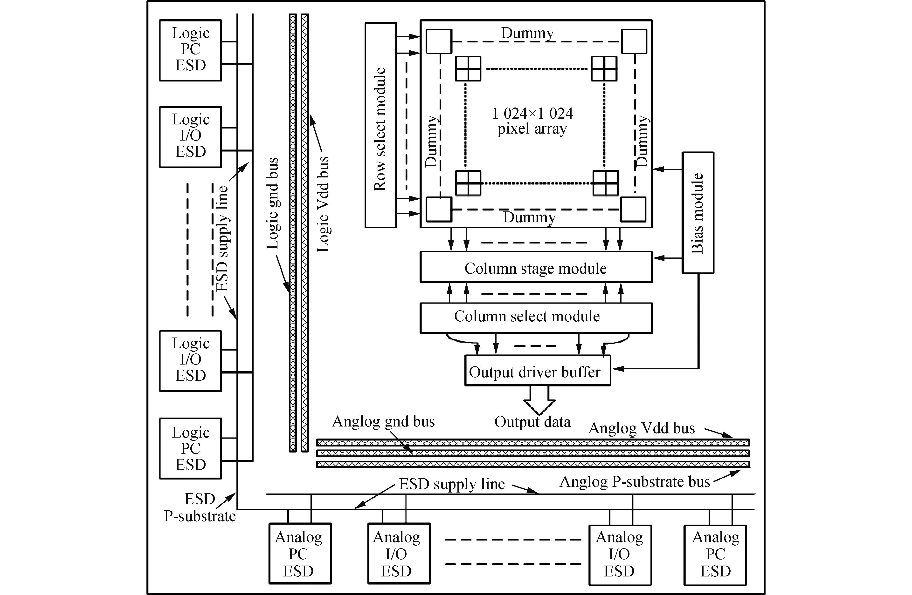
The system architecture of the ROIC with snapshot integration mode is shown in
![]()
Figure 1.System architecture for UV AlGaN FPA readout circuit with whole chip ESD protection
Meanwhile, the whole chip ESD protection network mentioned in this paper are separated into logic and analog ESD protection modules. They are placed at the left and bottom part of the chip separately. The analog and Logic ESD modules are supplied by analog and digital supply lines, respectively, to decrease crosstalk effect. And various methods are adopted to improve robustness of the chip such as multi power clamps, dummy devices and top metal as light barrier covered the whole chip, etc.
This designed readout circuit has adjustable integration time, gain of CTIA and internal bias supplies, and has multi outputs. In addition, this circuit features snapshot mode with integrate-while-read (IWR) and integrate-then-read (ITR) operation that all pixels integrate simultaneously per integration period.
2 Low power implementation
Though direct injection (DI), source-follower per detector (SFD) structures in pixels widely used to decrease power consumption, but they can’t provide constant bias voltage for photodiode resulting in lower conversion factor. Therefore, the CTIA is adopted with stable bias voltage, good linearity, high injection efficiency and wide detecting range. What’s more, to realize larger format FPA of low power, the design of ultra-low-power pixel is the key point, so a single-terminal amplifier using the cascode configuration instead of two- terminal amplifier as pixel amplifier in this paper to optimize the power consumption as small as possible. What’s more, it substantially reduces the power consumption by operating amplifier transistors under subthreshold region and the smallest operational current of CTIA in pixel unit is only 8.5 nA. The current can be expressed as:
The parameter η is subthreshold swing coefficient, and is calculated to between 1 and 3. The process parameters of oxide capacitance per unit area Cox, surface depletion-layer capacitance Csi and interface-trapped capacitance CSS. The parameter k is Boltzmann's constant, T is the absolute temperature in degrees Kelvin, and q is the absolute value of electron charge. In addition, transistor has a linear relationship between the transconductance and the drain current in subthreshold region. Thus, the transconductance to drain current ratio is maximized according to Eq. (5).
![]()
Figure 2.Pixel arrays and column level circuits
The column stage circuits include level shift, column S/H and column buffer circuit. The SF buffer in pixel unit shares a common current source load with other 1 023 pixel cells in the same column, and the pixel signal is transferred through SF buffer. Afterwards, the same current source is also used for level shift circuit, which compensates the voltage drop caused by SF buffer, to save lots of consumption, and thus becomes the second way to reduce power consumption. Compared to pixel S/H circuit which isolates outputs among pixels and get more flexible readout mode, the column S/H and column buffer circuits separate the column output from all pixel outputs to achieve low noise performance.
The third method to decrease power dissipation is the novel design of column buffer, which is shown in
![]()
Figure 3.Design of column buffer circuit
Generally, these methods were introduced in UVFPA readout circuit to realize low power consumption for large format arrays. Meanwhile the ROIC also supports bias current adjustments to optimize power dissipation for better performances. The ROIC has a 3-bit digital-to-analog converter (DAC) on chip which generates adjustable bias-current for allover chip.
![]()
Figure 4.Architecture of whole chip bias supply
The total power consumption can be calculated in Eq. (2).
Where Ppixel is the power of per pixel; Pcolumn is the power of output-stage; Pbias is the power of current bias circuit; Plogic is the power of digital control circuit which can be ignored; Pcolumn refers to power of one column-stage circuit which contains SF power Psf; level-shift power Pls and column buffer Pcb. M is column and N is row that both of them are equal to 1 024 in this ROIC. There are totally 8 output buffers in this design and every 128 column shares an output buffer, so n equals 8 in this equation. As mentioned in this equation we can see that the most part of power dissipation comes from pixel arrays and the lower power of the pixel, the lower power of the whole chip.
The novel design of common current source load for SF buffer in pixels and level shift circuits is used to decrease power consumption for this ROIC, the total power consumption can be changed to calculated in Eq. (8). Compared to Eq.(7), the power of Psf reduced significantly.
| Parameter | Previous[ | This paper |
| Array format | 128×128 | 1 024×1 024 |
| Pixel current/nA | 499 | 8.5 |
| Total power consumption/mW | 49.2 | 67.3 |
Table 1. Comparision of power consumption
Compared to that, the pixel current reduces from 499 nA to 8.5 nA after optimizing design, which improved the power consumption for large pixel arrays application. What is more, the total consumption is also reduced greatly in
3 Experimental results
The UVFPA readout circuit is designed and fabricated in SMIC 0.18 µm 1P6M mixed signal process with 3.3 V supply.
![]()
Figure 5.Die photograph of ROIC chip
![]()
Figure 6.Test platform of the ROIC chip and test result
The measurement results of 1 024×1 024 ROIC with eight outputs by acquisition card NI6366 are shown in
![]()
Figure 7.Measurement results of 1 024×1 024 ROIC with eight outputs by acquisition card
The performances include operate mode, output swing range, integration capacitor charge capacity and power supply, etc. The summarized specifications of the 1 024×1 024 readout circuit are detailed in
| Parameter | Measurement |
| Array format | 1 024×1 024 |
| Pixel size | 18 µm×18 µm |
| Operate mode | Snapshot |
| Pixel current/nA | 8.5 |
| Power consumption | 67.3 mW @2 MHz |
| Frame rate | 15 Hz(limited by speed of acquisition card) |
| Integration capacitor Charge capacity | 0.11 M |
| Output swing/V | 1.8 |
| Power supply/V | 3.3 |
| Chip area | 19.30 mm×20.17 mm |
Table 2. ROIC of UVFPA specifications
4 Conclusion
In this paper, these methods are adopted to optimize power consumption for UVFPA readout circuit, which are single-terminal amplifier with static current 8.5 nA as CTIA amplifier, common current source load for SF buffer in column pixels and level shift circuits, and time-sharing tail current source for column buffer. As well as, the UVFPA ROIC has a format of 1 024×1 024 and pixel pitch of 18 µm with 10 fF and 110 fF selectable integration capacitors with a variable integration time. Meanwhile, the ROIC operates in snapshot integration mode which has Integrate-Then-Read (ITR) and Integrate-While-Read (IWR) read modes respectively. Above all, the ROIC accomplished an ultra-lower power consumption of 67.3 mW at 2 MHz all frame rate in a 1 024×1 024 FPA with 3.3 V supply voltage. What’s more, it has been fabricated in SMIC 0.18 µm 1P6M mixed signal process and achieved better performances.
References
[1] Kung P, Yasan A, McClintock R, et al. Future of AlxGa1xN materials device technology f ultraviolet photodetects[C]SPIE, 2002, 4650: 199206.
[2] Li Xiangyang, Xu Jintong, Zhang Yan, et al. AlGaNbased material acterizations recent development of related solarblind ultraviolet detects[C]SPIE, 2009, 7518(751802): 18.
[4] Ryan McClintock, Manijeh Razeghi. Solarblind photodetects focal plane arrays based on AlGaN2012[C]SPIE, 2015, 9555:955502.
[5] Zhou Juanjuan, Zhang Yacong, Lu Wengao, et al. A low power readout circuit f 640 × 512 IRFPA with dynamic windowing readout[C]IEEE International Conference on Electron Devices & Solidstate Circuit. 2014,
[6] Zhao Hongliang, Zhao Yiqiang, Song Yiwei , et al. A low power cryogenic CMOS ROIC f 512×512 infrared focal plane array[C]IEEE International Conference of Electron Devices SolidState Circuits, 2011: 12.
[9] Fossum E R, Pain B. Infrared readout electronics f space science senss:state of the art future directions[C]SPIE, 1993, 2020: 262282.
[10] Xie Jing, Wang Ling, Wang Jiqiang, et al. ESD design of radiationhardened f UV AlGaN focal plane arrays readout circuit[C]SPIE, 2018, 10846:108461M.
[11] Shuping Li, Kai Fu, Yan Wang. Design method of readout circuit for large format array IRFPA. Chinese Journal of Electron Devices, 41, 1507-1511(2018).


Set citation alerts for the article
Please enter your email address

© Copyright 2018-2021 | Chinese Laser Press. All Rights Reserved 沪ICP备15018463号-20