
Xiao SHAO, Rui-Heng LIU, Liang WANG, Jing CHU, Guang-Hui BAI, Sheng-Qiang BAI, Ming GU, Li-Na ZHANG, Wei MA, Li-Dong CHEN. Interfacial Stress Analysis on Skutterudite-based Thermoelectric Joints under Service Conditions [J]. Journal of Inorganic Materials, 2020, 35(2): 224
- Journal of Inorganic Materials
- Vol. 35, Issue 2, 224 (2020)
Abstract
Thermoelectric (TE) technology has attracted great attention because it can convert heat into electric power directly with the advantages of no moving parts and long durability, especially for the applications in deep space exploration, waste heat recovery, and other special fields[
As the SKD device steps forward to industrial application from laboratory[
Numerical analysis for residual interfacial stress in multilayer system was well studied in the past decades. It was recognized that the coefficient of thermal expansion (CTE) of the component layers plays a critical role on interfacial reliability[
This study reports a numerical analysis model based on finite element simulation method to investigate the dynamic interfacial stress at the SKD/DBL joint by taking the microstructure evolution into account. A single- layer model was established, and the interfacial stress in the TE joints with different DBL was calculated. Based on the experimental results on the interface observation and properties measuring of reaction layers, a multilayer model considering microstructure evolution was built to quantitively simulate the stress state of the aged TE joints. The tensile test results of SKD/Nb joints matched well with the simulation results.
1 Finite element model and experi-mental procedure
1.1 Governing equation of thermal-structural model
A transient thermal-structural model is applied for stress in SKD/DBL joints to simulate the sintering- cooling process. Residual stress results from change of temperature and difference of material properties. For cooling period, the transient thermal conducting equation can be derived according to energy conservation law:
Where T is absolute temperature, ρ is the density, Cp is isobaric heat capacity, q is the heat flux vector, $\dot{q}$ is heat generation rate, [κ] stands for thermal conductivity matrix dependent with T. From Eq. (1-2), the temperature distribution in model can be worked out.
Once temperature decreases, the difference between CTE of SKD and Nb causes displacement, which can be converted to strain, and then results in stress according to generalized Hooke’s law. Thus the thermal-structural governing equation can be expressed as[
Where σ and ε are stress and strain vectors respectively, [D] is stiffness matrix, α is CTE vector, ΔT is the difference between present temperature and reference temperature (T0). Finally, the stress distribution can be figured out.
For a certain site in materials, stress tensor can be divided to three principle stresses: σ1, σ2, σ3, from large to small, respectively. According to the first strength theory, the maximum principle stress is the main reason for fracture, which coincides well with the fracture of brittle materials’ uniaxial tension. Therefore, the first principle stress σ1 is chosen to evaluate stress intensity.
In initial state (t=0), adjacent materials are already bonded closely to form a zero-stress state. Thus, the initial temperature (960 K) is reference temperature (T0) of thermal expansion. Then in cooling process, joint’s diameter is assumed to be unchanged, meanwhile upper and lower end could move vertically. Besides, model’s round side is considered as thermal insulated. On the end side surfaces, effect of cooling is also simplified as natural convection in air, in which the heat transfer coefficient was set to be 10 W·m2·K-1.
1.2 Experimental procedures
SKD/Nb joints were fabricated and aged for tensile test. Yb0.3Co4Sb12 (SKD) powders and Nb foil ((0.025± 0.015) mm) were loaded into a graphite die with a diameter of 50 mm, and then sintered by hot pressed for 90 min at 690 ℃ and 60 MPa under Ar atmosphere. Nb foil was placed between two SKD layers to form a sandwich structure. The obtained joint (ϕ50 mm×4 mm) was then cut into small cylinders (ϕ10 mm) and sealed in quartz ampules under vacuum. The sealed ampules were aged under 600 and 650 ℃ in furnace for various time, and the aged joints were denoted as “temperature-aging time”, such as 600-10 d. The tensile strength was measured by Instron-5566 universal testing system at room temperature. The microstructures of interface and fracture surface were observed by SEM (ZEISS Spura 55). The constituents of interface were measured by EDS (Oxford Instrument).
2 Results and discussion
2.1 Influence of materials properties in single- layer model
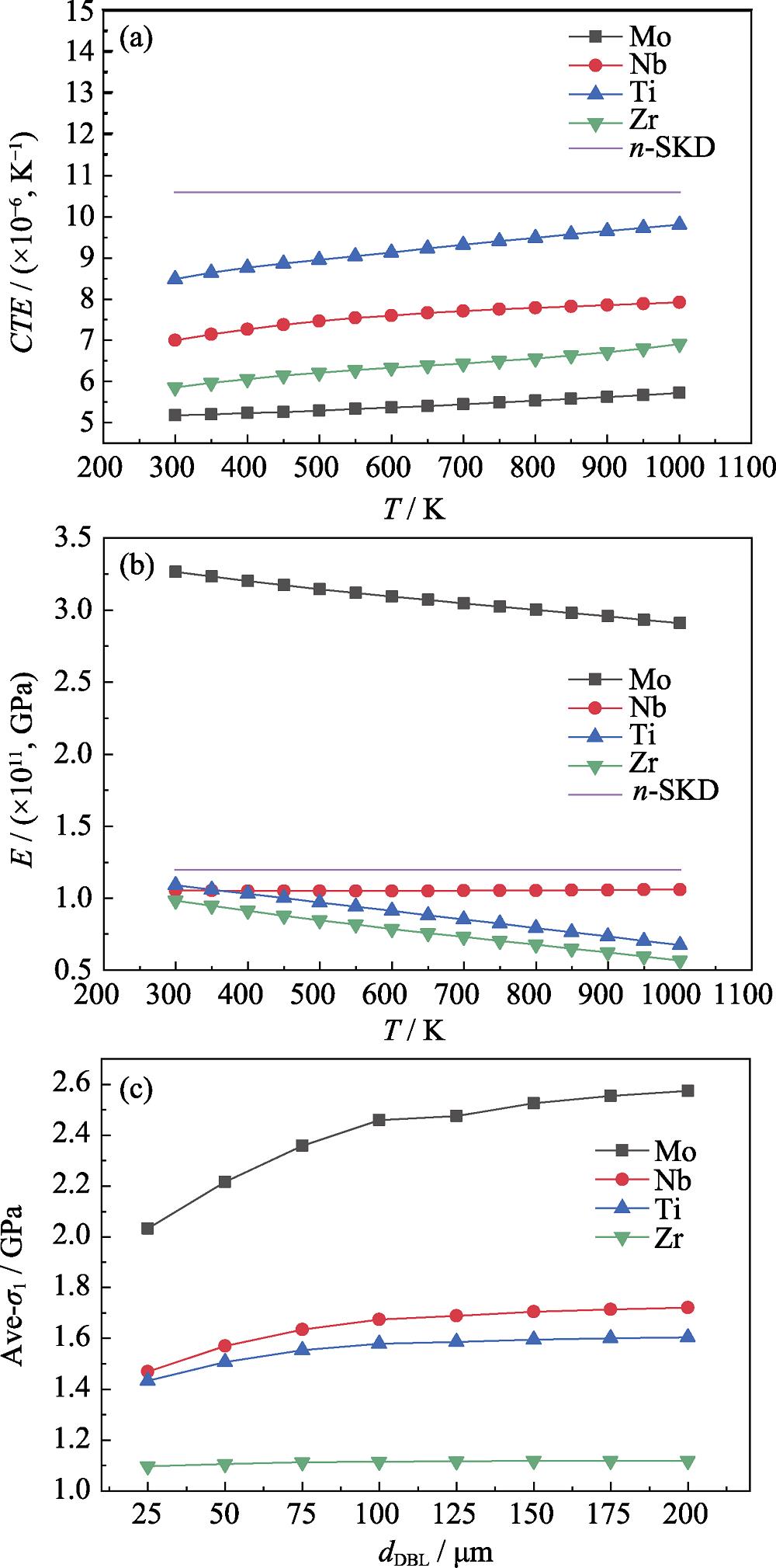
Nb, Mo, Zr, Ti were chosen as the DBL candidates for SKD[
![]()
Figure .(a)
2.2 Influence of thickness of layers in multilayer model
Actually, all the SKD joints undergo the elemental diffusion and chemical reaction during long-time service at high temperature[
![]()
Figure .
Thus, multilayer model was built to find out the influence of micropores and diffusion layers.
To simplify the modeling and calculation, there’re some requisite assumptions in the model: (1) CoSb2 and NbSb2 layers are assumed to be totally flat; (2) Micropores are of ellipsoid shape, in which x and y semi-major axis (a and b) are equal to a multiple of z semi-major axis (c); (3) Micropores locate on the interface between NbSb2 and CoSb2 periodically; (4) Diameter of cylindrical model is reduced; (5) Materials are seen as isotropic and completely linear-elastic; (6) Part of material properties (Table A1) is treated as constant value or simple function of temperature because of lack in experimental data. Combining materials’ molar mass and density listed in Table A1, relationships of thickness of each layer can be obtained, as shown in Table 1. Thus, total volume of micropores ought to equal the volume difference between models before and after aging. Therefore, the relationship (Eq. (5)) between average micropore size and thickness of NbSb2 is listed:
| Material | SKD | CoSb2 | NbSb2[ | ZrSb2[ | Nb | Zr |
|---|---|---|---|---|---|---|
| Molar Mass/(g·mol-1) | 424.21 | 302.45 | 336.43 | 334.82 | 92.91 | 91.22 |
| Density/(g·cm-3) | 7.80* | 8.36 | 8.29 | 7.62 | 8.57-8.45 | 6.5-6.4 |
| Young’s modulus/GPa | 120* | 160 | 186.1 | 135.7 | 104.8-105.7 | 97-57 |
| Poisson’s ratio | 0.21[ | 0.23 | 0.21 | 0.243 | 0.382-0.394 | 0.34 |
| Thermal conductivity/(W·m-1·K-1) | 3.04-4.05* | 6.8-12.5[ | 24 | 10 | 55-65 | 20-25 |
| Thermal expansion/(×10-6, K-1) | 10-11[ | 14-23[ | 8.4 | 9.7 | 7-7.8 | 5.9-6.9 |
| Heat capacity/(J·g-1·K-1) | 0.22-0.23* | 0.247 | 0.222 | 0.223 | 0.27-0.45 | 0.28-0.34 |
Table 1.
Basic properties including molar mass, density, Young’s modulus, Poisson’s ratio, thermal conductivity, thermal expansions and heat capacity for series of materials
Where r is radius of model, dNbSb2 is thickness of NbSb2, ΔV is total volume of micropores, m is the ratio of a (or b) to c, n is number of micropores at given total micropore volume. As long as micropores’ shape, numbers and positions are certain, dNbSb2 is expected to decide the extent of aging. Micropores’ positions are considered to uniformly distribute at the CoSb2/NbSb2 interface. The number of micropores n was set as 1, 3, 7, and the distributions for each number are shown in Fig. 2(b-d). According to calculation results presented in Fig. A3, the ratio of a (or b) to c (m) made little difference to stress distribution, which won’t be discussed in the next part.
The diffusion and reaction process of SKD/Zr joint is similar with SKD/Nb, and the reaction layer is ZrSb2[
The evolution of the interface can be simplified descripted by 3 parameters of n, dDBL and dNbSb2. The positions of micropores need to be set manually for each different n. When n changes from 1 to 7, the micropore size decreases from 5.3 μm to 1.2 μm. Furthermore, to eliminate the influence of abnormal stress caused by low-quality elements mesh in much thinner barrier layer and diffusion layer, average first principle stress is applied to evaluate interfacial stress intensity. Fig. 2(a) gives the initial stress distribution of SKD/Nb interface which is the same with the single layer model. The stress concentrates on Nb layer, and the maximum principle stresses of Nb/SKD interface is 2.383 and 1.46 GPa, respectively. Fig. 2(b-d) shows the σ1 distribution in multilayer model with different micropore numbers n at the same given ΔV. After aging, all stress values with increasing n are much higher than the initial ones. For all cases, maximum stresses are found at the CoSb2 layers. When dNbSb2=10 μm, the maximum σ1 are 5.83 GPa for n=1 and 7.79 GPa for n=7, indicating that the diffusion reaction induce large internal stress. Fig. 3 shows the dDBL and dNbSb2 dependent σ1 at SKD/CoSb2 and CoSb2/NbSb2 interfaces. The average stress of CoSb2/NbSb2 interface is always the largest value for different n, indicating that CoSb2/NbSb2 is the most unstable interface. In Fig. 3(b, e, h), contour lines are approximately parallel to dDBL axis, which means the thickness of reactive NbSb2 plays a dominate role on stress of CoSb2/NbSb2 interface.
![]()
Figure .Variations of average
2.3 Tensile test results and validation of models
SKD/Nb joints are fabricated and aged for tensile test. After fracture, bonding strength are calculated by Eq. (6):
Where σt is tensile strength, Fmax is the maximum load, A is base area of joints. The results are listed in Table 2. It is obvious that accelerated aging worsens interfacial bonding severely. With the dNbSb2 grows from 0 to 12 μm, the tensile strength decreases from 9.68 MPa to 1.46 MPa. The decreasing trend of tensile strength is consistent with the increasing trend of calculated stress. Furthermore, after tension, by comparing structures and compositions of the fracture surfaces, location of the weakest interface can be found. All of the aged joints break at CoSb2 layer (Fig. 4(d-e)), while the unaged joints break at SKD/Nb interface (Fig. 4(a)). With elevated aging temperature or prolonged aging time, the proportions of CoSb2 on fracture surface (SKD side, Fig. 4(d)) increases obviously (Table 2), indicating that the fracture locations tend to be the CoSb2/NbSb2 interface. The fracture locations are completely consistent with calculation results. All of the experimental results verify the validity of above simulation model.
| Joints | Ave- | Fracture position | Fracture composition | ||||
|---|---|---|---|---|---|---|---|
| 0 d | 0 | 0 | 0 | 1.46 | (9.68±1.70) | Nb/ SKD | (Nb+ NbSb2)/(3%CoSb2+97% SKD) |
| 600-5 d | 2 | 2.02 | 3 | 2.72 | (4.63±2.12) | CoSb2/NbSb2 | NbSb2/(36%CoSb2+64% SKD) |
| 600-10 d | 3 | 2.21 | 3 | 2.80 | (3.39±1.44) | CoSb2/NbSb2 | NbSb2/(47%CoSb2+53% SKD) |
| 650-5 d | 7 | 4.13 | 1 | 3.07 | (4.44±1.50) | CoSb2/NbSb2 | NbSb2/(80%CoSb2+20% SKD) |
| 650-10 d | 12 | 5.20 | 1 | 3.42 | (1.46±0.38) | CoSb2/NbSb2 | NbSb2/(97%CoSb2+3% SKD) |
Table 2.
Thicknesses of NbSb2 layer dNbSb2, average sizes of micropores c, tensile strengths σt, maximum calculated stresses Ave-σ1 and the location interfaces, compositions of tensile fracture surface for series of aging SKD/Nb joints。。
![]()
Figure .EDS mappings of (a, d) interfaces and (b, e) fracture surfaces of (a-b) unaged joint and (d-e) sample 650-10d (White line indicating the fracture surface, and white arrow indicating direction of observation in (b) or (d)); Total element data were shown in table (c) for figure (b) and in table (f) for figure (e)
4 Conclusion
In this study, a single-layer model was established to calculate the interfacial stress in the TE joints with different DBL. It’s found that the DBL materials with small modulus and similar CTE with SKD can reduce the interfacial stress. Based on the experimental results, a multilayer model considering microstructure evolution is built to quantitively simulate the stress state of the aged TE joints. Large thickness of reaction layers and volume changes can intensify stress at interface remarkably. Both in SKD/Zr and SKD/Nb joints, the biggest first principle stress locates at CoSb2 layer. Tensile test results of SKD/ Nb joints fit simulation results well, proving the feasibility of this model to simulate the stress state in multilayer system containing complex microstructures, which is helpful to design the high stability electrode interface structure for SKD TE devices.
Supporting materials:
Supporting materials related to this article can be found at
![]()
Figure .(a) Finite element model of SKD/Nb joint with pores, detailed meshes of (b) NbSb2 layer and (c) CoSb2 layer
![]()
Figure .Interface structures and line scans of joints
![]()
Figure .Relationships between interface stresses and pores major axis ratios
![]()
Figure .(a) Calculated stress state of SKD/Zr joint with the Zr layer of 25 μm and the micropores number
参考文献:
[1] FAILAMANI F, BROZ P, MACCIÒ D, et al. Constitution of the systems {V,Nb,Ta}-Sb and physical properties of di-antimonides {V,Nb,Ta}Sb2. Intermetallics, 2015, 65: 94-110.
[2] TAVASSOLI A, GRYTSIV A, FAILAMANI F, et al. Constitution of the binary M-Sb systems (M=Ti, Zr, Hf) and physical properties of MSb2. Intermetallics, 2018, 94: 119-132.
[3] SALVADOR J R, YANG J, SHI X, et al. Transport and mechanical properties of Yb-filled skutterudites. Philosophical Magazine, 2009, 89(19): 1517-1534.
[4] GOTO Y, MIYAO S, KAMIHARA Y, et al. Electrical/thermal transport and electronic structure of the binary cobalt pnictides CoPn2 (Pn=As and Sb). AIP Advances, 2015, 5(6): 067147.
[5] ZHAO D, LI X, JIANG W, et al. Fabrication of CoSb3/MoCu thermoelectric joint by one-step SPS and evaluation. Journal of Inorganic Materials, 2009, 24(3): 545-548.
[6] BÖRNSTEIN L. CoSb2: Crystal Structure, Physical Properties, in: Madelung U R O, Schulz M (Ed.), Non-tetrahedrally Bonded Binary Compounds ii. Berlin: Springer-Verlag, 2000.
References
[1] E BELL L. Cooling, heating, generating power and recovering waste heat with thermoelectric systems. Science, 321, 1457-1461(2008).
[2] D CHAMPIER. Thermoelectric generators: a review of applications. Energy Conversion and Management, 140, 167-181(2017).
[3] L CHEN, S BAI, Q ZHANG. Technologies and applications of thermoelectric devices: current status, challenges and prospects. Journal of Inorganic Materials, 34, 279(2019).
[4] C SALES B, D MANDRUS, K WILLIAMS R. Filled skutterudite antimonides: a new class of thermoelectric materials. Science, 272, 1325-1328(1996).
[5] H LIU, X SHI, F XU et al. Copper ion liquid-like thermoelectrics. Nature Materials, 11, 422-425(2012).
[6] D ZHAO L, H LO S, Y ZHANG et al. Ultralow thermal conductivity and high thermoelectric figure of merit in SnSe crystals. Nature, 508, 373-377(2014).
[7] H ZHANG Q, Y HUANG X, Q BAI S et al. Thermoelectric devices for power generation: recent progress and future challenges. Advanced Engineering Materials, 18, 194-213(2016).
[8] R HE, G SCHIERNING, K NIELSCH. Thermoelectric devices: a review of devices, architectures, and contact optimization. Advanced Materials Technologies, 3, 1700256(2018).
[9] Q ZHANG, J LIAO, Y TANG et al. Realizing a thermoelectric conversion efficiency of 12% in bismuth telluride/skutterudite segmented modules through full-parameter optimization and energy- loss minimized integration. Energy Environ. Sci., 10, 956-963(2017).
[10] Z YAO, P QIU, X LI et al. Investigation on quick fabrication of n-type filled skutterudites. Journal of Inorganic Materials, 31, 1375-1382(2016).
[11] V RAVI, S FIRDOSY, T CAILLAT et al. Mechanical properties of thermoelectric skutterudites. AIP Conference Proceedings, 969, 656-662(2008).
[12] R SALVADOR J, J YANG, X SHI et al. Transport and mechanical properties of Yb-filled skutterudites. Philosophical Magazine, 89, 1517-1534(2009).
[13] T DAHAL, S KIM H, S GAHLAWAT et al. Transport and mechanical properties of the double-filled p-type skutterudites La0.68Ce0.22Fe4-
[14] Z RUAN, L LIU, P ZHAI et al. Residual strength degradation of CoSb3 skutterudite compounds under low-cycle fatigue loading. Journal of Electronic Materials, 41, 1487-1492(2012).
[15] P WEN, Y ZHU, J CHEN et al. The microstructure and thermoelectric properties of Yb-filled skutterudite Yb0.1Co4Sb12 under cyclic thermal loading. Journal of Materials Engineering and Performance, 25, 4764-4768(2016).
[16] D ZHAO, X LI, L HE et al. Interfacial evolution behavior and reliability evaluation of CoSb(3)/Ti/Mo-Cu thermoelectric joints during accelerated thermal aging. Journal of Alloys and Compounds, 477, 425-431(2009).
[17] L SHI, X HUANG, M GU et al. Interfacial structure and stability in Ni/SKD/Ti/Ni skutterudite thermoelements. Surface and Coatings Technology, 285, 312-317(2016).
[18] C FAN X, M GU, X SHI et al. Fabrication and reliability evaluation of Yb0.3Co4Sb12/Mo-Ti/Mo-Cu/Ni thermoelectric joints. Ceramics International, 41, 7590-7595(2015).
[19] T WOJCIECHOWSKI K, R ZYBALA, R MANIA. High temperature CoSb3-Cu junctions. Microelectronics Reliability, 51, 1198-1202(2011).
[20] M GU, X XIA, X LI et al. Microstructural evolution of the interfacial layer in the Ti-Al/Yb0.6Co4Sb12 thermoelectric joints at high temperature. Journal of Alloys and Compounds, 610, 665-670(2014).
[21] S TANG Y, Q BAI S, D REN D et al. Interface structure and electrical property of Yb0.3Co4Sb12/Mo-Cu element prepared by welding using Ag-Cu-Zn solder. Journal of Inorganic Materials, 30, 256-260(2015).
[22] M GU, S BAI, J WU et al. A high throughput strategy to screen interfacial diffusion barrier materials for thermoelectric modules. Journal of Materials Research, 34, 1179-1187(2019).
[23] L CHEN, S BAI, R LIU et al. Interface stability of skutterudite thermoelectric materials/Ti88Al12. Journal of Inorganic Materials, 33, 889-894(2018).
[24] S EL-GENK M, H SABER H, T CAILLAT et al. Tests results and performance comparisons of coated and un-coated skutterudite based segmented unicouples. Energy Conversion and Management, 47, 174-200(2006).
[25] H HSUEH C. Thermal stresses in elastic multilayer systems. Thin Solid Films, 418, 182-188(2002).
[26] M HAN, J HUANG, S CHEN. The influence of interface morphology on the stress distribution in double-ceramic-layer thermal barrier coatings. Ceramics International, 41, 4312-4325(2015).
[27] Y LI, Q YANG X, C ZHAI P et al. Thermal stress simulation and optimum design of CoSb3/Bi2Te3 thermoelectric unicouples with graded interlayers. AIP Conference Proceedings, 973, 297-302(2008).
[28] X JIA, Y GAO. Estimation of thermoelectric and mechanical performances of segmented thermoelectric generators under optimal operating conditions. Applied Thermal Engineering, 73, 335-342(2014).
[29] M GU, X XIA, X HUANG et al. Study on the interfacial stability of p-type Ti/Ce


Set citation alerts for the article
Please enter your email address

© Copyright 2018-2021 | Chinese Laser Press. All Rights Reserved 沪ICP备15018463号-20