• Photonics Research
  • Vol. 6, Issue 4, 290 (2018)
Yue Wang1, Bing Wang1, Wardhana A. Sasangka1, Shuyu Bao1、2, Yiping Zhang2, Hilmi Volkan Demir2, Jurgen Michel1、3, Kenneth Eng Kian Lee1, Soon Fatt Yoon1、2, Eugene A. Fitzgerald1、3, Chuan Seng Tan1、2、4, and Kwang Hong Lee1、*
Author Affiliations
  • 1Low Energy Electronic Systems (LEES), Singapore-MIT Alliance for Research and Technology (SMART), 1 CREATE Way, #10-01 CREATE Tower, Singapore 138602, Singapore
  • 2School of Electrical and Electronic Engineering, Nanyang Technological University, 50 Nanyang Avenue, Singapore 639798, Singapore
  • 3Department of Materials Science and Engineering, Massachusetts Institute of Technology, Cambridge, Massachusetts 02139, USA
  • 4e-mail: tancs@ntu.edu.sg
  • show less
    DOI: 10.1364/PRJ.6.000290 Cite this Article Set citation alerts
    Yue Wang, Bing Wang, Wardhana A. Sasangka, Shuyu Bao, Yiping Zhang, Hilmi Volkan Demir, Jurgen Michel, Kenneth Eng Kian Lee, Soon Fatt Yoon, Eugene A. Fitzgerald, Chuan Seng Tan, Kwang Hong Lee. High-performance AlGaInP light-emitting diodes integrated on silicon through a superior quality germanium-on-insulator[J]. Photonics Research, 2018, 6(4): 290 Copy Citation Text show less
    Schematic flow of the fabrication of germanium-on-insulator (GOI) substrates with low threading dislocation density (TDD). All substrates are 200 mm in diameter.
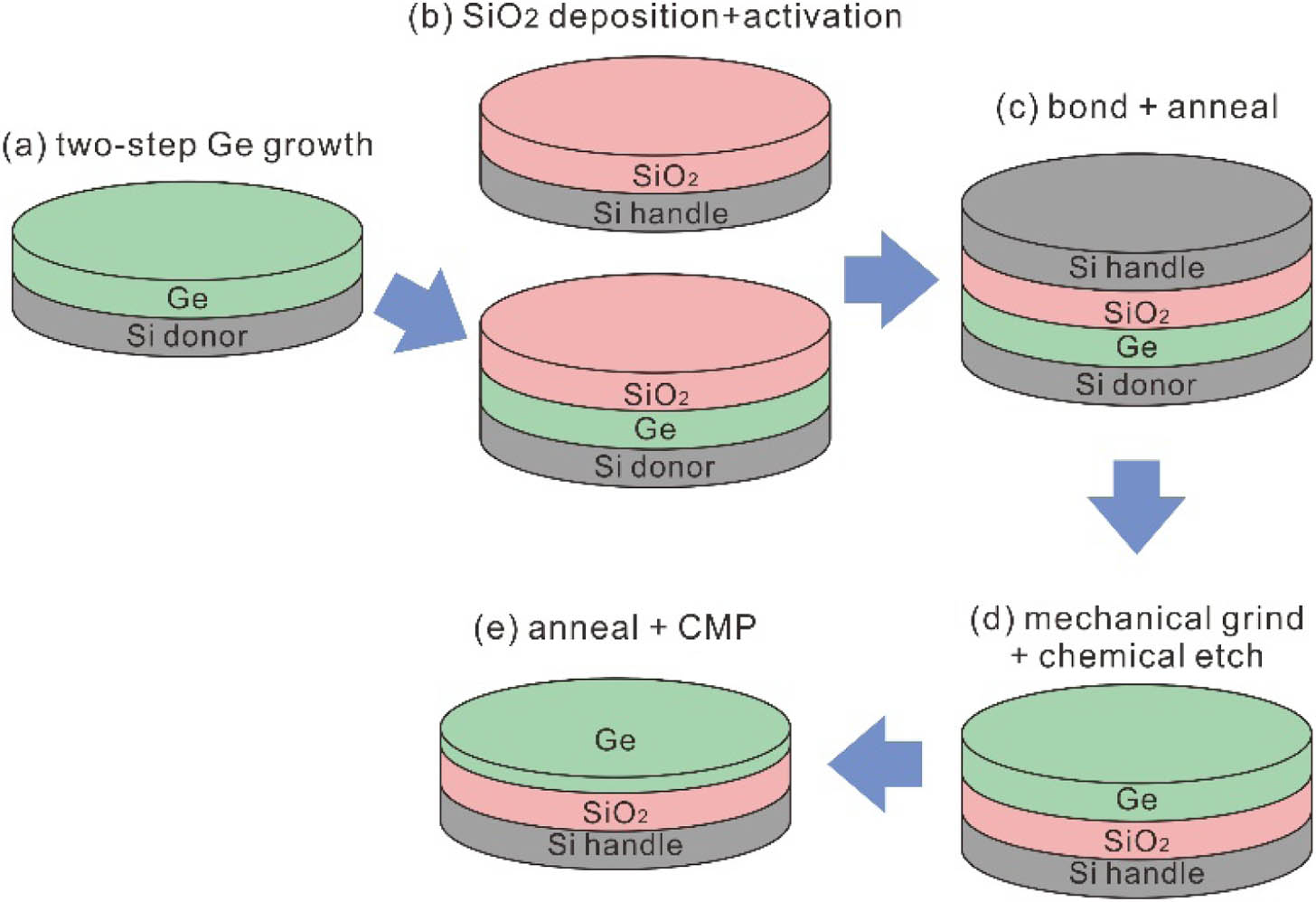
    Fig. 1. Schematic flow of the fabrication of germanium-on-insulator (GOI) substrates with low threading dislocation density (TDD). All substrates are 200 mm in diameter.
    Schematic layout and layer structure of (Al0.3Ga0.7)0.51In0.49P/Ga0.51In0.49P multi-quantum well (MQW) LEDs on a GOI substrate.
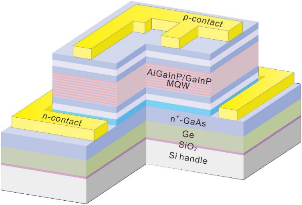
    Fig. 2. Schematic layout and layer structure of (Al0.3Ga0.7)0.51In0.49P/Ga0.51In0.49P multi-quantum well (MQW) LEDs on a GOI substrate.
    Etch pit density (EPD) determination for (a) GOI substrate after layer transfer, (b) GOI substrate after O2 annealing and CMP processes, and (c) commercially available Ge/Si substrate.
    Fig. 3. Etch pit density (EPD) determination for (a) GOI substrate after layer transfer, (b) GOI substrate after O2 annealing and CMP processes, and (c) commercially available Ge/Si substrate.
    Characteristics of the GOI substrate after O2 annealing and CMP processes. (a) Cross-sectional transmission electron microscopy (X-TEM) bright field image of the GOI substrate; inset is a high-resolution TEM image of the Ge layer. (b) HRXRD curves of the commercial Ge/Si and our GOI substrates. The Ge signal curve is symmetric, which suggests that the intermixed Si1−xGex material near the Ge/Si interface was removed after the annealing. (c) A 5 μm×5 μm atomic force microscopic scan of the GOI substrate. The RMS roughness is ∼0.2 nm.
    Fig. 4. Characteristics of the GOI substrate after O2 annealing and CMP processes. (a) Cross-sectional transmission electron microscopy (X-TEM) bright field image of the GOI substrate; inset is a high-resolution TEM image of the Ge layer. (b) HRXRD curves of the commercial Ge/Si and our GOI substrates. The Ge signal curve is symmetric, which suggests that the intermixed Si1xGex material near the Ge/Si interface was removed after the annealing. (c) A 5  μm×5  μm atomic force microscopic scan of the GOI substrate. The RMS roughness is 0.2  nm.
    X-TEM bright field images showing LEDs grown on (a) a commercial Ge/Si substrate and (b) our GOI substrate after it had been subjected to O2 annealing and CMP processes.
    Fig. 5. X-TEM bright field images showing LEDs grown on (a) a commercial Ge/Si substrate and (b) our GOI substrate after it had been subjected to O2 annealing and CMP processes.
    I–V characteristics for LEDs on bulk Ge, our GOI, and commercial Ge/Si substrates, with mesa size of 600 μm×600 μm. The ideality factor for the LEDs on Ge, GOI, and commercial Ge/Si is 1.207, 1.308, and 1.494, respectively.
    Fig. 6. I–V characteristics for LEDs on bulk Ge, our GOI, and commercial Ge/Si substrates, with mesa size of 600  μm×600  μm. The ideality factor for the LEDs on Ge, GOI, and commercial Ge/Si is 1.207, 1.308, and 1.494, respectively.
    (a) Room-temperature photoluminescence (PL) spectra (with input laser power of 20 mW) and (b) electroluminescence (EL) spectra (with injection current of 20 mA) of the LEDs grown on three different substrates.
    Fig. 7. (a) Room-temperature photoluminescence (PL) spectra (with input laser power of 20 mW) and (b) electroluminescence (EL) spectra (with injection current of 20 mA) of the LEDs grown on three different substrates.
    (a) Optical output power (L–I) and external quantum efficiency (EQE) of LEDs grown on commercial Ge/Si and our GOI substrates measured by an integrating sphere that is 1 m in diameter. (b) Optical images of emitting 100 μm×100 μm LEDs on the commercial Ge/Si and our GOI substrates under a continuous injection current of 20 mA.
    Fig. 8. (a) Optical output power (L–I) and external quantum efficiency (EQE) of LEDs grown on commercial Ge/Si and our GOI substrates measured by an integrating sphere that is 1 m in diameter. (b) Optical images of emitting 100  μm×100  μm LEDs on the commercial Ge/Si and our GOI substrates under a continuous injection current of 20 mA.
    Junction temperature versus peak emission wavelength of LEDs grown on different substrates.
    Fig. 9. Junction temperature versus peak emission wavelength of LEDs grown on different substrates.
    Reliability of LEDs on commercial Ge/Si and our GOI substrates under a stressing condition of 200 A/cm2 at room temperature.
    Fig. 10. Reliability of LEDs on commercial Ge/Si and our GOI substrates under a stressing condition of 200  A/cm2 at room temperature.
    Schematics show the integration of (a) Si-CMOS and red LEDs, and (b) red, green, and blue LEDs with Si-CMOS control circuitry through multi-wafer bonding and layer transfer processes.
    Fig. 11. Schematics show the integration of (a) Si-CMOS and red LEDs, and (b) red, green, and blue LEDs with Si-CMOS control circuitry through multi-wafer bonding and layer transfer processes.
     SiGe Graded Buffer [15]Selective Epitaxial Growth (SEG) [16]Two-Step Growth Approach [13]This Work
    Ge thickness (μm)12110.6
    Dislocation density (cm2)2.1×1061×1065×1071×106
    RMS surface roughness (nm)24.2NA (undulated surface)1–20.2 (CMP)
    Table 1. Quality of Ge Epitaxial Films on Si Substrates Using Different Approaches
     Bao et al. [22]Chulukuri et al. [8]Kwon et al. on Ge [7]Kwon et al. on SiGe Graded Buffer [7]This Work
    Number of quantum wells514410
    DBRNoNoYesYesNo
    Output power (mW/mm2)<0.10.001750.3270.5311.3
    Ideality factorNANA1.951.951.308
    Table 2. Performance of Red LEDs on Si Substrates from Literatures
    Yue Wang, Bing Wang, Wardhana A. Sasangka, Shuyu Bao, Yiping Zhang, Hilmi Volkan Demir, Jurgen Michel, Kenneth Eng Kian Lee, Soon Fatt Yoon, Eugene A. Fitzgerald, Chuan Seng Tan, Kwang Hong Lee. High-performance AlGaInP light-emitting diodes integrated on silicon through a superior quality germanium-on-insulator[J]. Photonics Research, 2018, 6(4): 290
    Download Citation