Zhong Ma, Desheng Kong, Lijia Pan, Zhenan Bao. Skin-inspired electronics: emerging semiconductor devices and systems[J]. Journal of Semiconductors, 2020, 41(4): 041601
Search by keywords or author
- Journal of Semiconductors
- Vol. 41, Issue 4, 041601 (2020)
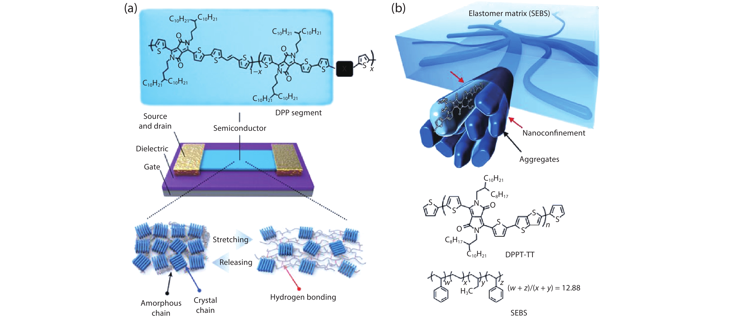
![(Color online) (a) Chemical structures of semiconducting polymers and mechanism for improved stretchability via dynamic bonding. (b) Schematic illustration of the embedded nanoscale polymer networks (top) and chemical structures of semiconducting polymer and elastomer (bottom). Panel (a) adapted with permission from Ref. [27]. Copyright 2016, Springer Nature. Panel (b) adapted with permission from Ref. [29]. Copyright 2017, American Association for the Advancement of Science.](/richHtml/jos/2020/41/4/041601/img_1.jpg)
Fig. 1. (Color online) (a) Chemical structures of semiconducting polymers and mechanism for improved stretchability via dynamic bonding. (b) Schematic illustration of the embedded nanoscale polymer networks (top) and chemical structures of semiconducting polymer and elastomer (bottom). Panel (a) adapted with permission from Ref. [27 ]. Copyright 2016, Springer Nature. Panel (b) adapted with permission from Ref. [29 ]. Copyright 2017, American Association for the Advancement of Science.
![(Color online) (a) Schematic illustration of the self-healing process of the polymer through reversible ion–dipole interactions. (b) Schematic illustration of the healing process of the treated polymer films (left) and transfer curves and mobility of the damaged and healed OTFTs (right). (c) Schematic of the self-healing composite of polymer networks and micro-nickel particles. Panel (a) adapted with permission from Ref. [47]. Copyright 2019, Springer Nature. Panel (b) adapted with permission from Ref. [27]. Copyright 2016, Springer Nature. Panel (c) adapted with permission from Ref. [53]. Copyright 2012, Springer Nature.](/richHtml/jos/2020/41/4/041601/img_2.jpg)
Fig. 2. (Color online) (a) Schematic illustration of the self-healing process of the polymer through reversible ion–dipole interactions. (b) Schematic illustration of the healing process of the treated polymer films (left) and transfer curves and mobility of the damaged and healed OTFTs (right). (c) Schematic of the self-healing composite of polymer networks and micro-nickel particles. Panel (a) adapted with permission from Ref. [47 ]. Copyright 2019, Springer Nature. Panel (b) adapted with permission from Ref. [27 ]. Copyright 2016, Springer Nature. Panel (c) adapted with permission from Ref. [53 ]. Copyright 2012, Springer Nature.
Fig. 3. (Color online) (a) Schematic of silicon-based transient electronics on silk substrate (top) and dissolution process in water (bottom). (b) Flexible devices with disintegrable polymers as the active material and substrate (left) and images of a device at various stages of disintegration (right). Panel (a) adapted with permission from Ref. [60 ]. Copyright 2012, American Association for the Advancement of Science. Panel (b) adapted with permission from Ref. [74 ]. Copyright 2017, National Academy of Sciences.
Fig. 4. (Color online) (a) The working mechanism of the CNT-based pressure and strain sensor (left) and the array design (right). (b) Schematic and image (inset) of a hierarchically pyramidal-structured pressure sensor. (c) The fabrication step of pressure-sensitive polymer transistor with a microstructured PDMS dielectric layer. (d) Schematic of a chameleon-inspired e-skin. (e) Images of a Si nanomembrane diode sensor array with magnified views of a single sensor. Panel (a) adapted with permission from Ref. [36 ]. Copyright 2011, Springer Nature. Panel (b) adapted with permission from Ref. [84 ]. Copyright 2017, IEEE. Panel (c) adapted with permission from Ref. [85 ]. Copyright 2013, Springer Nature. Panel (d) adapted with permission from Ref. [86 ]. Copyright 2015, Springer Nature. Panel (e) adapted with permission from Ref. [96 ]. Copyright 2013, Springer Nature.
Fig. 5. (Color online) (a) A photo (left) and structure (right) of a 300-nm-thick electronic skin, with an OFET and tactile sensor per pixel. (b) Schematic of a strain sensor array based on piezoelectric nanogenerators and coplanar-gate graphene transistors. (c) Images of intrinsically stretchable transistor array (left, scale bar: 1 mm), amplifier in its initial and stretched state (middle), and use of the amplifier for arterial pulse signal measurement. Panel (a) adapted with permission from Ref. [113 ]. Copyright 2016, Wiley. Panel (b) adapted with permission from Ref. [115 ]. Copyright 2015, Wiley. Panel (c) adapted with permission from Ref. [125 ]. Copyright 2018, Springer Nature.
Fig. 6. (Color online) (a) A multifunctional epidermal electronics (left) and its integration with tattoo. (b) Design of CNT TFT device (left) and photos of devices attached conformally to human skin (right). (c) Schematic illustration of a digital tactile system composed of flexible organic circuits. Panel (a) adapted with permission from Ref. [15 ]. Copyright 2011, American Association for the Advancement of Science. Panel (b) adapted with permission from Ref. [143 ]. Copyright 2019, Springer Nature. Panel (c) adapted with permission from Ref. [144 ]. Copyright 2015, American Association for the Advancement of Science.
Fig. 7. (Color online) (a) Schematic illustration (left) and photo (right) of a bodyNET with on-skin sensors and flexible circuits on clothes. (b) A piezoresistive sensor array consisting of 548 sensors covering the entire hand. (c) A self-healable electronic skin system composed of sensors and display. Panel (a) adapted with permission from Ref. [155 ]. Copyright 2019, Springer Nature. Panel (b) adapted with permission from Ref. [163 ]. Copyright 2019, Springer Nature. Panel (c) adapted with permission from Ref. [49 ]. Copyright 2018, Springer Nature.

Set citation alerts for the article
Please enter your email address


