
Zhong Ma, Desheng Kong, Lijia Pan, Zhenan Bao. Skin-inspired electronics: emerging semiconductor devices and systems[J]. Journal of Semiconductors, 2020, 41(4): 041601
- Journal of Semiconductors
- Vol. 41, Issue 4, 041601 (2020)
Abstract
1. Introduction
Skin is the largest organ featuring soft mechanical properties and a complex sensory network that interfaces with the environment, which serves as an inspiration for the development of next-generation flexible electronics[
To this end, skin-like properties including mechanical stretchability, self-healing capability, and biodegradability have been incorporated into new classes of electronic materials[
In this review, we focus on recent progress of skin-inspired electronics including material selection, device design, and system improvement. We summarize advances, with particular emphasis on semiconductor materials and devices. Several strategies for biomimetic sensors, and advanced system-level functional improvement along with applications in robots/prostheses, human-machine interfaces, and healthcare monitoring are discussed. We conclude with the remaining challenges and potential future directions of skin-inspired electronics.
2. Semiconducting materials with skin-like properties
Skin-like properties, including stretchability, self-healing capability, biocompatibility, and biodegradability, have been demonstrated in a new class of semiconductor materials to enable their wide application in skin-inspired electronics. These skin-like features are primarily based on new material concepts or innovative engineering approaches.
2.1. Stretchability
Typical biological skin has a modulus of 140–600 kPa and a maximal stretchability up to 75% tensile strain[
Strain engineering is a facile approach to enable stretchability in conventionally rigid and brittle materials. Inspired by wrinkles and creases of natural skin, geometry designs like kirigami, serpentine, buckling, and microcracks are utilized to create stretchable semiconducting materials[
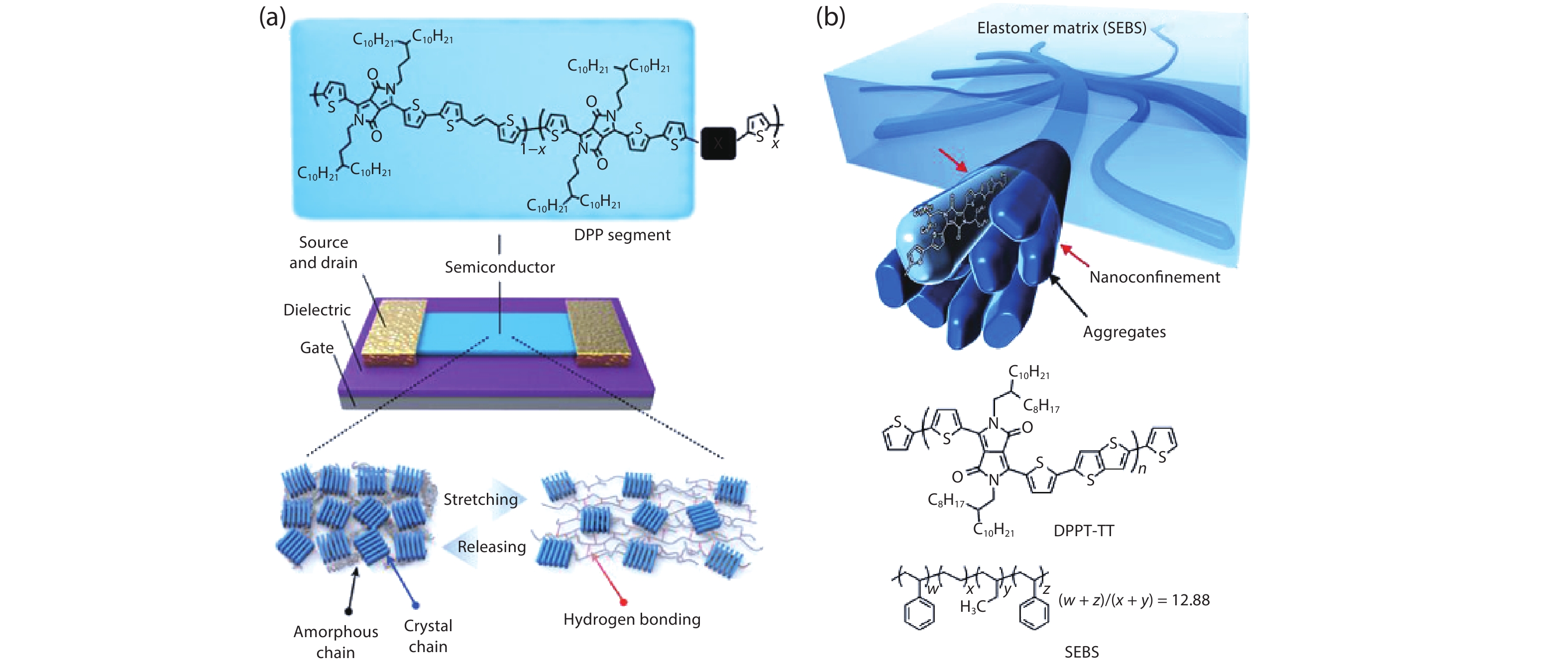
Intrinsically stretchable semiconducting materials can be stretched without degradation in their electronic performances, which is attractive for skin-inspired electronics to achieve stable and robust performances. Polymers are among the typical examples of stretchable semiconducting materials formed through standard solution processes[
![]()
Figure 1.(Color online) (a) Chemical structures of semiconducting polymers and mechanism for improved stretchability via dynamic bonding. (b) Schematic illustration of the embedded nanoscale polymer networks (top) and chemical structures of semiconducting polymer and elastomer (bottom). Panel (a) adapted with permission from Ref. [
Blending of functional nanomaterials into elastomers allows facile fabrication of stretchable composites with electrical conductivity and stable cycling[
2.2. Self-healing
Self-healing capability is a unique feature of natural skin to enable autonomous self-repair after damage[
Generally, self-healing capabilities are achieved through reversible bonds (e.g., hydrogen bonding or dynamic covalent bonding), dynamic interactions (e.g., host–guest interactions, π–π interactions, ionic interactions, and electrostatic interactions), and microcapsule-based composite with embedded self-healing agents[
![]()
Figure 2.(Color online) (a) Schematic illustration of the self-healing process of the polymer through reversible ion–dipole interactions. (b) Schematic illustration of the healing process of the treated polymer films (left) and transfer curves and mobility of the damaged and healed OTFTs (right). (c) Schematic of the self-healing composite of polymer networks and micro-nickel particles. Panel (a) adapted with permission from Ref. [
To realize fully self-healable devices, functional components with autonomous healing capabilities without any external stimuli are expected to be developed concurrently[
2.3. Biodegradability
Biodegradable materials are preferred in skin-inspired applications, which enable the devices to degrade into harmless components after their service life. It is essential for transdermal or implantable devices to avoid side effects for biomedical applications[
Biodegradable materials like metals (e.g., Mg, Zn, Mo, and Fe) and silicon-based technology is an interesting option for transient integrated devices with high hydrolysis rate but without any harmful products[
![]()
Figure 3.(Color online) (a) Schematic of silicon-based transient electronics on silk substrate (top) and dissolution process in water (bottom). (b) Flexible devices with disintegrable polymers as the active material and substrate (left) and images of a device at various stages of disintegration (right). Panel (a) adapted with permission from Ref. [
Decomposable conjugated polymers have emerged as another attractive choice for transient electronics[
Based on reversible imine chemistry, Lei et al. synthesized a biocompatible semiconducting polymer that is readily decomposable in mild acidic environments (Fig. 3(b))[
3. Skin-inspired devices and systems
Based on material selection and novel device design, artificial sensors imitating mechanisms and structures of natural skins, along with flexible circuits, are achieved. To go further beyond single-modal sensor unit, intelligent functionalities are incorporated to realize skin-like electronic devices and systems.
3.1. Sensors
Pressure sensing is a common and vital function to convert mechanical stimuli into electrical signals, which has been extensively studied. As an example, Lipomi et al. fabricated a transparent pressure and strain sensor based on elastic films of CNTs (Fig. 4(a))[
![]()
Figure 4.(Color online) (a) The working mechanism of the CNT-based pressure and strain sensor (left) and the array design (right). (b) Schematic and image (inset) of a hierarchically pyramidal-structured pressure sensor. (c) The fabrication step of pressure-sensitive polymer transistor with a microstructured PDMS dielectric layer. (d) Schematic of a chameleon-inspired e-skin. (e) Images of a Si nanomembrane diode sensor array with magnified views of a single sensor. Panel (a) adapted with permission from Ref. [
Schwartz et al. integrated microstructured PDMS dielectric with polymer transistor to amplify the capacitance responses and enable its operation in the subthreshold regime (Fig. 4(b))[
In natural skins, ionic mechanotransduction contributes to the conversion of mechanical stimuli into biochemical signals[
Temperature sensing is another vital function of the skin sensory system. Wearable skin thermography represents a complementary technology for traditional infrared imaging and point-contact sensors. Conventional measurement is typically based on temperature coefficient of resistance (TCR) that requires complicated readout circuits for amplification[
Considering that natural skin is responsive to various stimuli (e.g., pressure, strain, temperature, and humidity) simultaneously, multiplex sensors are desired for various wearable applications. Multimodal measurement can provide sufficient information to establish interconnections because some signals may be unavoidably affected by others[
Future efforts may be the integration of biochemical sensors into the skin system, which may target metabolites (e.g., glucose and lactate) and electrolytes (e.g., sodium and potassium ions)[
3.2. Transistors
Organic field-effect transistors (OFETs) represent the building blocks for complex circuit systems for skin-inspired electronics[
![]()
Figure 5.(Color online) (a) A photo (left) and structure (right) of a 300-nm-thick electronic skin, with an OFET and tactile sensor per pixel. (b) Schematic of a strain sensor array based on piezoelectric nanogenerators and coplanar-gate graphene transistors. (c) Images of intrinsically stretchable transistor array (left, scale bar: 1 mm), amplifier in its initial and stretched state (middle), and use of the amplifier for arterial pulse signal measurement. Panel (a) adapted with permission from Ref. [
A transistor-based matrix exhibits advantages in imitating skin that consists of thousands of sensory units due to advanced sensing performances, minimized scale, large-scale integration, and lower signal cross-talk as compared with simple resistive or capacitive sensors[
In addition to simply recording human vital signs, transistor-based sensing devices are also favorable for in-sensor signal processing, such as direct signal amplification and noise elimination[
Soft electronic devices have shown capabilities of acquiring high-quality biosignals due to the lowered interfacial impedance, reduced signal distortion, and high signal-to-noise ratio (SNR). Sugiyama et al. designed an ultraflexible organic differential amplifier for signal amplification and noise reduction, which allows the recording of weak electrocardiogram (ECG) signals with high signal integrity and sensitivity[
3.3. Circuit systems
For skin-inspired electronics, high-density functional circuits play an important part in signal collection, processing, and transmission, which pave the way for applications in implantable sensors, tissue engineering, and soft robotics[
The key challenges for the development of flexible circuit systems lie in thin-film interconnects and circuits compatible with flat encapsulations[
![]()
Figure 6.(Color online) (a) A multifunctional epidermal electronics (left) and its integration with tattoo. (b) Design of CNT TFT device (left) and photos of devices attached conformally to human skin (right). (c) Schematic illustration of a digital tactile system composed of flexible organic circuits. Panel (a) adapted with permission from Ref. [
In addition to the design of circuit layout, 3D integration is another efficient method to create stretchable electronic systems with complex functions[
In spite of the stretchability and flexibility for the overall system, the rigid island design has to deal with the complicated layout and fabrication process. The robustness of the circuit is often compromised by the weak interfaces between hard and soft components. Fully stretchable circuits based on compliant materials exhibit the inherent advantage in terms of the resilience[
3.4. Integrated skin-like functional systems
Skin-inspired electronics are attractive for various emerging fields such as wearable healthcare monitoring, soft robotics, and human–machine interface[
(1) Wireless data transmission
The trend for the next-generation electronic skin applications is developing wearable, on-demand, non-invasive, transdermal devices that detect physiological signals in real time[
![]()
Figure 7.(Color online) (a) Schematic illustration (left) and photo (right) of a bodyNET with on-skin sensors and flexible circuits on clothes. (b) A piezoresistive sensor array consisting of 548 sensors covering the entire hand. (c) A self-healable electronic skin system composed of sensors and display. Panel (a) adapted with permission from Ref. [
(2) Large-scale array
Electronic skin may serve as the enabler of tactile sensation for humanoid robots and prostheses[
Large-scale, high-resolution tactile datasets bring about abundant information for advanced signal processing tools such as machine learning[
(3) Closed-loops with feedback
For artificial intelligent electronic skin, sensory feedback is critical in building closed-loop control systems. For example, the effective and precise control of our hands largely rely on the sensory feedback and feedforward motor commands[
Another important step towards a smart electronic skin system is closed-loop system with instant smart drug delivery for point-of-care (PoC) healthcare applications[
4. Conclusion and outlook
In summary, we have reviewed recent progress in skin-inspired electronics from the aspect of semiconducting materials, sensor devices, and advanced systems. Inspired by the structures and mechanisms of living organisms, recent progress in soft materials and flexible electronics is beneficial for the achievement of skin-like materials and biomimetic sensors. An intelligent skin electronic system with advanced functions and capabilities like wireless data transmission, data collection of large-area arrays, and in-time feedback is explored to favor the real-world applications in fields such as wearable healthcare monitoring, human–machine interfaces, and smart robots/prostheses.
Several limitations still exist that require further studies including but not limited to the following aspects: (1) Enhancement of the functional characteristics. The flexibility, stretchability, biocompatibility, as well as sensing performances (including sensitivity, response speed, stability, anti-interference ability, and multimodal capability) need to be further improved for different application settings of wearable and implantable devices[
Acknowledgments
This work was supported by the National Natural Science Foundation of China under Grants 61825403, 61674078, and 61921005, the National Key Research and Development program of China under Grant 2017YFA0206302, and the PAPD program.
References
[1] S Wang, J Y Oh, J Xu et al. Skin-inspired electronics: an emerging paradigm. Acc Chem Res, 51, 1033(2018).
[2] J C Yang, J Mun, S Y Kwon et al. Electronic skin: recent progress and future prospects for skin-attachable devices for health monitoring, robotics, and prosthetics. Adv Mater, 1904765(2019).
[3] M L Hammock, A Chortos, B C K Tee et al. The evolution of electronic skin (E-Skin): A brief history, design considerations, and recent progress. Adv Mater, 25, 5997(2013).
[4] Z Ma, S Li, H Wang et al. Advanced electronic skin devices for healthcare applications. J Mater Chem B, 7, 173(2019).
[5] L Wang, D Chen, K Jiang et al. New insights and perspectives into biological materials for flexible electronics. Chem Soc Rev, 46, 6764(2017).
[6] T Li, Y Li, T Zhang. Materials, structures, and functions for flexible and stretchable biomimetic sensors. Acc Chem Res, 52, 288(2019).
[7] Y Liu, K He, G Chen et al. Nature-inspired structural materials for flexible electronic devices. Chem Rev, 117, 12893(2017).
[8] K Wang, Z Lou, L Wang et al. Bioinspired interlocked structure-induced high deformability for two-dimensional titanium carbide (MXene)/natural microcapsule-based flexible pressure sensors. ACS Nano, 13, 9139(2019).
[9] A Chortos, J Liu, Z Bao. Pursuing prosthetic electronic skin. Nat Mater, 15, 937(2016).
[10] J Li, Z Ma, H Wang et al. Skin-inspired electronics and its applications in advanced intelligent systems. Adv Intell Syst, 0, 1900063(2019).
[11] Z Lou, L Wang, G Shen. Recent advances in smart wearable sensing systems. Adv Mater Technol, 3, 1800444(2018).
[12] S Yao, P Swetha, Y Zhu. Nanomaterial-enabled wearable sensors for healthcare. Adv Healthc Mater, 7, 1700889(2018).
[13] C Edwards, R Marks. Evaluation of biomechanical properties of human skin. Clin Dermatol, 13, 375(1995).
[14] Y Liu, M Pharr, G A Salvatore. Lab-on-skin: A review of flexible and stretchable electronics for wearable health monitoring. ACS Nano, 11, 9614(2017).
[15] D H Kim, N Lu, R Ma et al. Epidermal electronics. Science, 333, 838(2011).
[16] A J Bandodkar, I Jeerapan, J M You et al. Highly stretchable fully-printed CNT-based electrochemical sensors and biofuel cells: combining intrinsic and design-induced stretchability. Nano Lett, 16, 721(2016).
[17] T C Shyu, P F Damasceno, P M Dodd et al. A kirigami approach to engineering elasticity in nanocomposites through patterned defects. Nat Mater, 14, 785(2015).
[18] H Vandeparre, Q Liu, I R Minev et al. Localization of folds and cracks in thin metal films coated on flexible elastomer foams. Adv Mater, 25, 3117(2013).
[19] K Li, X Cheng, F Zhu et al. A generic soft encapsulation strategy for stretchable electronics. Adv Funct Mater, 29, 1806630(2019).
[20] J Li, E Song, C H Chiang et al. Conductively coupled flexible silicon electronic systems for chronic neural electrophysiology. Proc Natl Acad Sci, 115, E9542(2018).
[21] W Cheng, L Yu, D Kong et al. Fast-response and low-hysteresis flexible pressure sensor based on silicon nanowires. IEEE Electron Device Lett, 39, 1069(2018).
[22] Y Wang, C Zhu, R Pfattner et al. A highly stretchable, transparent, and conductive polymer. Sci Adv, 3, e1602076(2017).
[23] R Nur, N Matsuhisa, Z Jiang et al. A highly sensitive capacitive-type strain sensor using wrinkled ultrathin gold films. Nano Lett, 18, 5610(2018).
[24] C Müller, S Goffri, D W Breiby et al. Tough, semiconducting polyethylene-poly(3-hexylthiophene) diblock copolymers. Adv Funct Mater, 17, 2674(2007).
[25] B O’Connor, R J Kline, B R Conrad et al. Anisotropic structure and sharge transport in highly strain-aligned regioregular poly(3-hexylthiophene). Adv Funct Mater, 21, 3697(2011).
[26] G J N Wang, L Shaw, J Xu et al. Inducing elasticity through oligo-siloxane crosslinks for intrinsically stretchable semiconducting polymers. Adv Funct Mater, 26, 7254(2016).
[27] J Y Oh, S Rondeau-Gagné, Y C Chiu et al. Intrinsically stretchable and healable semiconducting polymer for organic transistors. Nature, 539, 411(2016).
[28] L Si, M V Massa, K Dalnoki-Veress et al. Chain entanglement in thin freestanding polymer films. Phys Rev Lett, 94, 127801(2005).
[29] J Xu, S Wang, G J N Wang et al. Highly stretchable polymer semiconductor films through the nanoconfinement effect. Science, 355, 59(2017).
[30] Y Kim, J Zhu, B Yeom et al. Stretchable nanoparticle conductors with self-organized conductive pathways. Nature, 500, 59(2013).
[31] T Q Trung, N E Lee. Recent progress on stretchable electronic devices with intrinsically stretchable components. Adv Mater, 29, 1603167(2017).
[32] Z Ma, W Shi, K Yan et al. Doping engineering of conductive polymer hydrogels and their application in advanced sensor technologies. Chem Sci, 10, 6232(2019).
[33] E Song, B Kang, H H Choi et al. Stretchable and transparent organic semiconducting thin film with conjugated polymer nanowires embedded in an elastomeric matrix. Adv Electron Mater, 2, 1500250(2016).
[34] Y Zhang, C J Sheehan, J Zhai et al. Polymer-embedded carbon nanotube ribbons for stretchable conductors. Adv Mater, 22, 3027(2010).
[35] T Q Trung, S Ramasundaram, B U Hwang et al. An all-elastomeric transparent and stretchable temperature sensor for body-attachable wearable electronics. Adv Mater, 28, 502(2016).
[36] D J Lipomi, M Vosgueritchian, B C K Tee et al. Skin-like pressure and strain sensors based on transparent elastic films of carbon nanotubes. Nat Nanotechnol, 6, 788(2011).
[37] J Liang, L Li, D Chen et al. Intrinsically stretchable and transparent thin-film transistors based on printable silver nanowires, carbon nanotubes and an elastomeric dielectric. Nat Commun, 6, 7647(2015).
[38] S Chen, K Jiang, Z Lou et al. Recent developments in graphene-based tactile sensors and E-skins. Adv Mater Technol, 3, 1700248(2018).
[39] C Wang, H Wu, Z Chen et al. Self-healing chemistry enables the stable operation of silicon microparticle anodes for high-energy lithium-ion batteries. Nat Chem, 5, 1042(2013).
[40] A J Bandodkar, V Mohan, C S López et al. Self-healing inks for autonomous repair of printable electrochemical devices. Adv Electron Mater, 1, 1500289(2015).
[41] T Wang, Y Zhang, Q Liu et al. A self-healable, highly stretchable, and solution processable conductive polymer composite for ultrasensitive strain and pressure sensing. Adv Funct Mater, 28, 1705551(2018).
[42] W Pu, F Jiang, P Chen et al. A POSS based hydrogel with mechanical robustness, cohesiveness and a rapid self-healing ability by electrostatic interaction. Soft Matter, 13, 5645(2017).
[43] M Nakahata, Y Takashima, A Harada. Highly flexible, tough, and self-healing supramolecular polymeric materials using host–guest interaction. Macromol Rapid Commun, 37, 86(2016).
[44] J Kang, D Son, G J N Wang et al. Tough and water-insensitive self-healing elastomer for robust electronic skin. Adv Mater, 30, 1706846(2018).
[45] G J N Wang, A Gasperini, Z Bao. Stretchable polymer semiconductors for plastic electronics. Adv Electron Mater, 4, 1700429(2018).
[46] C H Li, C Wang, C Keplinger et al. A highly stretchable autonomous self-healing elastomer. Nat Chem, 8, 618(2016).
[47] Y Cao, Y J Tan, S Li et al. Self-healing electronic skins for aquatic environments. Nat Electron, 2, 75(2019).
[48] J Kang, J B H Tok, Z Bao. Self-healing soft electronics. Nat Electron, 2, 144(2019).
[49] D Son, J Kang, O Vardoulis et al. An integrated self-healable electronic skin system fabricated via dynamic reconstruction of a nanostructured conducting network. Nat Nanotechnol, 13, 1057(2018).
[50] K Guo, D L Zhang, X M Zhang et al. Conductive elastomers with autonomic self-healing properties. Angew Chem Int Ed, 54, 12127(2015).
[51] E D’Elia, S Barg, N Ni et al. Self-healing graphene-based composites with sensing capabilities. Adv Mater, 27, 4788(2015).
[52] X Yan, Z Liu, Q Zhang et al. Quadruple H-bonding cross-linked supramolecular polymeric materials as substrates for stretchable, antitearing, and self-healable thin film electrodes. J Am Chem Soc, 140, 5280(2018).
[53] B C K Tee, C Wang, R Allen et al. An electrically and mechanically self-healing composite with pressure-and flexion-sensitive properties for electronic skin applications. Nat Nanotechnol, 7, 825(2012).
[54] M Khatib, T P Huynh, Y Deng et al. A freestanding stretchable and multifunctional transistor with intrinsic self-healing properties of all device components. Small, 15, 1803939(2019).
[55] T Dvir, B P Timko, M D Brigham et al. Nanowired three-dimensional cardiac patches. Nat Nanotechnol, 6, 720(2011).
[56] C J Bettinger, Z Bao. Organic thin-film transistors fabricated on resorbable biomaterial substrates. Adv Mater, 22, 651(2010).
[57] G A Salvatore, J Sülzle, Valle F Dalla et al. Biodegradable and highly deformable temperature sensors for the internet of things. Adv Funct Mater, 27, 1702390(2017).
[58] S W Hwang, G Park, H Cheng et al. Materials for high-performance biodegradable semiconductor devices. Adv Mater, 26, 1992(2014).
[59] D Lu, T L Liu, J K Chang et al. Transient light-emitting diodes constructed from semiconductors and transparent conductors that biodegrade under physiological conditions. Adv Mater, 31, 1902739(2019).
[60] S W Hwang, H Tao, D H Kim et al. A physically transient form of silicon electronics. Science, 337, 1640(2012).
[61] S W Hwang, C H Lee, H Cheng et al. Biodegradable elastomers and silicon nanomembranes/nanoribbons for stretchable, transient electronics, and biosensors. Nano Lett, 15, 2801(2015).
[62] S W Hwang, X Huang, J H Seo et al. Materials for bioresorbable radio frequency electronics. Adv Mater, 25, 3526(2013).
[63] S K Kang, R K J Murphy, S W Hwang et al. Bioresorbable silicon electronic sensors for the brain. Nature, 530, 71(2016).
[64] W Bai, J Shin, R Fu et al. Bioresorbable photonic devices for the spectroscopic characterization of physiological status and neural activity. Nat Biomed Eng, 3, 644(2019).
[65] J Shin, Z Liu, W Bai et al. Bioresorbable optical sensor systems for monitoring of intracranial pressure and temperature. Sci Adv, 5, eaaw1899(2019).
[66] T Lei, X Chen, G Pitner et al. Removable and recyclable conjugated polymers for highly selective and high-yield dispersion and release of low-cost carbon nanotubes. J Am Chem Soc, 138, 802(2016).
[67] M Irimia-Vladu, P A Troshin, M Reisinger et al. Biocompatible and biodegradable materials for organic field-effect transistors. Adv Funct Mater, 20, 4069(2010).
[68] M Irimia-Vladu, E D Głowacki, P A Troshin et al. Indigo-a natural pigment for high performance ambipolar organic field effect transistors and circuits. Adv Mater, 24, 375(2012).
[69] L Wang, K Wang, Z Lou et al. Plant-based modular building blocks for “green” electronic skins. Adv Funct Mater, 28, 1804510(2018).
[70] C Wang, X Li, E Gao et al. Carbonized silk fabric for ultrastretchable, highly sensitive, and wearable strain sensors. Adv Mater, 28, 6640(2016).
[71] C Wang, K Xia, M Zhang et al. An all-silk-derived dual-mode e-skin for simultaneous temperature–pressure detection. ACS Appl Mater Interfaces, 9, 39484(2017).
[72] C M Boutry, Y Kaizawa, B C Schroeder et al. A stretchable and biodegradable strain and pressure sensor for orthopaedic application. Nat Electron, 1, 314(2018).
[73] D Khodagholy, J N Gelinas, T Thesen et al. NeuroGrid: recording action potentials from the surface of the brain. Nat Neurosci, 18, 310(2015).
[74] T Lei, M Guan, J Liu et al. Biocompatible and totally disintegrable semiconducting polymer for ultrathin and ultralightweight transient electronics. Proc Natl Acad Sci, 114, 5107(2017).
[75] C M Boutry, L Beker, Y Kaizawa et al. Biodegradable and flexible arterial-pulse sensor for the wireless monitoring of blood flow. Nat Biomed Eng, 3, 47(2019).
[76] S C B Mannsfeld, B C K Tee, R M Stoltenberg et al. Highly sensitive flexible pressure sensors with microstructured rubber dielectric layers. Nat Mater, 9, 859(2010).
[77] C M Boutry, M Negre, M Jorda et al. A hierarchically patterned, bioinspired e-skin able to detect the direction of applied pressure for robotics. Sci Robot, 3, eaau6914(2018).
[78] Z W K Low, Z Li, C Owh et al. Using artificial skin devices as skin replacements: insights into superficial treatment. Small, 15, 1805453(2019).
[79] C M Boutry, A Nguyen, Q O Lawal et al. A sensitive and biodegradable pressure sensor array for cardiovascular monitoring. Adv Mater, 27, 6954(2015).
[80] B C K Tee, A Chortos, R R Dunn et al. Tunable flexible pressure sensors using microstructured elastomer geometries for intuitive electronics. Adv Funct Mater, 24, 5427(2014).
[81] G Y Bae, J T Han, G Lee et al. Pressure/temperature sensing bimodal electronic skin with stimulus discriminability and linear sensitivity. Adv Mater, 30, 1803388(2018).
[82] Z Wang, S Guo, H Li et al. The semiconductor/conductor interface piezoresistive effect in an organic transistor for highly sensitive pressure sensors. Adv Mater, 31, 1805630(2019).
[83] S H Cho, S W Lee, S Yu et al. Micropatterned pyramidal ionic gels for sensing broad-range pressures with high sensitivity. ACS Appl Mater Interfaces, 9, 10128(2017).
[84] G Schwartz, B C K Tee, J Mei et al. Flexible polymer transistors with high pressure sensitivity for application in electronic skin and health monitoring. Nat Commun, 4, 1859(2013).
[85] W Cheng, J Wang, Z Ma et al. Flexible pressure sensor with high sensitivity and low hysteresis based on a hierarchically microstructured electrode. IEEE Electron Device Lett, 39, 288(2018).
[86] H H Chou, A Nguyen, A Chortos et al. A chameleon-inspired stretchable electronic skin with interactive colour changing controlled by tactile sensing. Nat Commun, 6, 8011(2015).
[87] L Pan, A Chortos, G Yu et al. An ultra-sensitive resistive pressure sensor based on hollow-sphere microstructure induced elasticity in conducting polymer film. Nat Commun, 5, 3002(2014).
[88] G Y Bae, S W Pak, D Kim et al. Linearly and highly pressure-sensitive electronic skin based on a bioinspired hierarchical structural array. Adv Mater, 28, 5300(2016).
[89] C Pang, G Y Lee, T Kim et al. A flexible and highly sensitive strain-gauge sensor using reversible interlocking of nanofibres. Nat Mater, 11, 795(2012).
[90] D Kang, P V Pikhitsa, Y W Choi et al. Ultrasensitive mechanical crack-based sensor inspired by the spider sensory system. Nature, 516, 222(2014).
[91] S S Ranade, R Syeda, A Patapoutian. Mechanically activated ion channels. Neuron, 87, 1162(2015).
[92] K Schrenk-Siemens, H Wende, V Prato et al. PIEZO2 is required for mechanotransduction in human stem cell–derived touch receptors. Nat Neurosci, 18, 10(2015).
[93] M L Jin, S Park, Y Lee et al. An ultrasensitive, visco-poroelastic artificial mechanotransducer skin inspired by piezo2 protein in mammalian merkel cells. Adv Mater, 29, 1605973(2017).
[94] C Y Lee, G W Wu, W J Hsieh. Fabrication of micro sensors on a flexible substrate. Sens Actuators Phys, 147, 173(2008).
[95] I Y Han, S J Kim. Diode temperature sensor array for measuring micro-scale surface temperatures with high resolution. Sens Actuators Phys, 141, 52(2008).
[96] R C Webb, A P Bonifas, A Behnaz et al. Ultrathin conformal devices for precise and continuous thermal characterization of human skin. Nat Mater, 12, 938(2013).
[97] J Jeon, H B Lee, Z Bao. Flexible wireless temperature sensors based on Ni microparticle-filled binary polymer composites. Adv Mater, 25, 850(2013).
[98] W H Yeo, Y S Kim, J Lee et al. Multifunctional epidermal electronics printed directly onto the skin. Adv Mater, 25, 2773(2013).
[99] A Chortos, Z Bao. Skin-inspired electronic devices. Mater Today, 17, 321(2014).
[100] S Zhao, R Zhu. Flexible bimodal sensor for simultaneous and independent perceiving of pressure and temperature stimuli. Adv Mater Technol, 2, 1700183(2017).
[101] D H Ho, Q Sun, S Y Kim et al. Stretchable and multimodal all graphene electronic skin. Adv Mater, 28, 2601(2016).
[102] Q Wang, M Jian, C Wang et al. Carbonized silk nanofiber membrane for transparent and sensitive electronic skin. Adv Funct Mater, 27, 1605657(2017).
[103] W Gao, S Emaminejad, H Y Y Nyein et al. Fully integrated wearable sensor arrays for multiplexed in situ perspiration analysis. Nature, 529, 509(2016).
[104] R J Sempionatto, T Nakagawa, A Pavinatto et al. Eyeglasses based wireless electrolyte and metabolite sensor platform. Lab Chip, 17, 1834(2017).
[105] L Wang, Z Lou, K Jiang et al. Bio-multifunctional smart wearable sensors for medical devices. Adv Intell Syst, 0, 1900040(2019).
[106] T Yokota, T Sekitani, T Tokuhara et al. Sheet-type flexible organic active matrix amplifier system using pseudo-CMOS circuits with floating-gate structure. IEEE Trans Electron Devices, 59, 3434(2012).
[107] K Ishida, T Huang, K Honda et al. Insole pedometer with piezoelectric energy harvester and 2 V organic circuits. IEEE J Solid-State Circuits, 48, 255(2013).
[108] X Ji, P Zhou, L Zhong et al. Smart surgical catheter for C-reactive protein sensing based on an imperceptible organic transistor. Adv Sci, 5, 1701053(2018).
[109] A Chortos, G I Koleilat, R Pfattner et al. Mechanically durable and highly stretchable transistors employing carbon nanotube semiconductor and electrodes. Adv Mater, 28, 4441(2016).
[110] J Viventi, D H Kim, L Vigeland et al. Flexible, foldable, actively multiplexed, high-density electrode array for mapping brain activity in vivo. Nat Neurosci, 14, 1599(2011).
[111] D Kong, R Pfattner, A Chortos et al. Capacitance characterization of elastomeric dielectrics for applications in intrinsically stretchable thin film transistors. Adv Funct Mater, 26, 4680(2016).
[112] A Chortos, J Lim, J W F To et al. Highly stretchable transistors using a microcracked organic semiconductor. Adv Mater, 26, 4253(2014).
[113] R A Nawrocki, N Matsuhisa, T Yokota et al. 300-nm imperceptible, ultraflexible, and biocompatible e-skin fit with tactile sensors and organic transistors. Adv Electron Mater, 2, 1500452(2016).
[114] S Lee, A Reuveny, J Reeder et al. A transparent bending-insensitive pressure sensor. Nat Nanotechnol, 11, 472(2016).
[115] Q Sun, W Seung, B J Kim et al. Active matrix electronic skin strain sensor based on piezopotential-powered graphene transistors. Adv Mater, 27, 3411(2015).
[116] T Someya, T Sekitani, S Iba et al. A large-area, flexible pressure sensor matrix with organic field-effect transistors for artificial skin applications. Proc Natl Acad Sci, 101, 9966(2004).
[117] R Pfattner, A M Foudeh, C Liong et al. On the working mechanisms of solid-state double-layer-dielectric-based organic field-effect transistors and their implication for sensors. Adv Electron Mater, 4, 1700326(2018).
[118] R Pfattner, A M Foudeh, S Chen et al. Dual-gate organic field-effect transistor for pH sensors with tunable sensitivity. Adv Electron Mater, 5, 1800381(2019).
[119] C Zhu, H C Wu, G Nyikayaramba et al. Intrinsically stretchable temperature sensor based on organic thin-film transistors. IEEE Electron Device Lett, 40, 1630(2019).
[120] Q Sun, D H Kim, S S Park et al. Transparent, low-power pressure sensor matrix based on coplanar-gate graphene transistors. Adv Mater, 26, 4735(2014).
[121] T Sekitani, T Yokota, K Kuribara et al. Ultraflexible organic amplifier with biocompatible gel electrodes. Nat Commun, 7, 1(2016).
[122] A Reuveny, S Lee, T Yokota et al. High-frequency, conformable organic amplifiers. Adv Mater, 28, 3298(2016).
[123] N Matsuhisa, Y Jiang, Z Liu et al. High-transconductance stretchable transistors achieved by controlled gold microcrack morphology. Adv Electron Mater, 5, 1900347(2019).
[124] F Molina-Lopez, T Z Gao, U Kraft et al. Inkjet-printed stretchable and low voltage synaptic transistor array. Nat Commun, 10, 1(2019).
[125] S Wang, J Xu, W Wang et al. Skin electronics from scalable fabrication of an intrinsically stretchable transistor array. Nature, 555, 83(2018).
[126] M Sugiyama, T Uemura, M Kondo et al. An ultraflexible organic differential amplifier for recording electrocardiograms. Nat Electron, 2, 351(2019).
[127] H Lee, S Lee, W Lee et al. Ultrathin organic electrochemical transistor with nonvolatile and thin gel electrolyte for long-term electrophysiological monitoring. Adv Funct Mater, 1906982(2019).
[128] M Uz, K Jackson, M S Donta et al. Fabrication of high-resolution graphene-based flexible electronics via polymer casting. Sci Rep, 9, 10595(2019).
[129] S C Liu, T Delbruck. Neuromorphic sensory systems. Curr Opin Neurobiol, 20, 288(2010).
[130] C Zhu, A Chortos, Y Wang et al. Stretchable temperature-sensing circuits with strain suppression based on carbon nanotube transistors. Nat Electron, 1, 183(2018).
[131] A K K Kyaw, H H C Loh, F Yan et al. A polymer transistor array with a pressure-sensitive elastomer for electronic skin. J Mater Chem C, 5, 12039(2017).
[132] J Kim, D Son, M Lee et al. A wearable multiplexed silicon nonvolatile memory array using nanocrystal charge confinement. Sci Adv, 2, e1501101(2016).
[133] H Wang, P Wei, Y Li et al. Tuning the threshold voltage of carbon nanotube transistors by n-type molecular doping for robust and flexible complementary circuits. Proc Natl Acad Sci, 111, 4776(2014).
[134] J Kim, A Banks, H Cheng et al. Epidermal electronics with advanced capabilities in near-field communication. Small, 11, 906(2015).
[135] J Kim, A Banks, Z Xie et al. Miniaturized flexible electronic systems with wireless power and near-field communication capabilities. Adv Funct Mater, 25, 4761(2015).
[136] A Miyamoto, S Lee, N F Cooray et al. Inflammation-free, gas-permeable, lightweight, stretchable on-skin electronics with nanomeshes. Nat Nanotechnol, 12, 907(2017).
[137] L Tian, B Zimmerman, A Akhtar et al. Large-area MRI-compatible epidermal electronic interfaces for prosthetic control and cognitive monitoring. Nat Biomed Eng, 3, 194(2019).
[138] Y Zhang, H Fu, S Xu et al. A hierarchical computational model for stretchable interconnects with fractal-inspired designs. J Mech Phys Solids, 72, 115(2014).
[139] Z Huang, Y Hao, Y Li et al. Three-dimensional integrated stretchable electronics. Nat Electron, 1, 473(2018).
[140] B Xu, A Akhtar, Y Liu et al. An epidermal stimulation and sensing platform for sensorimotor prosthetic control, management of lower back exertion, and electrical muscle activation. Adv Mater, 28, 4462(2016).
[141] H Chen, Y Cao, J Zhang et al. Large-scale complementary macroelectronics using hybrid integration of carbon nanotubes and IGZO thin-film transistors. Nat Commun, 5, 4097(2014).
[142] H E Lee, S Kim, J Ko et al. Skin-like oxide thin-film transistors for transparent displays. Adv Funct Mater, 26, 6170(2016).
[143] T Lei, L L Shao, Y Q Zheng et al. Low-voltage high-performance flexible digital and analog circuits based on ultrahigh-purity semiconducting carbon nanotubes. Nat Commun, 10, 2161(2019).
[144] B C K Tee, A Chortos, A Berndt et al. A skin-inspired organic digital mechanoreceptor. Science, 350, 313(2015).
[145] C Yeom, K Chen, D Kiriya et al. Large-area compliant tactile sensors using printed carbon nanotube active-matrix backplanes. Adv Mater, 27, 1561(2015).
[146] T Sekitani, T Yokota, U Zschieschang et al. Organic nonvolatile memory transistors for flexible sensor arrays. Science, 326, 1516(2009).
[147] C Bartolozzi, L Natale, F Nori et al. Robots with a sense of touch. Nat Mater, 15, 921(2016).
[148] J Kim, J R Sempionatto, S Imani et al. Simultaneous monitoring of sweat and interstitial fluid using a single wearable biosensor platform. Adv Sci, 5, 1800880(2018).
[149] H Lee, C Song, S Baik et al. Device-assisted transdermal drug delivery. Adv Drug Deliv Rev, 127, 35(2018).
[150] H U Chung, B H Kim, J Y Lee et al. Binodal, wireless epidermal electronic systems with in-sensor analytics for neonatal intensive care. Science, 363, eaau0780(2019).
[151] Z Ma, P Chen, W Cheng et al. Highly sensitive, printable nanostructured conductive polymer wireless sensor for food spoilage detection. Nano Lett, 18, 4570(2018).
[152] A J Bandodkar, P Gutruf, J Choi et al. Battery-free, skin-interfaced microfluidic/electronic systems for simultaneous electrochemical, colorimetric, and volumetric analysis of sweat. Sci Adv, 5, eaav3294(2019).
[153] Z Cao, P Chen, Z Ma et al. Near-field communication sensors. Sensors, 19, 3947(2019).
[154] L Y Chen, B C K Tee, A L Chortos et al. Continuous wireless pressure monitoring and mapping with ultra-small passive sensors for health monitoring and critical care. Nat Commun, 5, 5028(2014).
[155] S Niu, N Matsuhisa, L Beker et al. A wireless body area sensor network based on stretchable passive tags. Nat Electron, 2, 361(2019).
[156] P Maiolino, M Maggiali, G Cannata et al. A flexible and robust large scale capacitive tactile system for robots. IEEE Sens J, 13, 3910(2013).
[157] M Liu, X Pu, C Jiang et al. Large-area all-textile pressure sensors for monitoring human motion and physiological signals. Adv Mater, 29, 1703700(2017).
[158] X Wu, Y Han, X Zhang et al. Large-area compliant, low-cost, and versatile pressure-sensing platform based on microcrack-designed carbon black@polyurethane sponge for human−machine interfacing. Adv Funct Mater, 26, 6246(2016).
[159] J Kim, M Lee, H J Shim et al. Stretchable silicon nanoribbon electronics for skin prosthesis. Nat Commun, 5, 5747(2014).
[160] J Viventi, D H Kim, J D Moss et al. A conformal, bio-interfaced class of silicon electronics for mapping cardiac electrophysiology. Sci Trans Med, 2, 24ra22(2010).
[161] Y J Park, B K Sharma, S M Shinde et al. All MoS2-based large area, skin-attachable active-matrix tactile sensor. ACS Nano, 13, 3023(2019).
[162] S K Kim, E A Kirchner, A Stefes et al. Intrinsic interactive reinforcement learning – Using error-related potentials for real world human-robot interaction. Sci Rep, 7, 1(2017).
[163] S Sundaram, P Kellnhofer, Y Li et al. Learning the signatures of the human grasp using a scalable tactile glove. Nature, 569, 698(2019).
[164] M Markovic, M A Schweisfurth, L F Engels et al. Myocontrol is closed-loop control: incidental feedback is sufficient for scaling the prosthesis force in routine grasping. J NeuroEngineering Rehabil, 15, 81(2018).
[165] A P Gerratt, H O Michaud, S P Lacour. Elastomeric electronic skin for prosthetic tactile sensation. Adv Funct Mater, 25, 2287(2015).
[166] X Jin, D D Zhu, B Z Chen et al. Insulin delivery systems combined with microneedle technology. Adv Drug Deliv Rev, 127, 119(2018).
[167] E K W Tan, Y Z Au, G K Moghaddam et al. Towards closed-loop integration of point-of-care technologies. Trends Biotechnol, 37, 775(2019).
[168] H Lee, T K Choi, Y B Lee et al. A graphene-based electrochemical device with thermoresponsive microneedles for diabetes monitoring and therapy. Nat Nanotechnol, 11, 566(2016).
[169] Y Zhang, J Wang, J Yu et al. Bioresponsive microneedles with a sheath structure for H2O2 and pH cascade-triggered insulin delivery. Small, 14, 1704181(2018).
[170] H Lee, C Song, Y S Hong et al. Wearable/disposable sweat-based glucose monitoring device with multistage transdermal drug delivery module. Sci Adv, 3, e1601314(2017).
[171] Z Tong, J Zhou, J Zhong et al. Glucose-and H2O2-responsive polymeric vesicles integrated with microneedle patches for glucose-sensitive transcutaneous delivery of insulin in diabetic rats. ACS Appl Mater Interfaces, 10, 20014(2018).
[172] A Koh, D Kang, Y Xue et al. A soft, wearable microfluidic device for the capture, storage, and colorimetric sensing of sweat. Sci Trans Med, 8, 366ra165(2016).
[173] J Yu, Y Zhang, Y Ye et al. Microneedle-array patches loaded with hypoxia-sensitive vesicles provide fast glucose-responsive insulin delivery. Proc Natl Acad Sci, 112, 8260(2015).
[174] I R Minev, P Musienko, A Hirsch et al. Electronic dura mater for long-term multimodal neural interfaces. Science, 347, 159(2015).
[175] L Li, L Pan, Z Ma et al. All inkjet-printed amperometric multiplexed biosensors based on nanostructured conductive hydrogel electrodes. Nano Lett, 18, 3322(2018).
[176] S Fu, J Tao, W Wu et al. Fabrication of large-area bimodal sensors by all-inkjet-printing. Adv Mater Technol, 4, 1800703(2019).

Set citation alerts for the article
Please enter your email address
© Copyright 2018-2021 | Chinese Laser Press. All Rights Reserved 沪ICP备15018463号-20