• Laser & Optoelectronics Progress
  • Vol. 59, Issue 19, 1913002 (2022)
Qiang Huang1、2, Yi Zhang1, Peilin Jiang1, Changliang Yu3, Haotian Shi1, Chukun Huang1, and Junqiang Sun1、*
Author Affiliations
  • 1Wuhan National Laboratory for Optoelectronics, Huazhong University of Science and Technology, Wuhan 430074, Hubei, China
  • 2Hunan Province Key Laboratory of Grids Operation and Control on Multi-Power Sources Area, School of Electrical Engineering, Shaoyang University, Shaoyang 422000, Hunan, China
  • 3Wuhan Fisilink Microelectronics Technology Co., Ltd., Wuhan 430040, Hubei, China
  • show less
    DOI: 10.3788/LOP202259.1913002 Cite this Article Set citation alerts
    Qiang Huang, Yi Zhang, Peilin Jiang, Changliang Yu, Haotian Shi, Chukun Huang, Junqiang Sun. Research on High-Efficiency Coupling Gratings Applied to Silicon Germanium Materials[J]. Laser & Optoelectronics Progress, 2022, 59(19): 1913002 Copy Citation Text show less
    Structure and cross-section of SiGe grating coupler
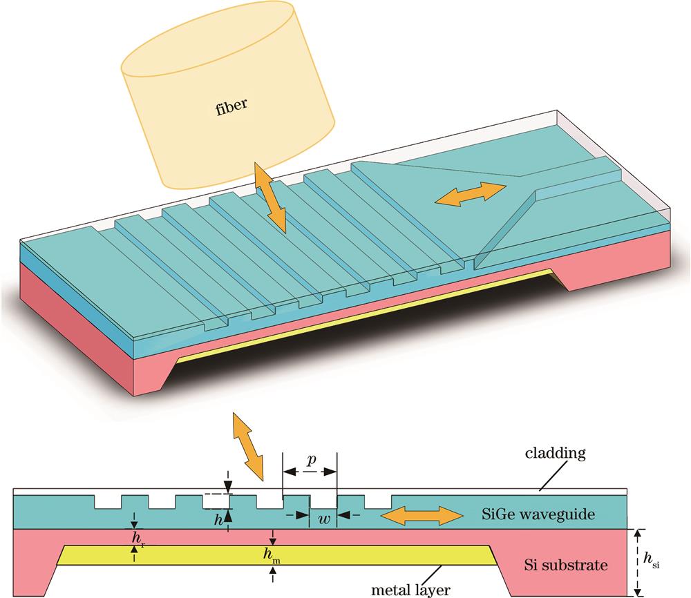
    Fig. 1. Structure and cross-section of SiGe grating coupler
    Relationship between coupling efficiency, etch depth, and operating wavelength
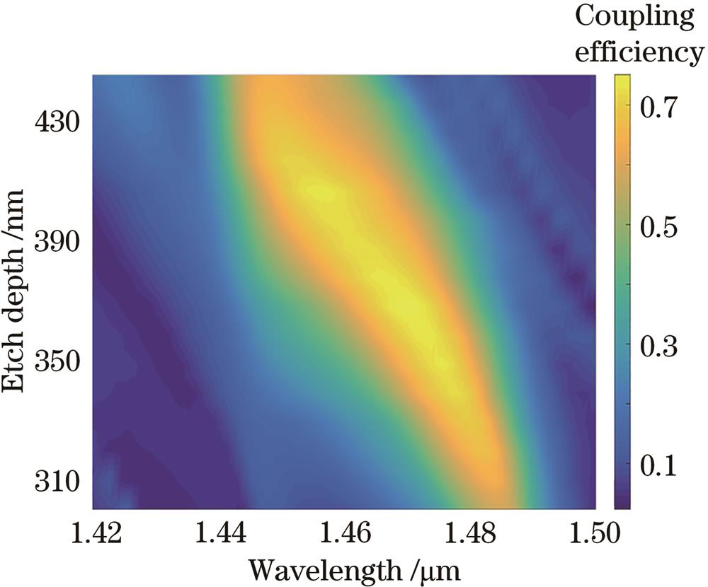
    Fig. 2. Relationship between coupling efficiency, etch depth, and operating wavelength
    Coupling efficiency spectra of SiGe grating with and without metal reflective layer
    Fig. 3. Coupling efficiency spectra of SiGe grating with and without metal reflective layer
    Simulation results of SiGe grating with and without metal reflective layer. (a) Simulated electric field distribution; (b) simulated optical power distribution
    Fig. 4. Simulation results of SiGe grating with and without metal reflective layer. (a) Simulated electric field distribution; (b) simulated optical power distribution
    Coupling efficiency spectra of uniform SiGe gratings and two-step apodized SiGe grating
    Fig. 5. Coupling efficiency spectra of uniform SiGe gratings and two-step apodized SiGe grating
    Relationship between the coupling efficiency of SiGe grating and the thickness of silicon substrate
    Fig. 6. Relationship between the coupling efficiency of SiGe grating and the thickness of silicon substrate
    Relationship between the etched groove width deviation and coupling efficiency of SiGe grating
    Fig. 7. Relationship between the etched groove width deviation and coupling efficiency of SiGe grating
    Relationship between the coupling efficiency and material effective refractive index deviation of SiGe grating
    Fig. 8. Relationship between the coupling efficiency and material effective refractive index deviation of SiGe grating
    Test results. (a) SEM image of SiGe grating; (b) partially enlarged SEM image of coupled grating; (c) metallographic microscope image of chip backside; (d) partially enlarged metallographic image of bottom metal reflective layer
    Fig. 9. Test results. (a) SEM image of SiGe grating; (b) partially enlarged SEM image of coupled grating; (c) metallographic microscope image of chip backside; (d) partially enlarged metallographic image of bottom metal reflective layer
    Schematic diagram of test device
    Fig. 10. Schematic diagram of test device
    Comparison of experimental test and simulation results
    Fig. 11. Comparison of experimental test and simulation results
    Qiang Huang, Yi Zhang, Peilin Jiang, Changliang Yu, Haotian Shi, Chukun Huang, Junqiang Sun. Research on High-Efficiency Coupling Gratings Applied to Silicon Germanium Materials[J]. Laser & Optoelectronics Progress, 2022, 59(19): 1913002
    Download Citation