
Jue Wang, Chengkun Cai, Feng Cui, Min Yang, Yize Liang, Jian Wang. Tailoring light on three-dimensional photonic chips: a platform for versatile OAM mode optical interconnects[J]. Advanced Photonics, 2023, 5(3): 036004
- Advanced Photonics
- Vol. 5, Issue 3, 036004 (2023)
Abstract
Keywords
1 Introduction
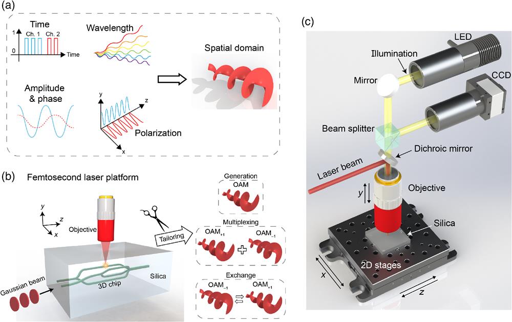
Increasing data transmission capacity is a persistent demand for optical interconnects. Recently, different physical dimensions of light waves, including time,1 amplitude,2 phase,3 wavelength,4 and polarization,5 have been fully utilized to scale the data traffic. Even though various multiplexing techniques exploiting these physical dimensions have been developed, it is becoming rather difficult to follow the demand of a global network that is growing by 40% annually.6 To keep pace with the ever-increasing demand, a new physical dimension of light is urgently needed. Fortunately, space-division multiplexing technology that transmits orthogonal spatial modes loaded with different signals in an optical interconnect system has further improved the transmission capacity, providing a new degree of freedom for capacity scaling of optical interconnects7
![]()
Figure 1.(a) Multiple physical dimensions of light waves: from traditional ones to the spatial domain (e.g., OAM modes). (b) Concept of 3D photonic chips fabricated by FSLW for tailoring spatial modes (OAM generation/multiplexing/exchange). (c) Fabrication setup for FSLW.
Integrated photonic chips with a small footprint, high efficiency, and low cost are emerging with the rapid development of silicon photonics. Remarkably, most optical devices based on silicon photonics, including lasers,14
In this work, we propose and demonstrate FSLW-based 3D photonic chips for orbital angular momentum (OAM) mode-36
Sign up for Advanced Photonics TOC. Get the latest issue of Advanced Photonics delivered right to you!Sign up now
2 Results
2.1 On-Chip OAM Mode Generation
In this work, the first 3D photonic chip for spatial mode tailoring is an on-chip OAM mode generator; its concept and principle are illustrated in Fig. 2(a). The chip is fabricated using the FSLW technique. The detailed fabrication process can be seen in the Appendix. The on-chip OAM mode generator consists of an input waveguide, a Mach–Zehnder interferometer (MZI), and a trench waveguide. The input waveguide and the trench waveguide are designed to support the fundamental and higher-order modes. The principle of the on-chip OAM mode generator is as follows. First, the light launched into the input waveguide excites the fundamental mode. Then the MZI structure (colored by red) that introduces a phase shift in one arm converts the fundamental mode to the first-order quasi-transverse electric mode () (see Note 1 in the Supplementary Material). The generation of the OAM mode is based on the specially designed trench waveguide. The mode can be considered as the in-phase combination of the diagonally and anti-diagonally distributed linearly polarized (LP)-like modes. When the phase difference between these two LP-like modes is or , the OAM mode with a topological charge of or is generated.
![]()
Figure 2.On-chip OAM mode generator. (a) Concept and principle of the trench-based OAM generator. (b) Structure of trench waveguide and its supporting higher-order modes. (c) Simulated LP-like modes and their synthesized OAM modes. (d) Experimental results of OAM generator with different trench locations: (d1) trench facet images captured by an optical microscope, (d2) measured mode profiles, and (d3) measured interferograms (interference with a reference Gaussian beam). Scale bar,
The trench waveguide and its supported eigenmodes are shown in Fig. 2(b). Four parameters define the geometry, which are the waveguide width (), waveguide height (), trench width (), and trench height (). The trench waveguide supports two orthogonal LP-like modes at 1550 nm, which are diagonally and antidiagonally distributed by choosing the proper geometry (see Note 2 in the Supplementary Material). Here, the and are set to 17 and , respectively. and are set to 3 and , respectively. These two LP-like modes are nondegenerate due to the asymmetrical structure. Thus, the mode can simultaneously excite two orthogonal LP-like modes with different propagation constants. Further, as depicted in Fig. 2(c), they can be synthesized to OAM modes with topological charges of and after propagating through different distances, corresponding to phase differences of and , respectively. Except for changing the length of the trench waveguide, one can also swap the sign of the topological charge of OAM modes by altering the trench location.
The experimental results for the OAM generation with different trench locations are shown in Fig. 2(d), where are the facet images of the trench waveguides, output mode profiles, and corresponding interferograms (by interference with a reference Gaussian beam), respectively. These four OAM generators are entirely the same, except for the location of the trench structure. We characterize these OAM modes by retrieving their phase profiles and calculating their OAM spectra (see Note 3 in the Supplementary Material). The OAM phase purities for each case are . The details of phase retrieving and mode purity calculation can be found in the Appendix. The measured mode profiles in Fig. 2(d2) show slight defects in the experiment, which are mainly caused by the slight fabrication error of waveguide structures, i.e. inaccurate phase difference (derivation from ) between the two arms of the MZI as well as inaccurate phase difference (derivation from ) between the two eigenmodes of the trench waveguide. However, they still show a high OAM phase purity over 92%. The mode quality might be improved by further reducing the fabrication error with optimized fabrication parameters, such as the laser power, scanning speed, and scanning spacing.
In the experiment, when the polarization state of the input beam changes, the output OAM mode profile keeps almost unchanged, and the polarization state of the output OAM mode almost remains the same as the input beam. That is because, according to our characterization in the experiment, the birefringence induced by FSLW is estimated to be lower than . Meanwhile, the waveguide structures of the 3D photonic chip are relatively symmetrical and short in length.
2.2 On-Chip OAM Mode (De)Multiplexer and Exchanger
Other typical functions for spatial mode tailoring are mode (de)multiplexing and exchange. We propose an on-chip OAM mode multiplexer based on the variation of the trench waveguide; its concept and principle are illustrated in Fig. 3(a). The OAM mode multiplexer consists of two input waveguides, two MZIs, and a specially designed trench waveguide. The angle between the planes (colored cyan and yellow) where the two MZIs are located is 90 deg. At port 1, the fundamental mode is converted to an LP-like mode with the diagonal distribution by the MZI. Before the trench waveguide, the LP-like mode excites two higher-order and modes equal in phase. Then when the phase difference of these two modes is , the OAM mode with the topological charge of is generated at the output. The same principle is applied to port 2, except for the opposite sign of phase difference () and topological charge number () of the OAM mode.
![]()
Figure 3.On-chip OAM mode multiplexer. (a) Concept and principle of the trench-based OAM mode multiplexer. (b) Structure of the trench waveguide and the supported higher-order eigenmodes (
Figure 3(b) shows the detailed structure of the trench waveguide and the higher-order eigenmodes ( and ) that the waveguide supports. Unlike the former, the trench here is located at the middle top of the waveguide rather than the corners. and are the waveguide width and height, respectively. and are the trench width and height, respectively. By introducing a small trench structure, the degeneracy of and modes is lifted, which means they have different effective refractive indices. The length of the trench waveguide can be expressed by
Simulation results of the OAM mode multiplexer for input from ports 1 and 2 with phase differences of 0, , , , and between and modes in the trench waveguide are depicted in Fig. 3(c). When the phase difference is , the outputs are diagonally and anti-diagonally (anti-diagonally and diagonally) distributed LP-like modes for input from ports 1 and 2. When the phase difference is , the outputs are OAM modes with the topological charge of and ( and ) for input from ports 1 and 2, verified by their phase profiles. Also, it can be seen that the mode exchange happens when the phase difference changes from to .
We experimentally demonstrate the OAM mode multiplexing and exchange in our fabricated 3D photonic chip. Figure 3(d) shows a similar mode evolution with our simulation results in Fig. 3(c). When the trench length is 0 or 5.00 mm, corresponding to the phase difference of 0 or , the mode profiles are diagonally and anti-diagonally distributed LP-like modes for input from ports 1 and 2. When the trench length is 2.50 mm, corresponding to the phase difference of , the mode profiles rotate 90 deg for input from ports 1 and 2, which are anti-diagonally and diagonally distributed LP-like modes. The OAM mode multiplexing happens when the trench length is 1.25 mm. and modes are generated under this condition; this is verified by their interferograms. By extending the trench length to 3.75 mm, OAM modes swap with each other, where is converted to for input from port 1, and is converted to for input from port 2 simultaneously.
Furthermore, we characterize all four OAM modes, retrieving their phase profiles and calculating their OAM spectra (see Note 5 in the Supplementary Material). The OAM phase purities are . The details of phase retrieving and mode purity calculation can be found in the Appendix. Similar to the OAM mode multiplexer, we can also realize the OAM mode demultiplexer simply by using it in an opposite way.
2.3 Chip–Chip Optical Interconnects
Using the designed and fabricated 3D photonic chips for MDM with OAM modes, we demonstrate the chip–chip optical interconnects. The fabricated 3D photonic chips are packaged with single-mode fibers (SMFs) first, as shown in Fig. 4(a). The detailed packaging procedure can be found in Note 6 in the Supplementary Material. The experimental setup for chip–chip optical interconnects is shown in Fig. 4(b). A 1550-nm laser is modulated by an optical I/Q modulator driven by an arbitrary waveform generator (AWG) to generate the 8-ary quadrature amplitude modulation (8-QAM) signal at the transmitter side. A polarization controller (PC) is used to optimize the state of polarization. The amplified optical signal by an erbium-doped fiber amplifier (EDFA) is divided into two channels by an optical coupler (OC), and one of them is transmitted through an additional 1-km SMF for decoherence. Two channel optical signals carried by Gaussian modes are first coupled into an OAM mode multiplexer from inputs 1 and 2, which are transformed into and modes through the 1.25-mm trench waveguide. These two OAM modes are then coupled into an OAM mode demultiplexer with a trench of the same length and are converted back to Gaussian modes at outputs 1 and 2. The output optical signals are amplified by another EDFA on the receiver side. Then a coherent receiver followed by a local oscillator is used to analyze 8-QAM signals for the performance evaluation. Variable optical attenuators (VOAs) and the following EDFAs are used to adjust the received optical signal-to-noise ratio (OSNR). The measured crosstalk matrix for two inputs and two outputs is plotted in Fig. 4(c), which is . The measured bit-error rate (BER) curves for OAM modes transmission are plotted in Fig. 4(d). Compared to the back-to-back case, the measured OSNR penalties at a BER of [7% overhead hard-decision forward-error correction (HD-FEC) threshold] for multiplexing transmission of and modes are less than 1.3 and 3.5 dB, respectively. The insets in Fig. 4(d) are their typical constellations.
![]()
Figure 4.(a) Middle, photo of the packaged on-chip OAM mode multiplexer and demultiplexer. Left, zoom-in view of the OAM mode multiplexer. Right, zoom-in view of the OAM mode demultiplexer. (b) Experimental setup for chip–chip optical interconnects with OAM modes. PC, polarization controller; EDFA, erbium-doped fiber amplifier; AWG, arbitrary waveform generator; OC, optical coupler; SMF, single-mode fiber; and VOA, variable optical attenuator. (c) Measured crosstalk matrix. (d) Measured BER performance and constellations.
2.4 Chip–Fiber–Chip Optical Interconnects
Using the designed and fabricated 3D photonic chips for MDM with OAM modes, we also demonstrate the chip–fiber–chip optical interconnects. Here, we use two individual OAM modes (de)multiplexers interconnected by a 2-km OAM fiber that supports OAM modes. Similarly, the OAM mode (de)multiplexers are packaged first, as shown in Fig. 5(a). The experimental setup for chip–fiber–chip optical interconnects is shown in Fig. 5(b), which is similar to the setup in Fig. 4(b). The difference is that the multiplexed OAM modes are transmitted through an additional 2-km-long OAM fiber. In addition, the transmitted laser is modulated with a quadrature phase-shift keying (QPSK) signal. At the receiver side, the output optical signals are amplified and then a coherent receiver followed by a local oscillator is used to analyze QPSK signals for the performance evaluation. Figure 5(c) shows the measured intensity profiles of the generated mode, mode, and their multiplexing after propagating through the OAM fiber. The measured crosstalk matrix for two inputs and two outputs is plotted in Fig. 5(d), which is . The measured BER curves for OAM multiplexing transmission are plotted in Fig. 5(e). Compared to the back-to-back case, the measured OSNR penalties at a BER of the 7% overhead HD-FEC threshold () for multiplexing transmission of and are less than 4.6 and 5.7 dB, respectively. The insets in Fig. 5(e) are their typical constellations.
![]()
Figure 5.(a) Photos of the packaged on-chip OAM mode multiplexer (left), OAM mode demultiplexer (middle), and unpackaged OAM mode (de)multiplexers (right) in the silica substrate. (b) Experimental setup for chip–fiber–chip optical interconnects with OAM modes. (c) Measured intensity profiles of OAM modes after propagating through the 2-km OAM fiber. (d) Measured crosstalk matrix. (e) Measured BER performance and constellations.
3 Discussion
In summary, we propose and demonstrate a 3D photonic chip platform for versatile spatial mode optical interconnects. Two kinds of 3D photonic chips based on the trench waveguides are designed and fabricated for manipulating the OAM modes, including the OAM mode generation, (de)multiplexing, and exchange. The OAM spectra of the generated OAM modes output from the on-chip multiplexers are analyzed, showing a high mode purity . We also demonstrate chip–chip and chip–fiber–chip optical interconnects with OAM modes using the fabricated 3D photonic chips. OAM modes multiplexing transmission carrying 8-QAM and QPSK signals are successfully demonstrated in the experiment with favorable performance.
Two OAM mode channels are employed in the experiment. There are several potential approaches that might be considered to further increase the number of mode channels. Firstly, reducing the waveguide size and rearranging them in a proper way may provide extra space for more mode channels. Secondly, a photonic lantern structure using special geometrical arrangement might be used for a large number of spatial modes,41 and OAM modes could be obtained by using a complex trench waveguide structure. Thirdly, a free propagation region employing a Rowland circle might be used, and circular patterned apertures of 3D structures could sample and retrieve spatially overlapped multiple OAM modes.32
In the designed and fabricated 3D photonic chip, the bending radii of the bend waveguides are large enough (over 30 mm radius) with negligible bending loss. The propagation loss of single-mode waveguides is about 1 dB/cm. The extra loss caused by the beam splitting and combining is about 0.5 dB. The propagation loss of the trench waveguide is about 1.5 dB/cm. The coupling loss between the waveguide and fiber after packaging is about 1 dB/facet. The overall insertion loss of the OAM mode multiplexer is less than 5 dB. With future improvement, the propagation loss and extra loss might be reduced by optimizing the structure design and fabrication parameters. Moreover, the coupling loss might be reduced by matching the mode fields between the 3D photonic chip and fiber.
This work demonstrates a compact, multi-functional and flexible platform for tailoring the spatial structure of lightwaves and enabling chip-assisted spatial mode optical interconnects. The 3D photonic chips fabricated by the FSLW technique may find more and more exciting applications with spatial modes.
4 Appendix: Methods
4.1 3D FSLW Technique
The 3D FSLW technique is based on the laser-induced refractive index change in transparent materials. When a femtosecond laser beam is ultrafocused inside the glass, nonlinear absorption occurs. Under the proper conditions (the pulse duration, pulse energy, and focusing numerical aperture), it will produce a localized refractive index change in the focal volume, which can reach the submicrometer scale.42
The setup for FSLW is depicted in Fig. 1(c). A well-polished silica substrate is mounted on the 2D stages (Aerotech), linearly moving along the and directions. A femtosecond laser beam reflected by a dichroic mirror propagates through an objective. The objective translating along the direction controls the depth of the foci in the substrate during fabrication. In addition, an LED illumination propagates through a mirror, beam splitter, dichroic mirror, objective, and lightens the fabricated sample. The sample image is then reflected through the objective, dichroic mirror, beam splitter, and finally captured by a CCD. In this way, we can achieve real-time observation of fabrication. According to the tracks we program, arbitrary structures can be processed.
A femtosecond laser (PHAROS, 200 kHz repetition rate, 515 nm wavelength, and 340 fs pulse width) is focused by a 0.42 NA objective (Mitutoyo long working distance objective) at 0.2 mm below the surface of silica. The cross section of foci perpendicular to the scanning direction ( direction) is elliptical. Therefore, a mechanical slit (along the direction) is mounted before the objective.43,44 By adjusting the width of the slit, the Gaussian beam becomes elliptical with an ellipticity of 0.19 (defined by the ratio of the major axis and minor axis). The desired foci with a symmetric cross section can be produced. In the experiment, the pulse energy before the objective with a slit is 355 nJ. The multiscan technique is used with a scanning speed of . The scanning spacing is in the direction and in the direction (considering the refractive index). The refractive index contrast is estimated to be about to . Additionally, the birefringence is estimated to be lower than .
4.2 Phase Retrieving and Mode Purity Calculation
We use the off-axis digital holography technology45,46 to reconstruct the wavefront of generated OAM beams for mode purity characterization. Off-axis digital holography allows a single-exposure acquisition of a beam wavefront by introducing a slight angle between the generated OAM beam and reference beam as they interfere at the digital camera plane. An off-axis hologram containing linear interference fringes is recorded in the experiment. We utilize a two-dimensional Fourier transform to separate the autocorrelation terms and cross-correlation terms of these linear interference fringes in the spatial-frequency domain. Since the cross-correlation terms act as a carrier for the wavefront of the OAM beam, one can retrieve the wavefront of the OAM beam by applying inverse Fourier transform to separated cross-correlation terms. Then the mode purity of the generated OAM beam can be calculated as the normalized power weight coefficient47 using
Jian Wang received his PhD in physical electronics from Wuhan National Laboratory for Optoelectronics, Huazhong University of Science and Technology, China, in 2008. He worked as a postdoctoral research associate in Optical Communications Laboratory at the University of Southern California, United States, from 2009 to 2011. Currently, he is working as a professor at Wuhan National Laboratory for Optoelectronics, Huazhong University of Science and Technology, China. He is vice director of Wuhan National Laboratory for Optoelectronics, Huazhong University of Science and Technology, China. He was elected as an OPTICA fellow (formerly OSA fellow) in 2020 and an SPIE fellow in 2022. He leads the Multi-dimensional Photonics Laboratory. His research interests include optical communications, optical signal processing, silicon photonics, photonic integration, orbital angular momentum, and structured light.
Biographies of the other authors are not available.
References
[6] D. J. Richardson. Filling the light pipe. Science, 330, 327-328(2010).
[10] G. Labroille et al. Mode selective 10-mode multiplexer based on multi-plane light conversion, Th3E.5(2016).
[11] S. Bade et al. Fabrication and characterization of a mode-selective 45-mode spatial multiplexer based on multi-plane light conversion, Th4B.3(2018).
[15] Q. Bao et al. On-chip single-mode CdS nanowire laser. Light Sci. Appl., 9, 42(2020).
[33] P. Mitchell et al. 57 channel (19×3) spatial multiplexer fabricated using direct laser inscription, M3K.5(2014).
[35] S. Gross et al. Ultrafast laser-written sub-components for space division multiplexing, W1A.1(2020).
[36] S. Ramachandran, P. Kristensen. Optical vortices in fiber. Nanophotonics, 2, 455-474(2013).
[39] X. Wang et al. Recent advances on optical vortex generation. Nanophotonics, 7, 1533-1556(2018).
[42] E. Mazur. Femtosecond laser micromachining in transparent materials, BWB4(2010).
[46] M. Mazur et al. Characterization of long multi-mode fiber links using digital holography, W4C.5(2019).

Set citation alerts for the article
Please enter your email address
© Copyright 2018-2021 | Chinese Laser Press. All Rights Reserved 沪ICP备15018463号-20