• Photonics Research
  • Vol. 10, Issue 10, 2422 (2022)
Ranjan Das1、†,*, Yanran Xie1、†, Henry Frankis1, Keru Chen1, Hermann Rufenacht2, Guillaume Lamontagne2, Jonathan D. B. Bradley1, and Andrew P. Knights1
Author Affiliations
  • 1Department of Engineering Physics, McMaster University, Hamilton, Ontario L8S 4L7, Canada
  • 2McDonald Detwiler Associates, Sainte-Anne-de-Bellevue, Quebec H9X 3R2, Canada
  • show less
    DOI: 10.1364/PRJ.463832 Cite this Article Set citation alerts
    Ranjan Das, Yanran Xie, Henry Frankis, Keru Chen, Hermann Rufenacht, Guillaume Lamontagne, Jonathan D. B. Bradley, Andrew P. Knights. Gain-enabled optical delay readout unit using CMOS-compatible avalanche photodetectors[J]. Photonics Research, 2022, 10(10): 2422 Copy Citation Text show less
    (a) Schematic of the on-chip group delay measurement system using low-bandwidth electronics. RF modulated optical signal experiences ring delay and subsequently, is detected and measured by PD and VNA, respectively. (b) RF phase-to-delay transformation illustration. CW, continuous-wave; EO modulator, electro-optic modulator; PC, polarization controller; Ring, ring resonator; PD, photodetector; RF Amp., RF amplifier; EVNA, electrical vector network analyzer; ∠ϕ21, phase response of S21; τ(λ), delay, and (ϕ21T−ϕ21S), phase shift due to the MRR only.
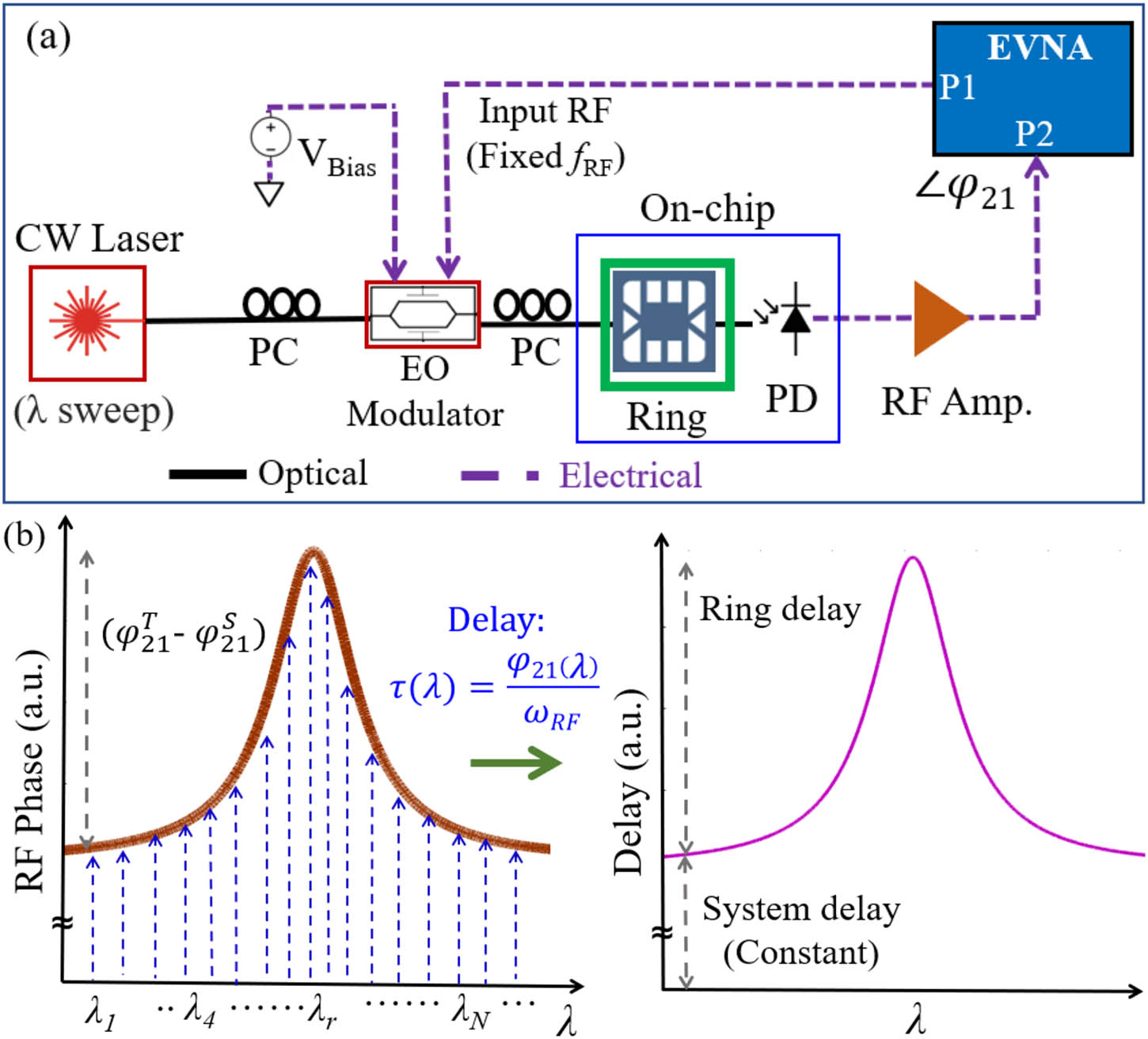
    Fig. 1. (a) Schematic of the on-chip group delay measurement system using low-bandwidth electronics. RF modulated optical signal experiences ring delay and subsequently, is detected and measured by PD and VNA, respectively. (b) RF phase-to-delay transformation illustration. CW, continuous-wave; EO modulator, electro-optic modulator; PC, polarization controller; Ring, ring resonator; PD, photodetector; RF Amp., RF amplifier; EVNA, electrical vector network analyzer; ϕ21, phase response of S21; τ(λ), delay, and (ϕ21Tϕ21S), phase shift due to the MRR only.
    Measured MRR characteristics. (a) Prototype of the fabricated MRR; (b) ring resonance tuning by adjusting integrated heater power supply.
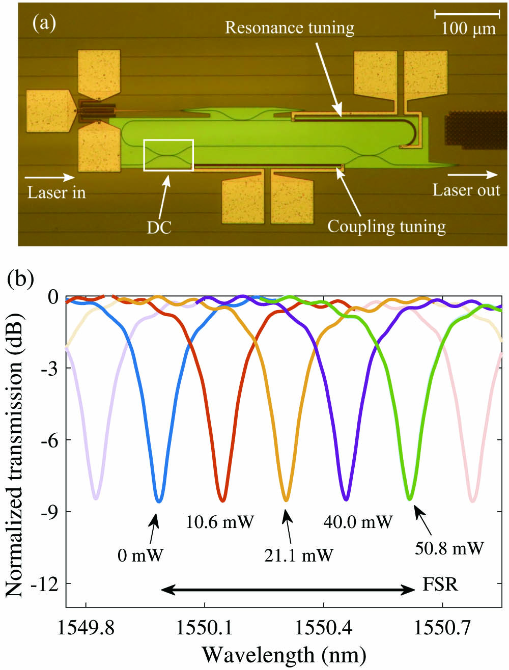
    Fig. 2. Measured MRR characteristics. (a) Prototype of the fabricated MRR; (b) ring resonance tuning by adjusting integrated heater power supply.
    Measured MRR characteristics. (a) Ring coupling k tuning by integrated heater and (b) ring–bus coupling (k) variation for different heater powers.
    Fig. 3. Measured MRR characteristics. (a) Ring coupling k tuning by integrated heater and (b) ring–bus coupling (k) variation for different heater powers.
    Cross-sectional view of the (a) Si APD, (b) Ge SACM APD, and (c) Ge PIN PD, respectively. Light enters these waveguide PDs normal to the plane of the page.
    Fig. 4. Cross-sectional view of the (a) Si APD, (b) Ge SACM APD, and (c) Ge PIN PD, respectively. Light enters these waveguide PDs normal to the plane of the page.
    Characterization of the avalanche PDs. (a), (d) Si and Ge APD photocurrent versus bias; (b), (e) photocurrent versus optical power; and (c), (f) small-signal bandwidth of the Si APD and Ge SACM APD for different bias configurations. Popt indicates input optical power at fiber tip.
    Fig. 5. Characterization of the avalanche PDs. (a), (d) Si and Ge APD photocurrent versus bias; (b), (e) photocurrent versus optical power; and (c), (f) small-signal bandwidth of the Si APD and Ge SACM APD for different bias configurations. Popt indicates input optical power at fiber tip.
    Characterization of Ge PIN PD. (a) Ge PD I-V response operating at PIN mode, and (b) small-signal response of the Ge PIN detector under different reverse bias voltages. Popt represents input optical power at fiber tip.
    Fig. 6. Characterization of Ge PIN PD. (a) Ge PD I-V response operating at PIN mode, and (b) small-signal response of the Ge PIN detector under different reverse bias voltages. Popt represents input optical power at fiber tip.
    Measured RF phase and delay responses (after compensating for static components) using (a) Si APD, (b) Ge SACM APD, and (c) Ge PIN PDs for different ring–bus coupling configurations, respectively.
    Fig. 7. Measured RF phase and delay responses (after compensating for static components) using (a) Si APD, (b) Ge SACM APD, and (c) Ge PIN PDs for different ring–bus coupling configurations, respectively.
    Comparison of measured delay results with simulations for (a) Si APD (k=0.62) and (b) Ge SACM APD (k=0.73) PD. Black represents simulation, whereas orange and blue are for measured results.
    Fig. 8. Comparison of measured delay results with simulations for (a) Si APD (k=0.62) and (b) Ge SACM APD (k=0.73) PD. Black represents simulation, whereas orange and blue are for measured results.
    Measured delay responses for a constant ring–bus coupling using (a) Si APD and (b) Ge SACM APD PDs with different bias voltages.
    Fig. 9. Measured delay responses for a constant ring–bus coupling using (a) Si APD and (b) Ge SACM APD PDs with different bias voltages.
    Minimum required optical power measurement for different bias voltages of the Si APD.
    Fig. 10. Minimum required optical power measurement for different bias voltages of the Si APD.
    RF signal phase responses for different input optical powers to the (a) Si APD and (b) Ge SACM APD.
    Fig. 11. RF signal phase responses for different input optical powers to the (a) Si APD and (b) Ge SACM APD.
    (a) RF spectra for different integrated PDs and (b) broader frequency range for harmonic analysis. The inset shows zoomed-in view of the RF signals far away from the fundamental component.
    Fig. 12. (a) RF spectra for different integrated PDs and (b) broader frequency range for harmonic analysis. The inset shows zoomed-in view of the RF signals far away from the fundamental component.
    Measurement MethodDelay Element and DetectorErrorResolutionOn-Chip RF AmplificationRemarksReference
    Optical vector analyzerSi waveguide spiral (6.56 cm long) with maximum delay range of 0–320 ps, detector not on-chip<0.5%<1  psNoHigh accuracy, expensive infrastructure[34]
    Optical vector analyzerCascaded Si MRR (600  μm×300  μm) with maximum tunable delay range of 0–1700 ps, detector not on-chip<0.5%<1  psNoHigh accuracy, expensive infrastructure[35]
    Optical time-domain reflectometryExternal single-mode fibers with differential delay of 0.4 ps, detector type not mentioned>12%N.A.NoRequiring high power optical pulses[36]
    Optical frequency-domain reflectometryFiber Bragg grating with maximum tunable delay range of 0–253 ns, external detector25%15 psNoRequiring complex signal processing[39]
    Frequency-shifted self-heterodyneSingle-mode fiber with maximum delay range of 50.13 ns, external detectorN.A.N.A.NoRequiring narrow linewidth laser source[44]
    VNASingle Si MRR (500  μm×100  μm) with tunable delay range of 0–300 ps, integrated on-chip detectors<2%<10  ps10 dBbLow BW electronics without RF amplifiers TLS, Max. optical power: −2 dBmThis work
    Table 1. Comparison of Different Delay Measurement Approachesa
    Ranjan Das, Yanran Xie, Henry Frankis, Keru Chen, Hermann Rufenacht, Guillaume Lamontagne, Jonathan D. B. Bradley, Andrew P. Knights. Gain-enabled optical delay readout unit using CMOS-compatible avalanche photodetectors[J]. Photonics Research, 2022, 10(10): 2422
    Download Citation