Ranjan Das1,†,*, Yanran Xie1,†, Henry Frankis1..., Keru Chen1, Hermann Rufenacht2, Guillaume Lamontagne2, Jonathan D. B. Bradley1 and Andrew P. Knights1|Show fewer author(s)
Ranjan Das, Yanran Xie, Henry Frankis, Keru Chen, Hermann Rufenacht, Guillaume Lamontagne, Jonathan D. B. Bradley, Andrew P. Knights, "Gain-enabled optical delay readout unit using CMOS-compatible avalanche photodetectors," Photonics Res. 10, 2422 (2022)
Copy Citation Text
A compact time delay unit is fundamental to integrated photonic circuits with applications in, for example, optical beam-forming networks, photonic equalization, and finite and infinite impulse response optical filtering. In this paper, we report a novel gain-enabled delay readout system using a tunable optical carrier, low-frequency RF signal and CMOS-compatible photodetectors, suitable for silicon photonic integration. The characterization method relies on direct phase measurement of an input RF signal and thereafter extraction of the delay profile. Both integrated silicon and germanium photodetectors coupled with low-bandwidth electronics are used to characterize a microring resonator-based, true-time delay unit under distinct ring–bus coupling formats. The detectors, used in both linear and avalanche mode, are shown to be successful as optical-to-electrical converters and RF amplifiers without introducing significant phase distortion. For a Si–Ge separate-absorption-charge-multiplication avalanche detector, an RF amplification of 10 dB is observed relative to a Ge PIN linear detector. An all-silicon defect-mediated avalanche photodetector is shown to have a 3 dB RF amplification compared to the same PIN detector. All ring delay measurement results are validated by full-wave simulation. Additionally, the impact of photodetector biasing and system linearity is analyzed.
1. INTRODUCTION
Over the past few decades, high-density photonic integrated circuits (PICs) with complex features have become increasingly important for communications, computation, and sensing applications [1–4]. Many promising features such as low cost, high yield, small form-factor, high bandwidth, low power, and large volume scalability [5,6] make them attractive for established and emerging areas from photonic hardware accelerators to quantum computing [7–9]. Leveraging the mature complementary metal-oxide-semiconductor (CMOS) processing technology, it is now possible to design a fully monolithic electronic photonic circuit (EPIC) with onboard complex control tuning architectures [10,11]. Silicon (Si) enabling material for CMOS technology, offers the most prominent platform for densely integrated PICs, namely, the Si-on-insulator (SOI) platform. It shapes passive Si photonic integration ideal for reconfigurable or tunable optics where a particular circuit state is tuned to optimally execute a specific task with a limited power budget and footprint while allowing for dense integration of individual elements. Most multifunctional PICs are enabled either by using an asymmetric interferometric design [12,13] or by introducing variable delay blocks [14,15]. In fact, a tunable delay element is the backbone of many integrated photonic circuits, such as optical beam-forming networks (OBFNs), photonic equalizers, reservoir computing, and tunable filter banks [16–21]. For instance, a true-time delay (TTD)-based squint-free photonic beam former is a commonly deployed architecture for a multi-input-multi-output (MIMO) antenna array system [22–25]. In addition, delay dispersive designs are useful for real-time white-space sensing [26–28], a fundamental basis of dynamic spectrum allocation in 5G technology [29].
Static waveguide spirals, dynamic thermal phase-shifter-embedded waveguides, and ring resonators are frequently used as a tunable delay element in PICs. A versatile microring resonator (MRR) that partially confines light by total internal reflection outperforms other technologies in terms of size, wavelength selectivity, tunability, and resonance enhancement [30,31]. Nonetheless, precise optical delay measurement and its proper tuning remain a crucial challenge to any reconfigurable PIC. For example, in a wavelength-division multiplexing (WDM) system, the optical time delay is closely correlated with the bit error rate (BER) and in the case of an OBFN, the beam steering angle [32,33].
In this work, we propose a delay readout circuit enabled by CMOS-compatible photodetectors (PDs) on a standard (SOI) platform. Here the term “delay readout” refers to the precise group delay measurement of an optical delay element. The proposed method is applicable to any type of optical delay unit such as nonresonant, static (spirals or straight or bend waveguides), or dispersive (MRR). We introduce a novel characterization technique employing a tunable continuous-wave (CW) laser source, modulated by a fixed low-frequency RF signal. Optical carrier wavelength () is swept across the region of interest, covering at least one resonance peak to measure the RF signal phase shift; subsequently, the ring delay is extracted using a unique phase-to-delay transformation. We choose an MRR as a variable delay unit for this demonstration; however, the same readout circuit can be engaged to characterize any other delay cell. The major contribution of this work includes: (i) demonstration, for the first time, to the best of our knowledge, of an accurate delay measuring circuit using gain-assisted integrated avalanche PDs. In the case of a Ge–Si separate-absorption-charge-multiplication (SACM) avalanche photodiode (APD), an on-chip RF gain of 10 dB is achieved as compared to the use of PIN Ge detectors. We thus illustrate that gain mode avalanche PDs are well-positioned for this application, providing concurrent optoelectric conversion and RF amplification without inserting catastrophic phase distortion or higher-order harmonics into the system; (ii) photocurrent linearity, responsivity, and small-signal behavior of the integrated detectors are thoroughly analyzed, and operation boundaries for the specific detector design are reported; (iii) defect-mediated Si-APD and conventional Ge PIN detectors are also examined to demonstrate the robustness of the delay measuring unit; (iv) a detailed discussion on the detector bias settings, minimum optical power, and system linearity is presented; (v) delay is measured for distinct ring–bus coupling configurations and is subsequently verified by full-wave simulation results; and (vi) low-bandwidth electronics with an electrical vector network analyzer (VNA) are used to illustrate the measurement concept successfully.
Sign up for Photonics Research TOC. Get the latest issue of Photonics Research delivered right to you!Sign up now
This paper is organized as follows. Section 2 provides the delay measurement principle and overall system architecture. Section 3 discusses the characterization of the integrated devices: MRR, Si APD, and Ge (SACM APD and PIN) PDs. Section 4 provides delay measurement results for three different ring–bus coupling conditions with monolithic PDs. It also compares measured delay results with simulation. A discussion on the detector bias voltage conditions, linearity response, and measurement accuracy is provided in Section 5. Finally, Section 6 provides a succinct conclusion to our work.
2. DELAY MEASUREMENT PRINCIPLE
Several techniques have been used previously to measure group delay, each with advantages or disadvantages in terms of capital cost, complexity, and accuracy. For example, an optical vector network analyzer (OVNA) has been employed to measure group delay of spirals and ring resonator-based variable delay elements [34,35]. However, OVNA units can be prohibitively expensive for many academic research environments. Other methods including optical time-domain reflectometry (OTDR) [36,37] and optical frequency-domain reflectometry (OFDR) [38,39] have been applied. OTDR works by monitoring the propagation delay of a backscattered signal, but suffers from poor temporal resolution, suitable thus only for low-resolution applications. OFDR provides better time resolution where time domain information is processed using fast Fourier transform (FFT) with digital signal processors. Nonetheless, at microwave- or millimeter-wave frequencies, digital processing is limited due to excessive memory requirement, power consumption, and costly analog-to-digital conversion [40]. In Ref. [41], optical low-coherence reflectometry (OLCR) was used for delay estimation, but the resolution was limited by the optical path. Time-delay measurement of photonic components by sweeping the electrical frequency from a VNA has been reported [42,43]. Although this technique has better accuracy, it requires high-speed electronics and complex postprocessing for phase de-embedding. A frequency-shifted self-heterodyning approach was explored in Ref. [44], in which an additional frequency shifter was deployed to measure optical time delay. Also, an innovative off-chip delay measuring technique with a fixed RF signal was reported in Ref. [45]. In another work, a discrete optical delay measurement setup with amplitude modulation was proposed to achieve subpicosecond delay measurement uncertainty [46]. The monolithic implementation of a real-time optical delay measuring circuit for a dispersive or nonresonant delay block and thence tuning of a large photonic integrated system remains an open research problem in integrated photonics and leads us to propose a new delay measuring method.
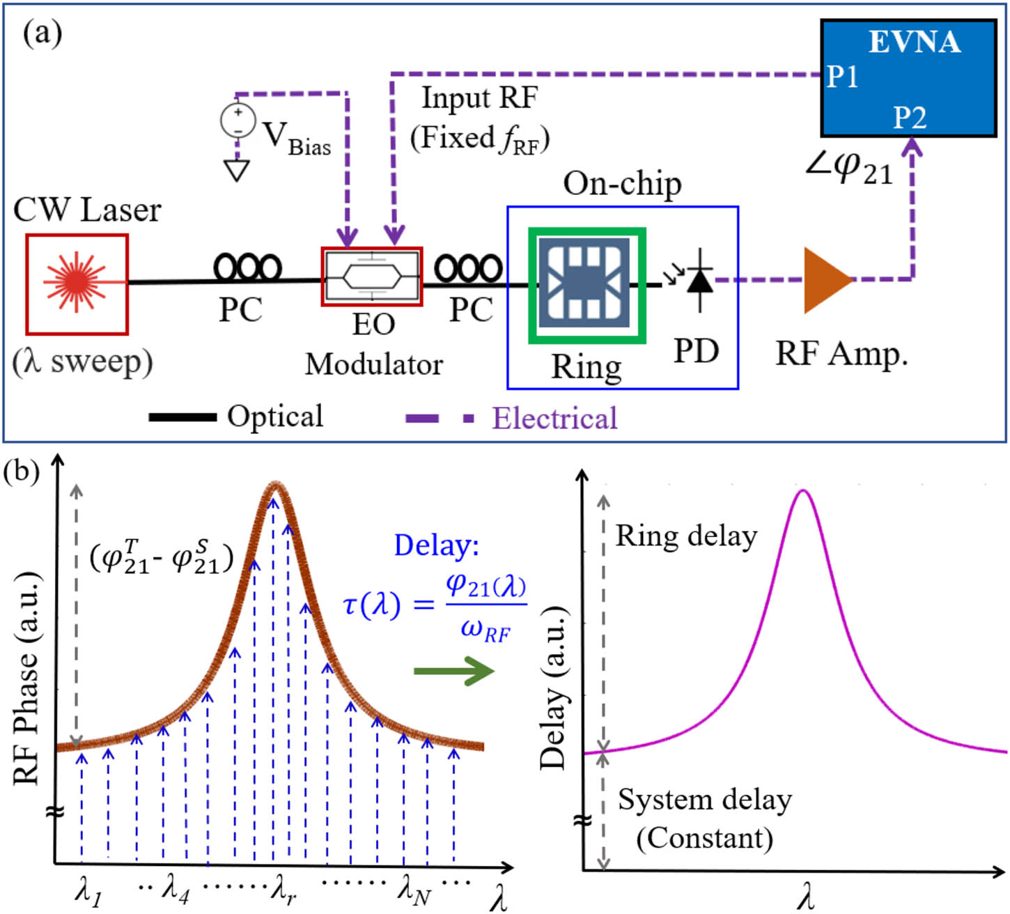
When an RF-modulated optical signal is passed through a delay structure such as a ring resonator, it experiences a phase shift which, in the case of ring resonators, depends on the overall ring–bus coupling coefficient. Also, the RF signal phase shift is maximum at the resonance point and decreases as the carrier wavelength deviates from the resonance point at off-resonance wavelengths, i.e., exhibiting a dispersive delay profile [21]. Thus, a wavelength-variant phase profile can be observed when an optical carrier is probed for different discrete wavelengths covering one or a multiple of free-spectral ranges (FSRs) of the ring with a fixed frequency RF signal. One may thus employ a low-frequency RF signal to measure the phase shift, which removes the reliance on high-speed electronics (unlike the electrical frequency sweep approach [42]). Such a carrier wavelength-dependent RF phase change enables us to extract a precise delay distribution using a unique phase-to-delay mapping. The overall measurement system with phase-to-delay transformation is depicted in Fig. 1.
Figure 1.(a) Schematic of the on-chip group delay measurement system using low-bandwidth electronics. RF modulated optical signal experiences ring delay and subsequently, is detected and measured by PD and VNA, respectively. (b) RF phase-to-delay transformation illustration. CW, continuous-wave; EO modulator, electro-optic modulator; PC, polarization controller; Ring, ring resonator; PD, photodetector; RF Amp., RF amplifier; EVNA, electrical vector network analyzer; , phase response of ; , delay, and (), phase shift due to the MRR only.
The system setup includes a tunable laser source, optical modulator, MRR (as a variable delay unit), and PD, as shown in Fig. 1(a). An RF signal (with fixed frequency ) from an electrical VNA experiences a relative phase change due to the microring as a function of coupling and carrier wavelength and subsequently is monitored by the PD, which is connected to a second port of the same VNA. A relative phase shift (with respect to input) can directly be measured from the VNA and multiple phase measurements at different optical wavelengths cover the desired carrier spectral range. The number of such discrete measured points will determine the accuracy of the delay measurement and can be adapted according to error tolerance. Subsequently, total delay can be derived from measured phase responses as [47] where represents measured RF phase shift w.r.t. input signal phase; and are input RF signal frequency (rad/s) and delay response, respectively. In practice, can be obtained by measuring the phase of the signal from a two-port VNA instrument [48]. Note that one should be able to obtain total delay using Eq. (1). Total system delay, for instance, can be extracted precisely after measuring RF signal phase response at off-resonance wavelengths. This will be further discussed in Section 4.
Note that a measured RF phase shift includes total delay due to the MRR plus the system delay (from various components, RF cables, and fibers). System delay is constant, whereas ring delay varies with input optical excitation wavelength (), as illustrated in Fig. 1(b). One can de-embed static delay components to determine dynamic ring delay () as where represents the measured RF phase shift at off-resonance wavelengths, which essentially indicates static system delay. Generally, system delay is in the order of a few nanoseconds (mostly due to RF connecting cables), whereas maximum ring delay is limited to a few hundreds of picoseconds, depending on the ring–bus coupling coefficient (). Nevertheless, the proposed approach is suitable for measuring the delay profile of nonresonant devices such as waveguides and spirals. Furthermore, the proposed readout circuit is wavelength-independent, and delay can be measured at any optical wavelength with a suitable PD.
3. DEVICE CHARACTERIZATION
The relative delay response of an optical ring resonator is demonstrated using a Mach–Zehnder interferometer (MZI)-assisted ring resonator [22] and three types of CMOS-compatible PDs: (i) defect-mediated Si APD [49], (ii) germanium–silicon (Ge–Si) APD [50], and (iii) Ge PIN detector [51]. All devices were fabricated at Advanced Micro Foundry (AMF) with their Si photonics multiproject wafer (MPW) fabrication process. Across all designs, the waveguide core layer consists of 220-nm-thick Si on a 2-μm-thick buried oxide (BOX) layer. The slab waveguides are defined with a 130 nm etch of the Si layer, leaving a 90-nm-thick Si slab. Multiple levels of boron (-type) and phosphorus (-type) doping are achieved with ion implantation and subsequent activation. The process also includes a titanium nitride (TiN) heater layer. Electrical connections to the device and the heater are achieved with multiple aluminum metal layers. The entire structure is encapsulated in 2-μm-thick Si oxide () as a passivation layer. More details of this technology can be found in Ref. [11].
A. Si MRR
MRRs are fundamental building blocks of many complex optical networks. Here we demonstrate an MZI-based MRR [Fig. 2(a)] that features a tunable phase shifter on one of the MZI arms that adjusts the coupling ratio and a second phase shifter within the ring for resonance tuning. The phase shifters are TiN-resistive heaters that modify the phase by changing the refractive index of the Si waveguide via thermo-optic effect. The length of both thermal phase shifters is 230 μm. Light is coupled evanescently into the ring with two directional couplers (DCs) designed for 50/50 coupling. The coupling gap of each of the DCs is 200 nm. The drop port of the MRR couples 10% optical power into a Ge waveguide PD, which is not explored in this study. The bus waveguide tapers from a width of 500 to 170 nm at the edge of the chip to allow for efficient coupling to the input/output fibers. The width of the waveguide defining the ring is 500 nm, and the cavity length of the ring is 995 μm. A similar MZI-embedded MRR was introduced as a TTD element in an OBFN by Meijerink et al. [22].
Figure 2.Measured MRR characteristics. (a) Prototype of the fabricated MRR; (b) ring resonance tuning by adjusting integrated heater power supply.
The tuning of the resonant frequency of the MZI-based MRR is first demonstrated by applying various electrical powers in the phase shifter within the MRR cavity [Fig. 2(b)]. The resonance of the ring can be adjusted freely within the FSR of the MRR, which is determined to be 0.63 nm (78.8 GHz). It is observed that for resonance tuning of an entire order, heater power of 50.8 mW is required. The electrical power needed for a -phase shift for this configuration is thus . Different coupling states are achieved by applying various electrical powers to the microheater on one of the MZI arms. The results are presented in Fig. 3(a). Several transmission spectra (not shown) of the MRR are fitted to find the overall power coupling coefficient [52]. Figure 3(b) illustrates the comparison between the measured data and simulation results [53], which shows excellent agreement. The extracted critical coupling coefficient () is approximately 0.30. It is noted that due to variations in the fabrication process, the 50/50 DCs deviate from the intended design, which results in the coupling coefficient being limited to below a maximum of 0.8 in this work.
Figure 3.Measured MRR characteristics. (a) Ring coupling tuning by integrated heater and (b) ring–bus coupling () variation for different heater powers.
The integrated delay measurement is first demonstrated with a defect-mediated Si APD at the output of the previously described MZI-based MRR. Although Si is transparent at 1550 nm, the intentional inclusion of defects in the waveguide region of the detector introduces subbandgap energy states, which facilitate the absorption of light at this wavelength. Such detectors offer a truly monolithic solution for photodetection and have significant advantages compared to hybrid solutions in terms of fabrication simplicity. The Si APD consists of an integrated π type structure across a 1-μm wide Si waveguide, with 90 nm slabs supporting the and doped regions. The heavily doped regions are separated by 1.6 μm, while the background -doping of the waveguide is approximately , defining the detector as a π device. An oxide etch leaves a 2 μm wide window exposing the underlying Si waveguide, which facilitates the masked implantation of defects through an inert implantation process, specifically ions to a dose of . This is followed by a 5 min 200°C annealing. The length of the active region is 750 μm. Since it is a waveguide type PD, light enters from the passive Si waveguide into the active region, while absorption occurs along the volume of the implanted waveguide. Electrical contact with the - and -doped regions is achieved with aluminum vias and surface contact pads. Similarly, designed structures have been described in detail, for example in Refs. [49,54], and the detailed processes of the technology can be found in Ref. [11]. A schematic cross section is shown in Fig. 4(a).
Figure 4.Cross-sectional view of the (a) Si APD, (b) Ge SACM APD, and (c) Ge PIN PD, respectively. Light enters these waveguide PDs normal to the plane of the page.
The characteristics of the Si APD are shown in Fig. 5(a) for input optical power of at the input fiber tip at a wavelength of 1550 nm. The onset of the avalanche is determined from electric field simulations (not shown), whereby the maximum field value at half the height of the Si slab reaches the impact ionization threshold () for avalanche in Si [55,56]. This also coincides with almost complete depletion of the waveguide. In our designs, the avalanche is approximately 12 V (reverse-biased). The dark current remains below 20 μA at 25 V (reverse-biased). Accounting for an estimated fiber coupling loss of 1.5 dB and an additional loss of 1 dB in the waveguide before the light enters the APD region, the internal responsivity of the Si APD at 25 V is estimated to be . Pertinent to our measurement integrity is the linearity of the APD response. We measured the APD photocurrent as a function of input optical power up to 5 dBm, under various reverse bias conditions [Fig. 5(b)]. The device is shown to be linear under all biases that cover both nonavalanche and avalanche regions. In the integrated measurement of MRR-induced delay, the maximum input power is less than , well within the limit of the APD linear operation. The small-signal RF response of the Si APD was measured with a VNA. The electrical bandwidth of the APD was determined to be more than 10 GHz for all bias voltages. The device bandwidth is limited by carrier transit time at low reverse bias and by the bandwidth gain product at higher reverse bias [49]. However, this small signal bandwidth is fully adequate for the MRR delay measurement. It is important to note the increase in RF power as bias voltage increases, which demonstrates the ability of utilizing a single APD as both an optoelectronic converter and a variable RF power amplifier/attenuator, depending on the bias voltage applied to the device. In this case, an RF power increase of was observed for the APD operating at 20 V compared to 10 V.
Figure 5.Characterization of the avalanche PDs. (a), (d) Si and Ge APD photocurrent versus bias; (b), (e) photocurrent versus optical power; and (c), (f) small-signal bandwidth of the Si APD and Ge SACM APD for different bias configurations. indicates input optical power at fiber tip.
Ge is widely used as the detector material for a Si photonics platform due to its higher absorption in the C-band and ability for integration with Si through direct epitaxy. In this study, we examined two different Ge detector structures: an SACM APD and a PIN.
The Ge-Si SACM APD features a conventional SACM structure, which includes a 500 nm Si multiplication layer, a p-doped field spreading charge layer, and the Ge absorption layer. A schematic cross section of the active detector region is depicted in Fig. 4(b). Light enters from the passive Si waveguide and is then evanescently coupled into the active device region. The details of the detector designs and operating principles can be found in Ref. [57], and we note that the design builds upon the device described in Ref. [50].
Figure 5(d) shows the response of the Ge SACM APD with incident optical power of at the input fiber tip. The gain is obtained from the primary photoresponsivity of the Ge PIN device (described in the next subsection), fabricated on the same wafer as the Ge SACM APD, in conformity with the method described in Refs. [50,57]. The responsivity is estimated to be 2.7 A/W at 20 V reverse bias. The dark current remains less than 1 μA at 20 V. The device shows linear response up to 5 dBm of input optical power [Fig. 5(e)] under various bias conditions. The small-signal bandwidth of the APD is shown in Fig. 5(f), where a bandwidth of is observed for higher reverse biases of 17 and 20 V. The RF signal level is similarly greatly improved with the detector operating in avalanche mode, with a gain of after the bias is increased from 12 to 20 V.
The PIN detector consists of a diode vertically formed across the Si waveguide and i-Ge epitaxially and selectively grown on top of the waveguide. These detectors are offered routinely through the AMF process and have been described often, for example, Ref. [51]. A schematic cross section is presented in Fig. 4(c). The properties of the PIN detector are characterized in Fig. 6. The photocurrent is relatively constant up to a reverse bias of 6 V, with dark current a few tens of nA. The device has a bandwidth of more than 12 GHz and the observed roll-off beyond 12 GHz is likely due to the upper frequency limit (13.5 GHz) of the measurement instrument. Also, the observed RF power differences (w.r.t. bias voltages) are due to the minor variation of the incident optical power to the detector.
Figure 6.Characterization of Ge PIN PD. (a) Ge PD response operating at PIN mode, and (b) small-signal response of the Ge PIN detector under different reverse bias voltages. represents input optical power at fiber tip.
The relative delay of the MZI integrated MRR was demonstrated with the measurement setup, as illustrated in Fig. 1(a). Continuous light was generated by a tunable laser (Agilent 8164B), and then passed through a series of polarization controlling paddles before entering the optical modulator (Fujitsu FTM7937EZ/202). The modulator was biased at the quadrature voltage and was driven by a 100 MHz RF signal from the output port (port-1) of the VNA (Hewlett-Packard 8719C). The bandwidth of the optical modulator is more than 35 GHz, and the VNA is rated for 50 MHz–13.5 GHz operation. Alternatively, a low-bandwidth external optical modulator could also be used for this application. The modulated light was coupled from a lensed fiber into the input waveguide of the on-chip MRR after its polarization was corrected by another set of polarization paddles. The output light from the MRR was then coupled into one of the three types of PD. A high-speed Cascade Infinity RF probe () offered low-impedance electrical contact for the detectors. A Picosecond Pulse Lab 5550B bias tee was used to apply reverse bias to and extract electrical signal from the detectors simultaneously. The electrical RF signal was subsequently amplified with an SHF 100 BP broadband amplifier (30 kHz–25 GHz) before being fed into port-2 of the same VNA. The phase reading of the RF signal was continuously recorded while the input light wavelength was being varied. All off-chip optical connections were provided by single-mode fibers with all electrical elements connected using coaxial cables with SubMiniature version A (SMA) connectors rated for operation. A thermoelectric cooler (TEC, ILX Lightwave LDC-3742) was installed to the stage hosting the PIC to maintain a constant temperature of 20°C for all measurements. The results obtained using the different detectors are presented in the following subsections.
A. Monolithic Si APD
As a first attempt to demonstrate the measurement principle, the Si APD was coupled to the output of the MRR. The RF phase shifts were measured using the VNA, and thereafter delay responses were extracted according to Eq. (2). The measured phase shifts and delay responses are plotted in Fig. 7(a). As expected, for near-critical coupling , the delay is at a maximum. However, the delay bandwidth (delay ) reduces as coupling decreases. For this MRR, the observed delay bandwidth was approximately 1.9 GHz for .
Figure 7.Measured RF phase and delay responses (after compensating for static components) using (a) Si APD, (b) Ge SACM APD, and (c) Ge PIN PDs for different ring–bus coupling configurations, respectively.
To further illustrate the integrated delay readout system, we consider integrated APDs and PIN-type Ge PDs. The measuring unit remains the same as used earlier, except that Ge PDs now replace the Si APD. These detectors were reverse-biased at 20 V and 1 V for APD and PIN, respectively. In a similar way, RF phase changes, and hence delay responses, are measured and presented in Figs. 7(b) and 7(c). Note that delays are measured for three similar coupling ratios as examined for the Si APD. The measured results agree well with each other and also with those for the Si APD. Furthermore, a similar delay-bandwidth trade-off is observed for all cases, and the measured 5% bandwidth remains the same at approximately 1.9 GHz for the same ring–bus coupling coefficient.
For all delay measurements, the optical signal was centered around 1550 nm, and a 100 MHz RF signal was used. The RF phase and delay responses are calculated after compensating for the static delay contributions of the system as derived in Eq. (2). One calculates this delay from the off-resonance phase shift, which slightly changes () with PDs. In our setup, the measured nominal static delay was approximately 2 ns, which was mainly from the RF cables, forming the input (from the VNA) and output (from PD) RF signal paths. Also, we observed minor differences in overall ring–bus coupling () values between measurement sets, which are tuned by applying DC bias to a microheater integrated with the ring-coupled multi-mode interferometer (MMI) structure [Fig. 2(a)]. Moreover, the measured delay variation in Fig. 7 contributed, owing to minor differences in overall ring–bus coupling (). However, reported ring–bus coupling () values are very close to each other, considering the achievable resolution from the voltage supply source. Also, the measured group delay was stable for small changes in coupling coefficient () when the ring is operating in a deep overcoupled region [35].
C. Delay Comparison with Simulation
Measured delay responses were compared using full-wave simulation [53]. Initially, measured optical transmissions are matched with those simulated ones to extract the MRR parameters, and subsequently, delay responses are verified. Two different ring–bus coupling () cases with integrated Si and Ge detectors are examined for this comparison. We observe that the measured results closely follow simulation, as illustrated in Fig. 8, which further validates the proposed delay measuring methodology. Although the above demonstration was at the C-band, the same delay readout circuit is equally useful for other bands like O-band, L-band, or near-IR range with compatible PDs.
Figure 8.Comparison of measured delay results with simulations for (a) Si APD () and (b) Ge SACM APD () PD. Black represents simulation, whereas orange and blue are for measured results.
Finally, we summarize commonly used optical delay measuring techniques in Table 1. In Refs. [34,35], an OVNA was used to characterize the spirals and ring delay with a precision of where the resolution and accuracy are limited by the instrument specifications. An OTDR-based delay measurement technique was deployed in Ref. [36] for single mode fibers (SMFs) with a reported delay measurement error of more than 12%. Also, such an OTDR-based measurement involves high-power optical pulse sources. Similarly, OFDR was used to measure fiber Bragg grating delay with an error of around 25%, for a maximum 2.8 ns delay measurement in Ref. [39]. In our proposed method, we have measured a maximum dynamic delay of 300 ps, with an error of less than 2%. Furthermore, we have used a monolithic design, i.e., device under test (DUT) and PD can be integrated on the same wafer, unlike all other works. Also, our designed integrated Ge SACM APD was biased to provide an additional 10 dB on-chip RF gain to improve the signal-to-noise ratio (SNR).
Comparison of Different Delay Measurement Approachesa
Measurement Method
Delay Element and Detector
Error
Resolution
On-Chip RF Amplification
Remarks
Reference
Optical vector analyzer
Si waveguide spiral (6.56 cm long) with maximum delay range of 0–320 ps, detector not on-chip
No
High accuracy, expensive infrastructure
[34]
Optical vector analyzer
Cascaded Si MRR (μμ) with maximum tunable delay range of 0–1700 ps, detector not on-chip
No
High accuracy, expensive infrastructure
[35]
Optical time-domain reflectometry
External single-mode fibers with differential delay of 0.4 ps, detector type not mentioned
N.A.
No
Requiring high power optical pulses
[36]
Optical frequency-domain reflectometry
Fiber Bragg grating with maximum tunable delay range of 0–253 ns, external detector
15 ps
No
Requiring complex signal processing
[39]
Frequency-shifted self-heterodyne
Single-mode fiber with maximum delay range of 50.13 ns, external detector
N.A.
N.A.
No
Requiring narrow linewidth laser source
[44]
VNA
Single Si MRR (𝛍𝛍) with tunable delay range of 0–300 ps, integrated on-chip detectors
N.A., data not available; MRR, microring resonator; BW, bandwidth; PD, photodetector; TLS, tunable laser source.
10 dB RF gain with proper PD bias voltage.
5. DISCUSSION
We have described several delay measurement results with CMOS-compatible Si and Ge detectors. The delay responses are determined from the measured phase change of the input RF signals. Hence, any error in phase measurement would linearly scale the delay uncertainty. Some system-tuning parameters and their impact on delay measurement accuracy are described below.
A. Delay Responses for Different PD Bias Voltages
Detector photocurrent directly depends on biasing voltage, which defines the signal strength of the phase measuring output RF. For an accurate delay readout, the output RF signal from the PD should be sufficient to avoid random phase fluctuations during measurement. This effect is more prominent near critically coupled ring resonances where the optical signal arriving at the PD is at a minimum. To further investigate this effect, we consider a Si APD under different reverse bias voltage and measure the delay responses, as shown in Fig. 9(a). Note that ring-to-waveguide coupling remains constant for all cases. As can be seen from Fig. 9, all delay responses coincide within the ring resonance region, except a small deviation for the 10 V low bias case where the generated photocurrent was lowest. For the second case we examine a Ge SACM APD; results are depicted in Fig. 9(b). In this scenario, all delay responses are matched well due to a higher level of RF signal as precharacterized and shown in Fig. 5(f). It is important to note that APDs are providing gain to the RF signal while preserving the phase response. This important feature enables us to integrate such APDs in large photonic circuits such as optical beam-forming networks, where separate RF amplifiers and/or variable optical attenuators (VOAs) may be avoided by active biasing of the APDs.
Figure 9.Measured delay responses for a constant ring–bus coupling using (a) Si APD and (b) Ge SACM APD PDs with different bias voltages.
Minimum optical power is required to measure the delay response within an acceptable error limit. The minimum required SNR of the RF signal is more than 15 dB to extract the group delay response of the MRR with a measurement uncertainty of less than 2%. Defining 15 dB as our minimum SNR requirement, the minimum required optical power was recorded for the Si APD biased at different voltages and plotted in Fig. 10. The measured minimum required optical power is more than at 10 V bias (before the avalanche threshold), whereas it is for the 20 V bias setting (in avalanche mode). Such a minimum optical power with adequate APD bias will ensure a clean RF signal and hence accurate group delay measurement.
Figure 10.Minimum required optical power measurement for different bias voltages of the Si APD.
We further extended our analysis to investigate RF phase change (at fixed APD bias voltage) for different input optical power to the detector. We varied the optical power from to 2 dBm to characterize the RF phase responses, as shown in Fig. 11. Nevertheless, in our application, the optical power dynamic range is limited to to , as depicted in Fig. 3(a). It is also ensured that the APD bias voltage and minimum required optical power were always maintained to limit measurement uncertainty. For an optical power variation of to , the measured nominal RF signal phase change was approximately 0.01 rad, which translates to a delay variation of (2% uncertainty) for our measurements. However, phase variation is substantial for high optical inputs. To further improve the measurement precision, one may use an integrated phase compensation circuit [58].
Figure 11.RF signal phase responses for different input optical powers to the (a) Si APD and (b) Ge SACM APD.
Any nonlinearity in the measuring circuit will distort the RF signal phase response, which leads to substantial error in the delay measurement. To investigate system linearity, we have measured RF input and output spectra using a Tektronix RSA6114A spectrum analyzer, as shown in Fig. 12. The same 100 MHz single tone RF reference signal from VNA has been analyzed using the identical measurement setup in Fig. 1(a) with all integrated PDs. As can be seen from the RF input and output spectra in Fig. 12(a), the signal remains undistorted for all cases. Also, a higher RF power ( compared to other PDs) can be observed for the Ge SACM APD (biased at 20 V), which complies with APD characterization results in Fig. 5. The broad range RF spectrum in Fig. 12(b) exhibits no higher-order harmonics (only the fundamental 100 MHz RF signal) generated by the APDs, which further emphasizes linear operation of the PDs [59]. Moreover, Si- and Ge-integrated avalanche detectors are not introducing any phase distortion, although they are operating at gain mode, i.e., in APD region and can be utilized to design similar on-chip delay readout circuits.
Figure 12.(a) RF spectra for different integrated PDs and (b) broader frequency range for harmonic analysis. The inset shows zoomed-in view of the RF signals far away from the fundamental component.
The measured delay is inversely related to input RF, , as indicated by Eq. (1) or Eq. (2). Therefore, for a constant delay, phase shift will be higher for an increased and vice versa. Hence, the delay is less sensitive to phase measurement uncertainties at higher RFs. However, it necessitates high-speed electronics and restrains the maximum delay measuring span. In contrast, lower enables us to extend the delay measurement range in the order of several nanoseconds with low-bandwidth electronics. Therefore, the delay range can be controlled by adjusting the RF signal frequency as captured by Eq. (1). For example, to characterize a large delay response, a low-frequency RF signal (few tens of megahertz signal) can be used, whereas a high-frequency (in gigahertz) RF signal can be utilized for a small delay measurement with the specified accuracy. Thus, one should consider maximum delay measurement range, accuracy, and electronics bandwidth while selecting the input reference frequency. In our demonstrations, the predicted total delay () was around 3 ns. Similarly, one may limit the total RF phase shift well below 180° to avoid the phase-wrapping phenomenon. Thus, one can formulate maximum input RF, as
Hence, considering the total required delay measurement span, accuracy, and electronics bandwidth, was fixed at 100 MHz for all cases, as mentioned in Section 4.
Delay measurement accuracy also depends on the resolution () of two successive phase measurement data points, as depicted in Fig. 1(b). For a precise delay readout, should be fine enough to record sufficient measurement points in the narrow resonance region. In our case, we choose a fine spectral resolution of for an accurate measurement. Nonetheless, one may consider a dynamic resolution, e.g., a much finer at the resonance region compared to off-resonance wavelengths. Such an adaptive meshing would lead to a faster delay readout without introducing additional measurement errors. Moreover, the proposed delay measurement accuracy primarily depends on the PD bias and input optical power. The APD must be biased to ensure a sufficient RF signal at the resonance region, as discussed earlier. One may conclude that a bias voltage above 12 V (from Fig. 9) is suitable for delay measurement with an error of less than 2% using a similar measurement setup. Similarly, minimum optical power is determined by applied bias voltages, as depicted in Fig. 10. A minimum of optical power is required at 20 V bias voltage to ensure a measurement accuracy of more than 98%. However, one may operate at a lower than the minimum required optical power or a low bias voltage ( for APDs) or with a coarse spectral resolution in some applications where precise delay measurement is not essential and more than 2% delay measurement uncertainty is affordable. Also, one should consider the chirping effect of an integrated Si modulator for a fully monolithic design, as discussed in Ref. [60]. Chirp causes unwanted frequency fluctuations and may induce redundant optical sideband components in the spectrum. One may introduce a bandpass filter to remove this redundant frequency component due to chirping effect. Nevertheless, the chirping effect can also be mitigated by deploying a gigahertz-range RF signal in combination with a push-pull type MZM-type depletion mode E/O modulator or a ring modulator, as discussed in Ref. [60]. Additionally, it can further be alleviated by designing all on-chip components closer to each other, i.e., by adapting a compact design approach.
6. CONCLUSION
Optical delay units such as integrated microrings and spirals are useful for numerous photonics integrated circuits, ranging from communication to computation. Characterization of such time delay units often requires high bandwidth complex electronics circuitry. In this work, we have implemented a gain-assisted delay readout to measure the static and highly dispersive delay response of a compact MRR with an FSR of 0.63 nm and a of 25 mW. All integrated devices, such as the MRR and PDs, have been precharacterized optically as well as electrically, and the results have been presented in detail. We have successfully demonstrated independent ring resonance and coupling tuning by manipulating the power supply of the respective integrated thermal microheaters. We have extracted ring delay responses by modulating a low-frequency pilot RF signal with an optical carrier at 1550 nm. Low-bandwidth electronics and an electrical VNA were used to measure the RF signal phase change (delay) accurately. We have measured the delay responses for three different ring–bus coupling configurations (i.e., , 0.60, and 0.51) with a maximum delay of 300 ps. We have achieved an accuracy of more than 98% and a resolution of sub-10 ps. All measured results were consistent between one another and with simulation results. For the first time, we have used integrated APDs with a small-signal bandwidth (10 GHz) to extract RF signals without adding harmonic distortion or phase noise. Two APD designs were used–a Ge–Si SACM structure, and a purely monolithic Si design that utilizes point defects to generate a subbandgap response. The APD performance was directly compared with that of a Ge PIN detector, also integrated with the system. We achieved 10 dB RF gain for the Ge–Si SACM APD (gain achieved without introducing a supplementary RF amplifier unit). Minimum optical power requirement (under different bias voltages) and PD bias settings have been tested and analyzed thoroughly. These detectors require a minimum optical power of at 20 V bias setting to measure the delay within 2% uncertainty. We further examined higher-order harmonic distortion and RF phase noise of the integrated PDs. Finally, we have discussed and compared the proposed delay measuring technique with other work. It is evident from the comparison table that our novel measuring approach is commensurate with previously reported works and represents the first-time illustration of this approach. This delay readout unit is versatile, as it can gauge static or dispersive optical delay elements without engaging a high-speed electronic setup. Owing to its CMOS compatibility, the proposed integrated APD-enabled readout unit is ideal for on-chip real-time delay measurement and tuning of a large photonic network.
As a future continuation of this work, we plan to demonstrate a fully integrated delay readout system consisting of an integrated optical modulator, avalanche PDs, and MRR-based TTD elements of an OBFN. Reconfigurable delay measurement range and precision would be implemented by tuning the frequency of the RF signal. Also, a suitable ring tuning algorithm will be executed based on real-time delay feedback from the proposed fully integrated readout system.
Acknowledgment
Acknowledgment. The authors would like to acknowledge Jimmy Nguyen and Prof. Nikolova Natalia from McMaster University, and Alex Strong and Khaled Ahmed from MDA for the fruitful discussions. Also, the authors would like to thank Jessica Zhang, Sarah J. Neville, Susan Xu, and Gayathri Singh from CMC Microsystem for their assistance in chip fabrication.
[7] N. S. Janosik, X. Meng, K. Bergman. Constant runtime integrated microring-based silicon photonic sorting accelerator. Photonics North (PN), 1(2019).
[18] A. Bhardwaj, N. Sauer, L. Buhl, W. Yang, L. Zhang, D. T. Neilson. Optical equalizer monolithically integrated with a semiconductor optical amplifier. Conference on Optical Fiber Communication and the National Fiber Optic Engineers Conference (OFC/NFOEC), 1-3(2007).
[19] J. H. Zhao, C. K. Madsen. Optical Filter Design and Analysis: A Signal Processing Approach(1999).
[25] K. Horikawa, I. Ogawa, T. Kitoh, H. Ogawa. Silica-based integrated planar lightwave true-time-delay network for microwave antenna applications. Optical Fiber Communications (OFC), 100-101(1996).
[33] N. Tessema, Z. Cao, J. van Zantvoort, A. Dubok, E. Tangdiongga, A. Smolders, A. Koonen. Radio beam-steering via tunable Si3N4 optical delays for multi-Gbps K-band satellite communication. Optical Fiber Communications Conference and Exhibition (OFC), 1-3(2016).
[58] A. Ribeiro, K. Miura, T. Spuesens, W. Bogaerts. On-chip differential phase monitoring with balanced photodiodes. IEEE 13th International Conference on Group IV Photonics (GFP), 80-81(2016).
Ranjan Das, Yanran Xie, Henry Frankis, Keru Chen, Hermann Rufenacht, Guillaume Lamontagne, Jonathan D. B. Bradley, Andrew P. Knights, "Gain-enabled optical delay readout unit using CMOS-compatible avalanche photodetectors," Photonics Res. 10, 2422 (2022)