
Jianyang Shi, Zengyi Xu, Wenqing Niu, Dong Li, Xiaoming Wu, Ziwei Li, Junwen Zhang, Chao Shen, Guangxu Wang, Xiaolan Wang, Jianli Zhang, Fengyi Jiang, Shaohua Yu, Nan Chi, "Si-substrate vertical-structure InGaN/GaN micro-LED-based photodetector for beyond 10 Gbps visible light communication," Photonics Res. 10, 2394 (2022)
- Photonics Research
- Vol. 10, Issue 10, 2394 (2022)
Abstract
1. INTRODUCTION
Next-generation communication (6G) has brought new challenges to transmission rates in recent years, and new spectrum resources, such as visible light, millimeter wave, and terahertz wave, have become a prominent research area [1–5]. Among these spectrum resources, visible light communication (VLC) offers a cheaper deployment cost than others since it permits both illumination and communication. Compared to traditional wireless communications, VLC operates in the 400–800 THz range, and has different physical features, such as great electromagnetic interference resistance, high confidentiality, and high data rate. Based on these, VLC is projected to become a powerful air interface technology in 6G [4].
Nonetheless, signal communication at such a short wavelength (about 400–780 nm) presents significant hurdles to both transmitting and receiving devices. During the last decade, data rate breakthroughs in VLCs have focused mainly on transmitter devices, including light-emitting diodes (LEDs) [6–8], superluminescent diodes (SLDs) [9–11], and laser diodes (LDs) [12,13]. Using off-the-shelf LEDs and wavelength division multiplexing (WDM) technology, transmission rates of 15.73 Gbps have been achieved over a 1.6 m wireless link [6]. GaN-based micro-LEDs with reduced active areas offer large bandwidth and high power potential and have demonstrated the ability to transmit 10.11 Gbps over 5 m [7]. In addition to the aforementioned sapphire substrate LEDs, silicon (Si) substrate LEDs also have good performance. Based on Si-LED and
In the infrared wavelength range, InGaAs-based PDs are already capable of supporting 100 Gbps optical communications [14]. The peak response of GaAs-based PDs is closer to visible light, but the bandwidth gradually decreases and remains in the near-infrared (NIR) region (e.g., Newport 818-BB-45A, 500–890 nm, peak at 830 nm). If the peak response is needed to move farther towards visible light, then the PD material requires the use of Si. The peak response of this type of PD is still near the NIR spectrum, and the wavelength response is particularly wide (e.g., MenloSystems APD210, 400–1000 nm, peak at 800 nm). Underwater optical communication based on blue or green lasers has been demonstrated to be feasible by utilizing the wide wavelength response of Si-based PDs [15,16]. However, the gap between the response at blue or green wavelength and the peak response is still large, which means that there is still a lot of signal-to-noise ratio (SNR) gain that can be improved for VLC. Furthermore, Si-based PDs are easily fabricated but are similarly less robust to harsh environments, such as space or seawater [17]. Considering this, a III-nitride-based PD is proposed to sense short wavelength signals, such as visible light and ultraviolet (UV). PDs based on GaN, AlGaN, or InGaN materials are built mainly on metal–semiconductor–metal (MSM) structures [18–20], p-i-n structures [20–22], and multiple quantum-well (MQW) structures [23–25]. A variety of optical wireless transmissions using MQW p-i-n-based PDs have recently been reported [17,26–31]. A record-breaking 3.2 Gbps transmission rate is achieved over 0.5 m fiber and 0.1 m free space utilizing an InGaN/GaN MQW micro-PD (μPD) and 16-quadrature amplitude modulation (16-QAM) with orthogonal frequency-division multiplexing (OFDM) [17]. Employing an InGaN/GaN MQW μPD array and on–off keying (OOK) modulation, a 350 Mbps multiple-input multiple-output system is demonstrated [26]. A semipolar InGaN/GaN MQW μPD grown on a semipolar GaN substrate is proposed, and an OOK signal of 1.55 Gbps can be transmitted over 1 m using this μPD [27]. Further, the same group has implemented a semipolar InGaN/GaN MQW μPD combined with bit and power loading OFDM to achieve a remarkable 7.4 Gbps rate in the violet range [28]. A 60 Mbps underwater wireless optical communication (UWOC) system was experimentally demonstrated with an InGaN μPD array over a 2.3 m long water tank [29]. Recently, based on a semipolar InGaN/GaN MQW μPD array, a research team was able to achieve 300 Mbps over 1.25 m [30] and 540 Mbps over 1.1 m [31] with OOK. Considering the relationship between transmission distance and data rate, we summarize the benchmark of the distance-rate product versus reverse bias voltage for a GaN-based μPD, as shown in Fig. 1. Neither the transmission rate nor the distance-rate product can fulfill the demand for 10 Gbps high-speed optical wireless communication [32].
Sign up for Photonics Research TOC. Get the latest issue of Photonics Research delivered right to you!Sign up now
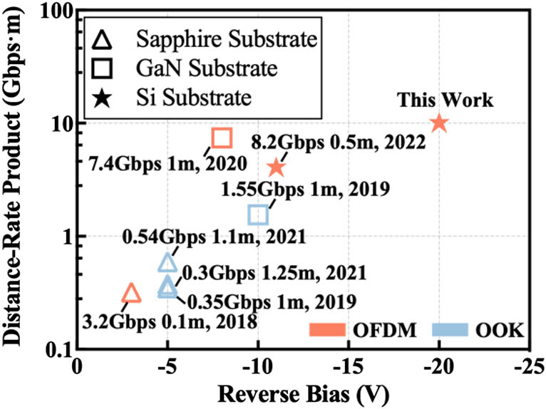
Figure 1.Benchmark of distance-rate product versus reverse bias voltage for micro-LED-based photodetectors.
However, almost all reported GaN-based μPDs are grown on sapphire substrates or GaN substrates. Due to the non-conductivity and low thermal conductivity of sapphire substrates, sapphire-based LEDs and μPDs are often fabricated in lateral structures, which can bring current crowding and current droop under a high injection current density or high incident light power. A GaN substrate is the most ideal substrate for growing GaN-based LEDs and μPDs, but it faces problems such as difficulty in production and high price for commercial use. Si substrates are another promising option to grow GaN-based LEDs or μPDs due to the advantages of low cost, large size, high crystal quality, better conductivity, and great thermal conductivity [33]. In recent years, InGaN/GaN MQW LEDs fabricated on Si (111) (Si-substrate LED) have shown impressive results as transmitting devices in high-speed VLC systems [8,34]. Nevertheless, as a receiving device, a Si-substrate MSM UV PD is proposed, but the transmission performance in VLC links has yet to be experimentally investigated [35]. Our previous work has experimentally demonstrated for the first time the possibility of Si-substrate LEDs as PDs [36].
In this paper, an InGaN/GaN MQW-based vertical-structure micro-LED-based PD on a Si substrate is proposed and fabricated. The photoelectrical performances of three different sizes of our designed μPDs are investigated, including 10, 50, and 100 μm. The peak responsivity of all three μPDs is achieved at 400 nm, while the passband full-widths at half maximum (FWHMs) are 87 nm (375–462 nm), 72 nm (382–454 nm), and 78 nm (382–460 nm) for 10, 50, and 100 μm μPDs, respectively. Such large FWHMs provide the feasibility of μPDs as a receiver in WDM VLC systems. Utilizing the self-designed
2. FABRICATION AND CHARACTERIZATION
A. Design and Fabrication of Si-Substrate Micro-LED-Based Photodetector
In this experiment, we fabricate vertical GaN-based micro-LEDs on Si substrates. Considering the triangular symmetry relationship between the Si (111) and GaN (0001) planes, the Si (111) substrate is the best choice for the growth of c-plane GaN [37]. The proposed micro-LED samples are grown on a patterned Si (111) substrate by a self-developed metalorganic chemical vapor deposition (MOCVD) reactor. Trimethylaluminum (TMAl), trimethylgallium (TMGa), trimethylindium (TMIn), and ammonia (
After epitaxial growth, the epitaxial wafer is fabricated into
![]()
Figure 2.(a) Schematic of the vertical structure of Si-substrate micro-LED-based photodetector; SEM images of (b) 10 μm, (c) 50 μm, and (d) 100 μm chips.
On the basis of the above micro-LED chips,
![]()
Figure 3.(a) Schematic of layout for
B. Optical and Electrical Characteristics
We begin by evaluating the optical and electrical characteristics of three micro-LEDs. Figures 4(a), 4(b), and 4(c) show the responsivity spectra of 10, 50, and 100 μm micro-LED-based PDs under different reverse bias voltages, respectively. The micro-LED chips are illuminated by monochromatic light from a 250 W xenon lamp (350–700 nm) passing through a monochromator (Newport CS260-USB-2-MT-D). The peak responsivity of all three μPDs is achieved at 400 nm. As the reverse bias voltage increases, the wavelength selectivity does not drift, but only increases the response intensity. The FWHMs are 87 nm (375–462 nm), 72 nm (382–454 nm), and 78 nm (382–460 nm) for 10, 50, and 100 μm μPDs, respectively. Such large wavelength selection ranges greatly increase the feasibility of μPDs as visible light receivers for WDM systems.
![]()
Figure 4.Responsivity spectra of (a) 10 μm, (b) 50 μm, and (c) 100 μm micro-LED-based photodetectors; electroluminescence spectra of (d) 10 μm, (e) 50 μm, and (f) 100 μm micro-LEDs.
The emission spectra of micro-LEDs are also measured by a high-sensitivity spectrometer (Ocean Insight QE Pro-ABS) under various driven currents, as shown in Figs. 4(d)–4(f). The emission peak appears blueshifted as the injected current increases, which is due to the band filling effect [43]. At low current density, the emission peak wavelengths are 626, 596, and 600 nm for 10, 50, and 100 μm micro-LEDs, respectively. At high current density, they can be 582, 573, and 577 nm, respectively. The difference between the peak response wavelength and peak emission wavelength is due to the different locations of light absorption and light emission.
![]()
Figure 5.Current–voltage (
3. PRINCIPLE AND EXPERIMENTAL SETUP
A. Principle of Operation
DMT modulation is a straightforward way to achieve real-value OFDM modulation, especially for VLC [8,34]. The advantage of multi-carrier modulation is that bit and power loading can be applied. The Levin–Campello (LC) algorithm is a classical bit and power joint optimization method that achieves maximum transmission rate at a certain power [44,45]. Another approach to improve the spectral efficiencies (SEs) of VLC is to use a pre-equalization circuit. Experiments have demonstrated that the modulation bandwidth can be increased from several tens of megahertz to 400–500 MHz using a suitable circuit, such as a T-bridge passive resonant circuit [46–48]. However, such a T-bridge structure circuit is limited by the device bandwidth, which can pose a hardware challenge when the modulation bandwidth is increased. Another challenge is that the analog domain hardware pre-equalization circuit does not facilitate adaptive changes. Therefore, considering that hardware equalization is changing the frequency domain response, the linear digital domain pre-equalizer method is proposed to emulate the hardware pre-equalization circuit. A better data rate performance with the digital pre-equalizer is experimentally demonstrated.
The digital signal processing (DSP) implemented in this experiment is shown in Fig. 6. The whole transmission process is divided into an SNR estimation phase and a bit power loading phase. A quadratic phase-shift keying (QPSK) signal is used to estimate the SNR at every subcarrier. The total number of subcarriers is 1024, containing the signal (512 subcarriers) and its conjugate symmetry to form Hermitian symmetry. Zero padding subcarriers are also utilized in the low-frequency portion of the signal to avoid the influence of devices similar to a bias tee, and the number is eight. Before inverse fast Fourier transform (IFFT), the signal is unsampled by a factor of two. The generated DMT signal
![]()
Figure 6.Experimental setup of VLC system utilizing micro-LED-based photodetector.
Then the signal is processed in a digital pre-equalizer process with the following expression:
Here, we redefine the hardware parameters by frequency domain equalized bandwidth
At the receiver side, standard DMT demodulation is implemented. The channel recovery algorithm is a zero-forcing algorithm based on the training sequence. During the SNR estimation phase, the SNR for each subcarrier is determined by the constellation point-based error vector magnitude (EVM) [50]. At the bit power loading phase, the bit error rate (BER) is calculated after QAM de-mapping.
In the whole experiment, the SNR table used corresponds to the HD-FEC threshold of
B. Experimental Setup
Figure 6 shows the experimental setup of a 1 m VLC system utilizing a micro-LED-based PD. The transmitted DMT signal is generated by an offline MATLAB program and an AWG (Agilent M8190A). During the whole experiment, the sampling rate of AWG is set from 4.8 to 8.2 GSa/s. A 2.5 GHz EA (Mini-Circuits ZFL-2500VH+) and a 4.2 GHz bias tee (Mini-Circuits ZFBT-4R2GW-FT+) are employed to amplify the signal and drive the 450 nm LD (OSRAM PL450B). The LD is mounted on a compact optical platform and can be configured to form a tricolor LD [12]. In the entire experiment, we transmitted 0.5 and 1 m of free space.
At the receiver side, an adjustable neutral density (ND, Daheng Optics GCO-0702M) filter is used to control the light power incident into the PD. A lens (Olympus PLN10X/0.25) is utilized to facilitate the coupling of the optical signal into the micro-LED. The micro-LED-based PD is driven with reverse bias voltage provided by a constant-current source (Keithley 2400) and a 4.2 GHz bias tee. The output signal is again amplified by a 2.5 GHz EA and then sampled by the oscilloscope (OSC, Agilent MSO9254A). The sampling rate of the OSC is set at 5 GSa/s.
The entire DSP section is a standard bit-power loading DMT based on the LC algorithm, except for the use of a digital pre-equalizer. The specific processes can be found in the previous subsection. It is worth mentioning that the digital pre-equalizer process involves the optimization of specific parameters since it simulates a hardware pre-equalization circuit. For example, at a baudrate of 1.8 Gbaud,
4. EXPERIMENTAL RESULTS AND DISCUSSION
A. System Optoelectronic Performance
First, we investigate the system’s optoelectronic performance based on the setup in Fig. 6. The transmission distance is 0.5 m to simplify alignment and avoid channel effects on measurement performance. The frequency responses of the system with three micro-LEDs are measured using a network analyzer (Agilent N5230C), as shown in Figs. 7(a)–7(c). As can be seen from the results, the absolute values of the responses of all three sizes of micro-LEDs increase as the reverse bias voltage rises. At the same time, the bandwidth is also increasing with the voltage. The
![]()
Figure 7.Measured forward transmission gains of (a) 10 μm, (b) 50 μm, and (c) 100 μm micro-LED-based photodetectors; (d) 10 and 20 dB bandwidths versus reverse bias.
To further explore the SNRs of the three μPDs, the SNR performance is measured at 1 GHz bandwidth DMT signal. The results are presented in the form of box plots in Fig. 8. It shows the maximum, minimum, median, upper quartile, and lower quartile of the SNRs of the subcarriers at different voltages. As the reverse bias voltage increases, the maximum, minimum, and median SNRs increase for all three μPDs. The maximum-minimum SNR difference for both 10 and 100 μm is greater than for 50 μm, which is due to the fact that there has been some degradation in the high-frequency response at 1 GHz bandwidth for these two μPDs. Comparing the box size of the upper and lower quadrants, we can find that the communication performance of the 10 μm μPD should be better than the 100 μm one, but much worse than the 50 μm μPD.
![]()
Figure 8.SNR versus reverse bias for (a) 10 μm, (b) 50 μm, and (c) 100 μm micro-LED-based photodetectors.
B. Performance of High-Speed Communication System
In this section, we investigate the transmission performances of μPDs. Figure 9 shows the variation of data rate with the peak-to-peak voltage (Vpp) and the bias current of an LD at 0.5 m transmission distance. The sampling rates for 10, 50, and 100 μm are set at 5.2, 7.6, and 5.2 GSa/s, respectively. The reverse bias voltages of all μPDs operate at
![]()
Figure 9.Data rate versus bias current and signal Vpp for (a) 10 μm, (b) 50 μm, and (c) 100 μm micro-LED-based photodetectors.
Figure 10(a) shows the data rate versus reverse bias voltage for 10, 50, and 100 μm μPDs. The results demonstrate that as the bias voltage rises, the transmission rate rises sharply and then tends to level off. Although GaN, as a wideband semiconductor, can support higher reverse bias voltages to obtain detection gain, in this experiment, the reverse bias voltage is only up to
![]()
Figure 10.(a) Data rate versus reverse bias; (b) data rate versus incident light power for 10, 50, and 100 μm micro-LED-based photodetectors.
To analyze the reception performance of μPDs, we measure the relationship between incident light power and transmission data rates. The incident light power is controlled by the adjustable ND placed in front of the lens. The optical density (OD) parameter of the ND is 0–1.5, which means that the optical power can be attenuated to a minimum of 3% of the initial optical power. An integrating sphere photodiode power sensor (Thorlabs S142C) is utilized to measure the attenuated optical power. The results are shown in Fig. 10(b). According to the measured results, the optimal incident optical power for both 50 and 100 μm μPDs requires only about 60 mW, and higher optical power cannot improve the transmission rate. For the 10 μm μPD, the transmission rate still increases as the incident optical power increases. This is because even though the lens used is already an objective lens, the converged spot may still be larger than 10 μm, resulting in not all of the incident optical power being received by the μPD. This also illustrates that smaller μPD sizes make alignment more difficult. When the incident light power is minimized to 4.68 mW, the rates of 10, 50, and 100 μm μPDs are 3.65, 6.41, and 4.15 Gbps, respectively.
We further investigated the relationship between bandwidth and data rate. To transmit high-speed signals, a digital pre-equalizer is employed to simulate a hardware pre-equalization circuit. Figures 11(a)–11(c) show the electrical spectra of the original signal (without the digital pre-equalizer), transmitted signal, and received signal. The sampling rates for 10, 50, and 100 μm are set at 4.8, 7.6, and 4.8 GSa/s, respectively. The baudrates are 1.2, 1.9, and 1.2 Gbaud, respectively. Considering zero padding, the effective signal bandwidths are 0.021–1.2, 0.033–1.9, and 0.021–1.2 GHz, respectively. As can be seen from the transmitted signal spectrum, the digital pre-equalizer slightly reduces the low-frequency component signal, with a 12 dB reduction in the lowest-frequency component. Even so, the spectrum of the received signal still shows that the low frequency is higher than the high frequency. The result of such a pre-compensation is also taken into account, in that overcompensation can lead to degradation of system performance [52]. Both the 10 and 100 μm spectra start to drop off quickly and rapidly around 700 MHz, which is roughly near the
![]()
Figure 11.Measured electrical spectra for (a) 10 μm, (b) 50 μm, and (c) 100 μm micro-LED-based photodetectors; maximum data rate and BER versus baudrate at 0.5 m for (d) 10 μm, (e) 50 μm, and (f) 100 μm micro-LED-based photodetectors.
Figures 11(d)–11(f) illustrate the relationship between baudrate and data rate. The baudrate ranges from 1.2 to 1.6 Gbaud for 10 and 100 μm μPDs, and from 1.7 to 2.1 Gbaud for the 50 μm μPD. As the modulation bandwidth increases, the rate gradually reaches its highest point and then starts to decrease. The maximum data rate for the 10 μm μPD is 7.58 Gbps with 1.5 Gbaud, while it is 10.81 Gbps with 1.9 Gbaud for the 50 μm μPD and 7.18 Gbps with 1.4 Gbaud for the 100 μm μPD. The BER for each transmission data rate is under the HD-FEC threshold of
Finally, to show the effect of distance on data rate and to facilitate comparison with related work, a 1 m free space VLC transmission experiment is demonstrated using the 50 μm μPD at 1.9 Gbaud. Figure 12 shows the performance results. As the transmission distance increases from 0.5 to 1 m, the transmission rate decreases only slightly, from 10.81 to 10.14 Gbps. The calculated BERs are
![]()
Figure 12.Data rate and BER versus transmission distance for 50 μm micro-LED-based photodetector.
The detailed bit and power allocations of 0.5 and 1 m are shown in Fig. 13. In Fig. 13(a), the achievable average SE is
![]()
Figure 13.SNR and bit number versus frequency at 1.9 Gbaud for (a) 0.5 m and (b) 1 m transmission distance; power ratio versus frequency for (c) 0.5 m and (d) 1 m.
To compare the results of recent micro-LED-based PDs, we have summarized the relevant results, as shown in Table 2. Neither the sapphire-substrate nor the GaN-substrate μPDs have achieved transmission rates above 10 Gbps. This is probably due to the low thermal conductivity of the sapphire substrate when high incident light power is present, which results in current crowding and current droop. GaN substrates, on the other hand, have the potential for high speed, but may require better chip design. In addition, the SE of OOK modulation is too low compared to OFDM modulation to achieve high-speed transmission. Compared with the results for a transmission distance of 1 m and transmission rate of 7.4 Gbps [28], the present work increases the data rate by approximately 3Gbps for the same transmission distance, using the similar bit power loading multicarrier modulation method. The 72 nm FWHM significantly enhances the feasibility of μPDs in VLC systems. To the best of our knowledge, this is the highest transmission rate for InGaN/GaN micro-LED-based PDs, and the first time that a data rate of 10 Gbps has been reached. Furthermore, it is anticipated that such a high-speed μPD will also be accessible as a high-speed transmitter, which has the potential to allow the design of transmitter chips and receiver chips to learn from each other.
Recent Achievements of Micro-LED-Based Photodetectors
| Year | Substrate | Array | Bias | Peak Response | FWHM | Modulation | Data Rate | Distance | Reference |
|---|---|---|---|---|---|---|---|---|---|
| 2018 | Sapphire | – | −3 V | 392 nm | 34 nm | OFDM | 3.2 | 0.5 m fiber and 0.1 m free space | [ |
| 2019 | Sapphire | Not mentioned | −5 V | 405 nm | – | OOK | 0.35 | 1 m free space | [ |
| 2019 | GaN | – | −10 V | 400 nm | 40 nm | OOK | 1.55 | 1 m free space | [ |
| 2020 | GaN | – | −8 V | 400 nm | 60 nm | BPL-OFDM | 7.4 | 1 m free space | [ |
| 2021 | Sapphire | Not mentioned | −5 V | – | – | OOK | 0.06 | 2.3 m underwater | [ |
| 2021 | Sapphire | −5 V | – | – | OOK | 0.3 | 1.25 m free space | [ | |
| 2021 | Sapphire | −5 V | – | – | OOK | 0.54 | 1.1 m free space | [ | |
| 2022 | Si | −20 V | 425 nm | – | BPL-OFDM | 8.205 | 0.5 m free space | [ | |
| 2022 | Si | −20 V | 400 nm | 72 nm | BPL-DMT | 10.14 | 1 m free space | This work |
5. CONCLUSION
In this paper, an InGaN/GaN MQW-based vertical-structure μPD on a Si substrate is proposed as a receiver to achieve a 10 Gbps VLC system with a 450 nm LD. The photoelectrical performances of our constructed μPDs of three various sizes, 10, 50, and 100 μm, are investigated. At low current density, the emission peak wavelengths are 626, 596, and 600 nm for 10, 50, and 100 μm micro-LEDs, respectively. As a receiver, the peak responsivity of all three μPDs is achieved at 400 nm, while the passband FWHMs are 87 nm (375–462 nm), 72 nm (382–454 nm), and 78 nm (382–460 nm) for 10, 50, and 100 μm μPDs. Unfortunately, the bandwidth of our device is limited mainly by the RC delay, although this can be addressed in the future via package optimization and better chip fabrication. Utilizing the self-designed
References
[2] M. Latva-aho, K. Leppänen, F. Clazzer, A. Munari. Key Drivers and Research Challenges for 6G Ubiquitous Wireless Intelligence(2019).
[14] J. Lavrencik, S. Varughese, V. A. Thomas, G. Landry, Y. Sun, R. Shubochkin, K. Balemarthy, J. Tatum, S. E. Ralph. 4
[30] Y.-H. Chang, F.-J. Liou, W. H. Gunawan, C.-W. Chow, Y. Liu, H.-C. Kuo, C.-H. Yeh. High bandwidth semipolar (20-21) μ-LED serving as photo-receiver for visible light communication. European Conference on Optical Communication (ECOC), 1-4(2021).
[36] W. Niu, J. Shi, Z. Xu, D. Li, W. Xiao, G. Wang, J. Zhang, Z. He, C. Shen, N. Chi. 8.205-Gbit/s visible light communication utilizing 4 × 4 Si-substrate μLED-based photodetector array. Optical Fiber Communication Conference, Tu3C.2(2022).
[42] F. Jiang, L. Wang, W. Fang. Semiconductor light-emitting device and method for making same. U.S. patent(2011).
[44] J. Campello. Practical bit loading for DMT. IEEE International Conference on Communications, 801-805(1999).
[45] J. Campello. Optimal discrete bit loading for multicarrier modulation systems. IEEE International Symposium on Information Theory, 193(1998).
[50] R. A. Shafik, M. S. Rahman, A. R. Islam. On the extended relationships among EVM, BER and SNR as performance metrics. International Conference on Electrical and Computer Engineering (ICECE), 408-411(2006).


Set citation alerts for the article
Please enter your email address

© Copyright 2018-2021 | Chinese Laser Press. All Rights Reserved 沪ICP备15018463号-20