• Journal of Semiconductors
  • Vol. 40, Issue 6, 062003 (2019)
Hua Pang1, Jiahuan Yan1, Jie Yang1, Shiqi Liu1, Yuanyuan Pan1, Xiuying Zhang1, Bowen Shi1, Hao Tang1, Jinbo Yang1、2, Qihang Liu3, Lianqiang Xu4, Yangyang Wang5, and Jing Lv1、2、6
Author Affiliations
  • 1State Key Laboratory for Mesoscopic Physics and Department of Physics, Peking University, Beijing 100871, China
  • 2Collaborative Innovation Center of Quantum Matter, Beijing 100871, China
  • 3Shenzhen Institute for Quantum Science and Technology and Department of Physics, Southern University of Science and Technology, Shenzhen 518055, China
  • 4School of Physics and Electronic Information Engineering, Engineering Research Center of Nanostructure and Functional Materials, Ningxia Normal University, Guyuan 756000, China
  • 5Nanophotonics and Optoelectronics Research Center, Qian Xuesen Laboratory of Space Technology, China Academy of Space Technology, Beijing 100094, China
  • 6Beijing Key Laboratory for Magnetoeletric Materials and Devices (BKL-MEMD), Beijing 100871, China
  • show less
    DOI: 10.1088/1674-4926/40/6/062003 Cite this Article
    Hua Pang, Jiahuan Yan, Jie Yang, Shiqi Liu, Yuanyuan Pan, Xiuying Zhang, Bowen Shi, Hao Tang, Jinbo Yang, Qihang Liu, Lianqiang Xu, Yangyang Wang, Jing Lv. Bilayer tellurene–metal interfaces[J]. Journal of Semiconductors, 2019, 40(6): 062003 Copy Citation Text show less
    (Color online) (a) Top-view and (b) side-view of bilayer (BL) tellurene structure. Brown balls represent the contact layer while the orange ones represent the noncontact layer. (c) Schematic diagram of the interface when the BL tellurene atoms contact with metal surface. Green balls stand for the contacting metal atoms.
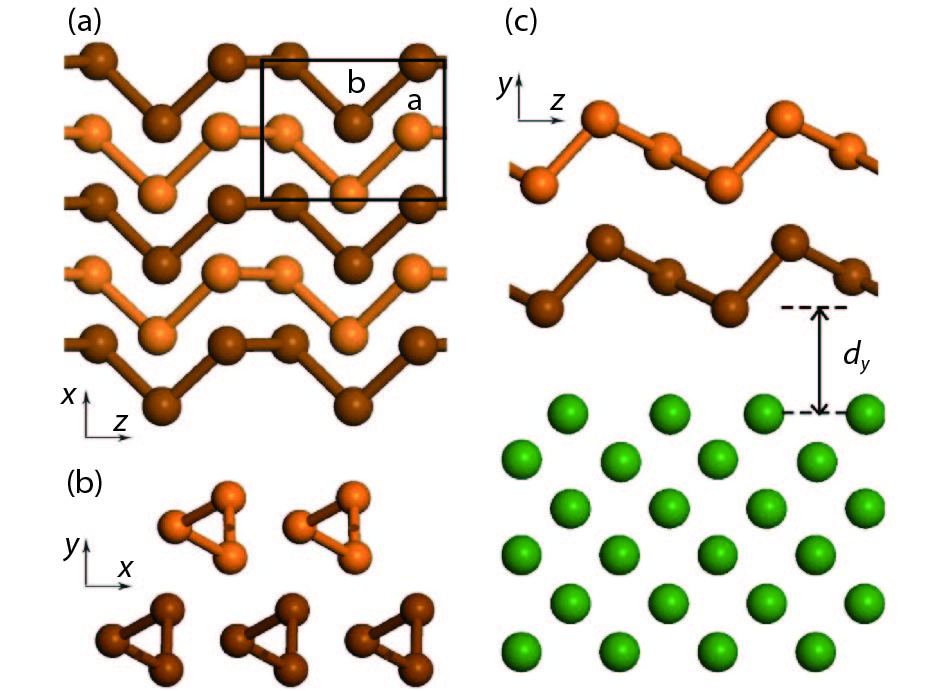
    Fig. 1. (Color online) (a) Top-view and (b) side-view of bilayer (BL) tellurene structure. Brown balls represent the contact layer while the orange ones represent the noncontact layer. (c) Schematic diagram of the interface when the BL tellurene atoms contact with metal surface. Green balls stand for the contacting metal atoms.
    (Color online) Schematic diagram of the BL tellurene FET. Schottky barriers may arise at the interfaces represented by dashed lines in two directions.
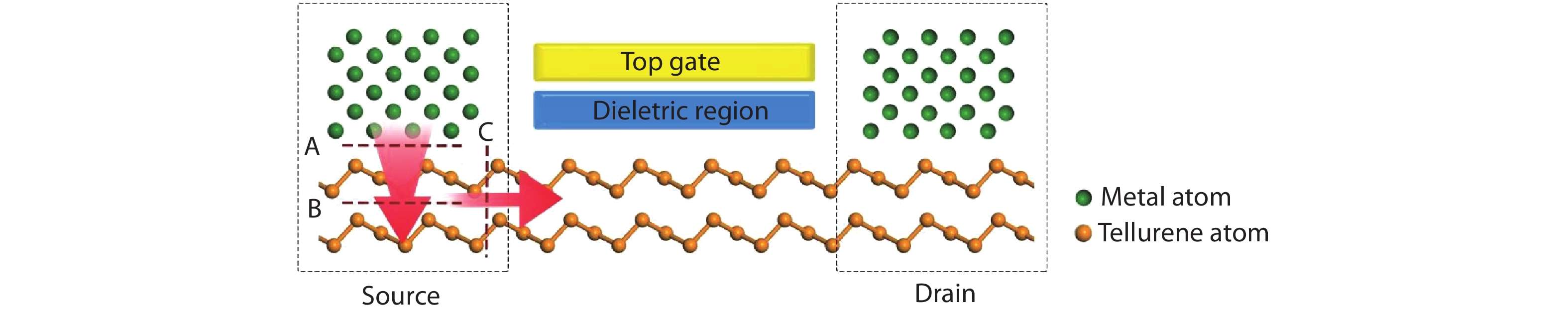
    Fig. 2. (Color online) Schematic diagram of the BL tellurene FET. Schottky barriers may arise at the interfaces represented by dashed lines in two directions.
    (Color online) Side-views of the calculated stable BL tellurene–Ag, Al, Ni, Au, Pd, Pt, Cu and graphene contacts. Brown balls are tellurene atoms, while other colored balls are metal and graphene atoms. The diagram of average potential distribution is inset in the black box, where the Fermi level is set to zero with the red dash lines and the tunneling barrier ΔV is shown by the black arrows.
    Fig. 3. (Color online) Side-views of the calculated stable BL tellurene–Ag, Al, Ni, Au, Pd, Pt, Cu and graphene contacts. Brown balls are tellurene atoms, while other colored balls are metal and graphene atoms. The diagram of average potential distribution is inset in the black box, where the Fermi level is set to zero with the red dash lines and the tunneling barrier ΔV is shown by the black arrows.
    (Color online) (a) Band structure of the BL tellurene. (b)–(i) Band structure of the BL tellurene-metal systems (projected to the bilayer tellurene). The Fermi level is set at zero and represented by the dashed lines. Gray lines: the band structure of the composite system. The red lines reflect the band structure of the tellurene layer away from the metal surface (the noncontact tellurene layer), the blue ones reflect the band structure of the tellurene layer near the metal surface (the contact tellurene layer). The line width is proportional to its weight.
    Fig. 4. (Color online) (a) Band structure of the BL tellurene. (b)–(i) Band structure of the BL tellurene-metal systems (projected to the bilayer tellurene). The Fermi level is set at zero and represented by the dashed lines. Gray lines: the band structure of the composite system. The red lines reflect the band structure of the tellurene layer away from the metal surface (the noncontact tellurene layer), the blue ones reflect the band structure of the tellurene layer near the metal surface (the contact tellurene layer). The line width is proportional to its weight.
    (Color online) (a) Part density of states (PDOS) of BL tellurene. (b)–(i) PDOS of each orbital for BL tellurene on the metal surface by the band calculations. Solid lines represent for the PDOS of the contact tellurene layer, while dash lines represent for the PDOS of the noncontact tellurene layer.
    Fig. 5. (Color online) (a) Part density of states (PDOS) of BL tellurene. (b)–(i) PDOS of each orbital for BL tellurene on the metal surface by the band calculations. Solid lines represent for the PDOS of the contact tellurene layer, while dash lines represent for the PDOS of the noncontact tellurene layer.
    (Color online) Localized density of states (LDDOS) of the BL tellurene FET devices with metals Al, Ag, Ni, Au, Pd, Pt, Cu and graphene as electrodes (left panel) with a 5-nm channel length as well as the zero-bias transmission spectrum of the FET devices (right panel). Metal-induced gap states at the interfaces are indicated by the black dashed lines, and the Fermi level is represented by white and red dashed lines.
    Fig. 6. (Color online) Localized density of states (LDDOS) of the BL tellurene FET devices with metals Al, Ag, Ni, Au, Pd, Pt, Cu and graphene as electrodes (left panel) with a 5-nm channel length as well as the zero-bias transmission spectrum of the FET devices (right panel). Metal-induced gap states at the interfaces are indicated by the black dashed lines, and the Fermi level is represented by white and red dashed lines.
    (Color online) (a) Comparison of the electron and hole SBHs of the BL tellurene FETs obtained by work function approximation () and quantum transport simulation methods in the lateral direction. (b) Lateral SBH as a function of the electrode material’s work function. The blue and pink lines indicate the fitting lines for the SBHs of the electrons for work function approximation and quantum transport simulation, respectively. The pink transparent ellipse represents for the minimal ellipse area that can overcome all the electron SBHs of the bulk metallic electrode cases for the quantum transport calculations. (c) Schematic plot of the Fermi level pinning (FLP) in the BL tellurene transistors.
    Fig. 7. (Color online) (a) Comparison of the electron and hole SBHs of the BL tellurene FETs obtained by work function approximation ( ) and quantum transport simulation methods in the lateral direction. (b) Lateral SBH as a function of the electrode material’s work function. The blue and pink lines indicate the fitting lines for the SBHs of the electrons for work function approximation and quantum transport simulation, respectively. The pink transparent ellipse represents for the minimal ellipse area that can overcome all the electron SBHs of the bulk metallic electrode cases for the quantum transport calculations. (c) Schematic plot of the Fermi level pinning (FLP) in the BL tellurene transistors.
    (Color online) FLP factor (S ) as a function of two-dimensional channel materials’ band gap. R represents for the linear correlation coefficient, where ML black phosphorene and MoS2 are not included.
    Fig. 8. (Color online) FLP factor (S ) as a function of two-dimensional channel materials’ band gap. R represents for the linear correlation coefficient, where ML black phosphorene and MoS2 are not included.
    MetalAgAlNiAuPdPtCuGraphene
    represents for the average mismatch ratio of the lattice parameter of metal. is the average distance between the contact tellurene layer and the contacted metal layer for the vertical direction. Tunneling barrier height ΔV, which is defined as the potential energy above the Fermi energy Ef at the interfaces. is the minimal atom-to-atom distance between tellurene atom and metal atom. Binding energy is the energy taken to remove per tellurene atom from the metal surface. and are the calculated wave function of the free-standing metal or graphene surface and the composite system. () is the electron (hole) SBH acquired from the wave function approximation (WFA) method for the lateral direction, while () is the electron (hole) Schottky barrier height (SBH) acquired by the quantum transport simulation (QTS) method for the lateral direction. is the transport gap of the BL tellurene FET.
    (%) 2.423.042.582.554.704.665.002.28
    (Å) 1.402.121.661.671.741.731.732.95
    (Å) 2.812.642.442.742.602.642.493.55
    ΔV (eV) –13.29–6.3–12.08–9.18–13.21–12.42–11.21–1.09
    (eV) 0.740.961.290.941.171.100.770.51
    (eV) 4.194.285.014.965.125.654.654.58
    (eV) 4.254.344.524.424.614.784.674.74
    0.230.320.500.400.590.720.65
    0.730.640.460.560.370.240.31
    0.390.380.390.390.400.440.510.53
    0.350.320.310.290.290.250.190.08
    0.740.700.700.780.690.690.700.61
    Table 1. Calculated data of the interface with bilayer tellurene on various kinds of metals.
    Hua Pang, Jiahuan Yan, Jie Yang, Shiqi Liu, Yuanyuan Pan, Xiuying Zhang, Bowen Shi, Hao Tang, Jinbo Yang, Qihang Liu, Lianqiang Xu, Yangyang Wang, Jing Lv. Bilayer tellurene–metal interfaces[J]. Journal of Semiconductors, 2019, 40(6): 062003
    Download Citation