• Journal of Semiconductors
  • Vol. 40, Issue 6, 062003 (2019)
Hua Pang1, Jiahuan Yan1, Jie Yang1, Shiqi Liu1, Yuanyuan Pan1, Xiuying Zhang1, Bowen Shi1, Hao Tang1, Jinbo Yang1、2, Qihang Liu3, Lianqiang Xu4, Yangyang Wang5, and Jing Lv1、2、6
Author Affiliations
  • 1State Key Laboratory for Mesoscopic Physics and Department of Physics, Peking University, Beijing 100871, China
  • 2Collaborative Innovation Center of Quantum Matter, Beijing 100871, China
  • 3Shenzhen Institute for Quantum Science and Technology and Department of Physics, Southern University of Science and Technology, Shenzhen 518055, China
  • 4School of Physics and Electronic Information Engineering, Engineering Research Center of Nanostructure and Functional Materials, Ningxia Normal University, Guyuan 756000, China
  • 5Nanophotonics and Optoelectronics Research Center, Qian Xuesen Laboratory of Space Technology, China Academy of Space Technology, Beijing 100094, China
  • 6Beijing Key Laboratory for Magnetoeletric Materials and Devices (BKL-MEMD), Beijing 100871, China
  • show less
    DOI: 10.1088/1674-4926/40/6/062003 Cite this Article
    Hua Pang, Jiahuan Yan, Jie Yang, Shiqi Liu, Yuanyuan Pan, Xiuying Zhang, Bowen Shi, Hao Tang, Jinbo Yang, Qihang Liu, Lianqiang Xu, Yangyang Wang, Jing Lv. Bilayer tellurene–metal interfaces[J]. Journal of Semiconductors, 2019, 40(6): 062003 Copy Citation Text show less

    Abstract

    Tellurene, an emerging two-dimensional chain-like semiconductor, stands out for its high switch ratio, carrier mobility and excellent stability in air. Directly contacting the 2D semiconductor materials with metal electrodes is a feasible doping means to inject carriers. However, Schottky barrier often arises at the metal–semiconductors interface, impeding the transport of carriers. Herein, we investigate the interfacial properties of BL tellurene by contacting with various metals including graphene by using ab initio calculations and quantum transport simulations. Vertical Schottky barriers take place in Ag, Al, Au and Cu electrodes according to the maintenance of the noncontact tellurene layer band structure. Besides, a p-type vertical Schottky contact is formed due to the van der Waals interaction for graphene electrode. As for the lateral direction, p-type Schottky contacts take shape for bulk metal electrodes (hole Schottky barrier heights (SBHs) ranging from 0.19 to 0.35 eV). Strong Fermi level pinning takes place with a pinning factor of 0.02. Notably, a desirable p-type quasi-Ohmic contact is developed for graphene electrode with a hole SBH of 0.08 eV. Our work sheds light on the interfacial properties of BL tellurene based transistors and could guide the experimental selections on electrodes.

    1. Introduction

    Two-dimensional (2D) semiconductor has been a competitive candidate of channel material of transistors for the coming sub-10 nm generation field effect transistor (FET) as they offer several advantages over traditional silicon[19]. This category holds a high immunity to short-channel effects out of their ultrathin thickness[10, 11]. Few trap states and the depressed scattering out of the roughness on the dangling bond-free flat surface significantly enhance the carrier mobility[10, 12, 13]. 2D layered phosphorene and InSe own a high carrier mobility but unfortunately they do not hold a good ambient stability[8, 14]. It is highly desirable to discover a 2D semiconductor with both high mobility and good stability. 2D PtSe2 and Bi2O2Se are reported to meet the two criteria[15, 16]. Very recently, a new 2D semiconductor, few-layer tellurene (2D tellurium) has been experimentally prepared by both molecular beam epitaxy and solution-based method[1719]. Tellurene has a layer-dependent band gap[10, 11, 13, 2022]. Notably, the most stable few-layer tellurene is comprised of one-dimensional Te spiral chains by van der Waals (vdW) forces, while the most stable monolayer (ML) tellurene takes the tetragonal phase[20, 23]. The fabricated few-layer tellurene FET exhibits a quite large switch ratio (106)[19]. Remarkably, tellurene owns both a high carrier mobility of 700 cm2V–1s–1 and high ambient stability[19]. Such characters render tellurene to surpass some stable but low-carrier-mobility 2D dichalchogenide MX2[2429] and high-carrier-mobility but air-unstable phosphorene and InSe[15, 30, 31] and become one of the most competitive 2D channel materials.

    Directly contacting the 2D semiconductor channel with metal electrode is a feasible doping means in the absence of a sustainable substitution doping method[10]. Schottky barrier is generally brought about at the interface of metal electrode and semiconductor[32, 33]. High Schottky barrier still stands in the way of the performance of 2D semiconductor based FETs[32]. In light of this, figuring out interfacial properties and accurate predictions on Schottky barrier height (SBH) is crucial in guiding the design of 2D semiconductor based transistors. However, the SBH cannot be simply achieved from the difference between the Fermi level of metal and the valence band maximum (VBM)/conduction band minimum (CBM) of the semiconductor, due to the Fermi level pinning (FLP)[3436].

    In this paper, we explore the vertical and lateral interfacial properties of BL tellurene FETs by using ab initio electronic band calculation and quantum transport simulation, which takes FLP at the interfaces into counts and presents accurate predictions on the SBH[37]. The band structures of BL tellurene exhibit various degrees of hybridization after contacting with different metal electrodes. Ohmic contacts are developed for Ni, Pd and Pt electrodes in the vertical direction due to the strong hybridization of both tellurene layers, while Schottky barriers take shape between the two tellurene layers for Ag, Al, Au and Cu electrodes as the band structure of the noncontact tellurene layer is maintained. On the contrary, the band structure of BL tellurene remains for the graphene electrode due to the weak vdW interaction. As to the lateral direction, p-type Schottky contacts are preferred with hole SBHs of 0.35, 0.32, 0.31, 0.29, 0.29, 0.25 and 0.19 eV, generated for Ag, Al, Ni, Au, Pd, Pt and Cu electrodes, respectively. On the other hand, a lateral p-type quasi-Ohmic contact takes shape with an ultralow hole SBH of 0.08 eV for graphene electrode.

    2. Models and methods

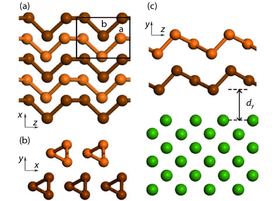
    A fully relaxed BL tellurene structure is shown in Fig. 1 with lattice constants of a = 4.32 Å and b = 5.81 Å, which is in accordance with the calculation results reported before[23]. Brown balls represent for tellurium atoms that are in direct contact with the metal atoms, and we define them as the contact tellurene layer. Their counterparts, the orange ones, are defined as noncontact tellurene layer. Inherent anisotropy is exhibited that the Te chains connected by covalent bonds are stacked by vdW forces vertically, and the bond length along a direction is relatively longer than that along b direction. Latest experiment of few-layer tellurene FET have examined the mobility of channel directions along both a and b directions. The extracted field-effect mobility along the Te chain surpass the other with an average anisotropic mobility ratio of 1.43[38]. Therefore, BL tellurene along the zigzag chain direction is applied as channel here for the consideration a better transport property. Electrode materials commonly used in experiments such as Ag, Al, Ni, Au, Pd, Pt, Cu and 2D graphene are employed[19, 39]. and they cover a wide range of work function. As shown in Fig. 1(c), six layers of bulk metal atoms (green balls) are used to imitate the metal surface, on the side of which absorbs the BL tellurene. We slightly stretch the metal lattice to adapt the fixed optimized BL tellurene unit cell with a tiny mismatch within 5%, which is shown in Table 1. We adjust the 1 × 2 Al(110)/Ag(110)/Au(110) supercell and Cu(111)/Pt(111)/Pd(111) supercell to the a× b BL tellurene supercell, and Ni(111)/ML graphene supercell to the BL tellurene, separately. The initial distance of BL tellurene and metal surface is set as 3 Å, and a vacuum zone with a length of at least 15 Å is applied for each configuration. Owing to the fact that the geometry relaxation mainly takes place at the interface, the bottom three layers of metal atoms are fixed.

    (Color online) (a) Top-view and (b) side-view of bilayer (BL) tellurene structure. Brown balls represent the contact layer while the orange ones represent the noncontact layer. (c) Schematic diagram of the interface when the BL tellurene atoms contact with metal surface. Green balls stand for the contacting metal atoms.

    Figure 1.(Color online) (a) Top-view and (b) side-view of bilayer (BL) tellurene structure. Brown balls represent the contact layer while the orange ones represent the noncontact layer. (c) Schematic diagram of the interface when the BL tellurene atoms contact with metal surface. Green balls stand for the contacting metal atoms.

    Table Infomation Is Not Enable

    We carry out density functional theory (DFT) calculations using Vienna ab initio simulation package (VASP) to complete geometric optimizations and electronic calculations[4043]. The method of projector augmented wave and a plane-wave basis set are applied here, the kinetic energy cut-off for which is set to 500 eV. It is regarded to obtain a stable structure when the residual force drops below 0.01 eV/Å and the energy is converged to within 1 × 10⁻⁵ eV for each single atom between two successive steps. K-points sampling density by a separation of 0.02 Å–1 in the Brillouin zone is adopted according to the Monkhorst-Pack method[44]. Two corrections are considered below. One is the DFT-D3 correction method of Grimme, concerning vdW interaction between the layers[45]. Dipole correction is considered as well to avoid spurious interactions of dipole moments owing to the asymmetry in z direction.

    A two-probe model is presented to simulate BL tellurene based transistor, as shown in Fig. 2. We adopt the optimized composite BL tellurene-metal systems for the source and drain regions and BL tellurene for the channel with length of 5 nm. Both electrodes are considered semi-infinite along the transport direction. Gate voltage is set to zero in our calculation. Transport simulations are carried out using DFT combining with non-equilibrium Green’s function (NEGF) method implemented in the Atomistix ToolKit (ATK) 2017 package[46, 47]. The transmission coefficient (E) (k|| is a reciprocal lattice vector point along a surface-parallel direction (orthogonal to the transmission direction) in the irreducible Brillouin zone (IBZ)) is derived by

    (Color online) Schematic diagram of the BL tellurene FET. Schottky barriers may arise at the interfaces represented by dashed lines in two directions.

    Figure 2.(Color online) Schematic diagram of the BL tellurene FET. Schottky barriers may arise at the interfaces represented by dashed lines in two directions.

    $ {T^{{k_\parallel }}}(E) = {\rm{Tr}}[\varGamma _{\rm{L}}^{{k_\parallel }}(E)G_{}^{{k_\parallel }}(E)\varGamma _{\rm{R}}^{{k_\parallel }}(E)G_{}^{{k_\parallel }{\text{†}}}(E)], $  (1)

    therein, denotes the level broadening owing to the left/right electrode and it is expressed on the basis of the electrode’s self-energy , which reflects the impact of the metal electrodes on the scattering area. Meanwhile stands for the retard (advanced) Green’s function. A double- polarized (DZP) basis set is chosen and the transmission function at given energy T(E) can be derived from the average over all in the IBZ. The real-space mesh cut-off is 75 Hartree, and room temperature by 300 K is employed[48]. Periodic boundary, Neumann boundary and Dirichlet boundary conditions are used for the x, y and z directions separately[49]. Besides, we use a Monkhorst-Pack 50 × 1 × 50 and 50 × 1 × 1 k-point grids on the electrode region and central region, respectively.

    Generalized gradient approximation (GGA) of Perdrew-Burke-Ernzerhof (PBE) parameterization form is employed throughout the paper[50]. Single electron approximation is appropriate for both the periodical interfacial system band calculation and for the FET configuration. This is due to the fact that the electron-electron interaction of both the BL tellurene under the metal electrode and at the channel is highly shielded by the doping carriers from the electrodes. Therefore, DFT-GGA method, which is based on single electron approximation, is chosen. For instance, a degenerately doped ML MoSe2 owns a band gap of 1.52 eV at the DFT-GGA level, which coincides with the band gap of 1.59 eV derived by the GW method and 1.58 eV observed in the experiments[51]. The transport band gaps of the ML, BL, trilayer (TL) phosphorene based FET with Ni electrode according to the DFT-GGA method have been calculated to be 0.79, 0.81 and 0.68 eV, which are compared with the experiment results (1.00, 0.71 and 0.61 eV)[5254].

    3. Results and discussions

    3.1. BL tellurene–metal interface

    Eight composite tellurene–metal systems have been brought up, and after structural optimization, the Al, Ag, Au, Cu and graphene interfaces are slightly distorted, while the Ni, Pd and Pt interfaces are strongly distorted, as shown in Fig. 3. The distortions are induced by the interactions between BL tellurene and metals. For the optimized system, dy is the minimal distance between the contact tellurene layer and the nearest metal layer along y direction according to Fig. 1(c), while dTe–M represents the minimal atom-to-atom distance between the Te atom and metal atom. The binding energy Eb of the composite system is estimated as

    (Color online) Side-views of the calculated stable BL tellurene–Ag, Al, Ni, Au, Pd, Pt, Cu and graphene contacts. Brown balls are tellurene atoms, while other colored balls are metal and graphene atoms. The diagram of average potential distribution is inset in the black box, where the Fermi level is set to zero with the red dash lines and the tunneling barrier ΔV is shown by the black arrows.

    Figure 3.(Color online) Side-views of the calculated stable BL tellurene–Ag, Al, Ni, Au, Pd, Pt, Cu and graphene contacts. Brown balls are tellurene atoms, while other colored balls are metal and graphene atoms. The diagram of average potential distribution is inset in the black box, where the Fermi level is set to zero with the red dash lines and the tunneling barrier ΔV is shown by the black arrows.

    $ {E_{\rm{b}}} = ({E_{{\rm{Te}}}} + {E_{\rm{M}}} - {E_{{\rm{Te - M}}}})/N, $  (2)

    where , and separately stands for the relaxed energy of the free-standing BL tellurene, the free-standing metal structure and the composite system. N is the number of the contact tellurene layer atoms that directly contact with the metal layers. Specific parameters of these eight optimized systems are given in Table 1. Three groups by different interactions at these eight interfaces are distinguished by the binding energy Eb. Graphene electrode owns the smallest Eb (0.51 eV), accompanied by the largest distance dy (2.95 Å) and dTe–M (3.55 Å), implying a weak vdW interaction. The graphene layer is slightly distorted on account of the asymmetry of the stretching of graphene lattice in different directions (Fig. 3). The second group consists of Ag, Al, Au and Cu interfaces and is characterized by moderate Eb (0.74–0.96 eV), implying a weak covalent interaction. The third group consists of Ni, Pd and Pt interfaces and is characterized by a large Eb (1.10–1.29 eV), implying a strong covalent interaction. The strength of the interaction is in accordance with the deformation level of BL tellurene (Fig. 3).

    The distinction of the last two groups could be attributed to the different configurations of the valence electron of the metal atoms. Ag (4d105s1), Al (3s23p1), Au (5d106s1), and Cu (3d104s1) atoms possess one unpaired electron. It forms no more than one covalent bond with BL tellurene, and the remnant would form the metallic bond for the metal surface. It brings about a relatively small binding energy. On the other hand, Ni (3d84s2) and Pt (5d96s1) atoms possess two unpaired electrons, and at most two covalent bonds are formed with BL tellurene correspondingly. Despite of the 4d10 valence electron configuration of free-standing Pd atom, Mulliken population analysis indicates that the Pd atom approximately owns two unpaired electrons (4d95s1) when it interacts with tellurene. The reason lies in that the s–d orbit hybridization of Pd atom gives partially unoccupied d states that could strongly interact with p states of Te. Therefore, the Pd, Pt and Ni electrodes possess large binding energies.

    We provide the energy band structures of free-standing BL tellurene and the eight interfacial systems in Fig. 4. Free-standing BL tellurene owns an indirect band gap of 0.96 eV without considering spin-orbit coupling, which keeps pace with the previous experiment result of 0.85 eV[17]. Especially we separately extract the band structure of the contact tellurene layer (blue lines) and its counterpart, the noncontact tellurene layer (red lines). All the shapes of the band structures of the contact tellurene layer are largely varied with vanishing band gaps except for the graphene electrode. However, the origin shapes and dispersion relations of the noncontact layer are relatively preserved for Ag, Al, Au and Cu electrodes, while those for Ni, Pd and Pt electrodes are not preserved. Such a difference results in an Ohmic contact between the two tellurene layers for Ni, Pd and Pt electrodes but a Schottky contact between the two tellurene layers for Ag, Al, Au and Cu electrodes. The barrier height of the Schottky contact is derived from the difference between the Fermi level and the CBM/VBM of the noncontact tellurene, which could be identified from the distinguishable red energy band of the noncontact tellurene layer (Fig. 4). There are small amounts of components of the noncontact tellurene layer lying within the band gap of the noncontact tellurene layer and are identified as metal induced interfacial states (MIGS) for bulk metal electrodes. N-type Schottky contacts are formed for Ag, Al, Au electrodes with electron SBHs of 0.54, 0.56 and 0.42 eV, respectively, while vertical p-type Schottky contacts take place with hole SBHs of 0.35 eV for Cu electrode. As to the graphene electrode, both the band structures of BL tellurene and graphene are preserved, confirming the vdW interaction between them. The Fermi level is 0.23 eV above the VBM of BL tellurene, namely a p-type Schottky contact is formed for graphene electrode. The band gap of the noncontact tellurene layer is 1.17, 1.17, 1.08 and 1.20 eV for Ag, Al, Au and Cu electrodes, respectively, and is in accordance with the band gap of ML tellurene (1.14 eV)[37]. The graphene system holds a band gap of 0.90 eV, and it is comparable with that of BL tellurene (0.96 eV).

    (Color online) (a) Band structure of the BL tellurene. (b)–(i) Band structure of the BL tellurene-metal systems (projected to the bilayer tellurene). The Fermi level is set at zero and represented by the dashed lines. Gray lines: the band structure of the composite system. The red lines reflect the band structure of the tellurene layer away from the metal surface (the noncontact tellurene layer), the blue ones reflect the band structure of the tellurene layer near the metal surface (the contact tellurene layer). The line width is proportional to its weight.

    Figure 4.(Color online) (a) Band structure of the BL tellurene. (b)–(i) Band structure of the BL tellurene-metal systems (projected to the bilayer tellurene). The Fermi level is set at zero and represented by the dashed lines. Gray lines: the band structure of the composite system. The red lines reflect the band structure of the tellurene layer away from the metal surface (the noncontact tellurene layer), the blue ones reflect the band structure of the tellurene layer near the metal surface (the contact tellurene layer). The line width is proportional to its weight.

    The distributions of the total potential of the interfacial systems, which contains Hartree potential with exchange potential and correlation potential, are presented in Fig. 3. The red dash line represents the Fermi level and the difference between the Fermi level and the vacuum level is the work function ( ) of the composite system. The tunneling barrier (ΔV) at the interface between BL tellurene and the electrode is defined as the potential energy appearing above the Fermi level. A detailed diagram with Al-BL tellurene as an example is shown in Fig. S1. The negative value of ΔV for all cases implies that electrons could transfer freely from the metal electrode to BL tellurene.

    Partial density of states (PDOS) is also plotted to further expound the interactions between BL tellurene and the electrodes. The PDOS of free-standing BL tellurene is shown in Fig. 5(a), while those of the composite systems are shown in Figs. 5(b)5(i) with the solid lines representing the contact tellurene layer ingredients and the dash lines representing the noncontact tellurene layer ingredients. For the bulk metallic electrodes, a large number of the states appear around the Fermi level of the contact layer, whereas a relatively small number of the states around the Fermi level of the noncontact layer. It further confirms a much stronger hybridization between the bulk metal electrodes with the contact tellurene layer compared with the noncontact tellurene layer. By contrast, there are no states at the Fermi level of tellurene for graphene electrode, indicating a weak vdW interaction between tellurene and graphene.

    (Color online) (a) Part density of states (PDOS) of BL tellurene. (b)–(i) PDOS of each orbital for BL tellurene on the metal surface by the band calculations. Solid lines represent for the PDOS of the contact tellurene layer, while dash lines represent for the PDOS of the noncontact tellurene layer.

    Figure 5.(Color online) (a) Part density of states (PDOS) of BL tellurene. (b)–(i) PDOS of each orbital for BL tellurene on the metal surface by the band calculations. Solid lines represent for the PDOS of the contact tellurene layer, while dash lines represent for the PDOS of the noncontact tellurene layer.

    3.2. SBH of the BL tellurene transistors

    Here a two-probe model with BL tellurene as the channel material is set up to examine the Schottky barriers in a transistor configuration, which might be formed at three interfaces as shown in Fig. 2. A vertical Schottky barrier ( ) might arise at the interface A between the contact tellurene layer and metal layer. Another vertical Schottky barrier ( ) appears at the interface B between the two tellurene layers. Besides, a lateral one ( ) might also arise at the interface C between the BL tellurene channel zone and the electrode zone.

    The vertical Schottky barrier vanishes as the contact tellurene layer are metallized for bulk metal electrodes in terms of electronic band calculations. And the localized device density of states (LDDOS) projected to the noncontact tellurene layer is carried out to demonstrate the Schottky barrier ( ) at the vertical interfaces (Fig. S2). The band gap of the noncontact tellurene of Ni, Pd and Pt electrodes vanishes, and Ohmic contact takes place. On the other hand, that of Ag, Al, Au and Cu electrodes remains, accompanied by the MIGS. The above results are in line with the electronic band calculations, but the CBM/VBM of the noncontact tellurene is hard to identify due to the interference of the MIGS, so is the vertical SBH. A p-type Schottky contact with SBH of 0.18 eV is formed for graphene electrode, which is compared with that (0.23 eV) obtained from the electronic band calculations.

    As to the lateral Schottky barrier ( ), we use two methods including the work function approximation (WFA) and the quantum transport simulation (QTS). Traditional WFA method is generally used to estimate the lateral SBH of the metalized electrode, and the electron/hole SBH is derived from the difference between the Fermi level of the optimized electrode zone and the CBM/VBM of the free-standing BL tellurene channel zone. N-type Schottky contacts are generated for Ag, Al and Au electrodes, featured by an electron SBH of 0.23, 0.32 and 0.40 eV for the lateral direction, respectively. Meanwhile p-type ones take place for Ni, Pd, Pt and Cu electrodes, featured by a hole SBH of 0.46, 0.37, 0.24 and 0.31 eV, respectively. The WFA method only gives an approximate result, owing to the neglect of the interactions between the electrode and channel.

    The QTS method is based on a two-probe model, where both the electrode and the channel parts are calculated as a whole. The method is confirmed to offer SBHs consistent with the experimental results[5355]. The LDDOS projected to BL tellurene of the BL tellurene FETs are shown in Fig. 6 so as to visualize the energy band in real space. The MIGS are also generated at the channel region, and are indicated by the black dashed lines. Under the QTS method, the transport electron (hole) SBHs are derived as the difference of the Fermi level and the VBM/CBM of the channel at the lateral interface. We obtain lateral p-type Schottky contacts for all the electrode cases, with hole SBHs of 0.35, 0.32, 0.31, 0.29, 0.29, 0.25, 0.19 and 0.08 eV for Ag, Al, Ni, Au, Pd, Pt, Cu and graphene electrodes, respectively. The zero-bias transmission spectrums of the BL tellurene FET devices are also presented in Fig, 6, and the SBHs read from the transmission spectrums are in agreement with those read from the LDDOS. The QTS method suggests that the BL tellurene based transistors tend to form lateral p-type Schottky barriers at the interfaces with above mentioned electrodes.

    (Color online) Localized density of states (LDDOS) of the BL tellurene FET devices with metals Al, Ag, Ni, Au, Pd, Pt, Cu and graphene as electrodes (left panel) with a 5-nm channel length as well as the zero-bias transmission spectrum of the FET devices (right panel). Metal-induced gap states at the interfaces are indicated by the black dashed lines, and the Fermi level is represented by white and red dashed lines.

    Figure 6.(Color online) Localized density of states (LDDOS) of the BL tellurene FET devices with metals Al, Ag, Ni, Au, Pd, Pt, Cu and graphene as electrodes (left panel) with a 5-nm channel length as well as the zero-bias transmission spectrum of the FET devices (right panel). Metal-induced gap states at the interfaces are indicated by the black dashed lines, and the Fermi level is represented by white and red dashed lines.

    The lateral SBHs obtained by the WFA and the QTS methods are compared in Fig. 7(a). Even though the QTS and WFA method provides the same contact polarity for Pt, Pd, Cu and Ni electrodes, the hole SBH differs (0.01, 0.08, 0.12 and 0.15 eV for Pt, Pd, Cu and Ni electrodes, respectively). Remarkably, the QTS and WFA methods provide opposite contact polarity for Ag, Al and Au electrodes. Opposite to the QTS method, the WFA method does not consider the interaction between the electrode and the channel. Therefore, the difference of the SBHs revealed by those two methods lies on the interaction between the electrode and channel parts. Here we state the interaction to two aspects. First, the contact between the channel and electrode gives rise to abundant interfacial states, which are indicated by the black dashed lines in the LDDOS diagram of Fig. 6. Considering that there is no termination of BL tellurene crystal structure at the interface and the flat surface of 2D semiconductor, those interfacial states are not induced by defects, dangling bonds or the termination of tellurene structure. Therefore, they are mainly induced by metal-induced interfacial states (MIGS) that exponentially damp when penetrating into BL tellurene from metals. The MIGS would bring about intense Fermi pinning effect, thus modulate the Fermi level of the system and the SBHs. Second, the contact between the drain/source and channel regions also gives rise to a charge transfer or a charge redistribution, which induces a dipole field. The built-in field makes a relative movement between the Fermi level of the electrode and the band structure of the BL tellurene and changes the SBH. Therefore, SBHs obtained by quantum transport simulation differ from the ones obtained by work function approximation due to the coupling between the channel and electrode.

    (Color online) (a) Comparison of the electron and hole SBHs of the BL tellurene FETs obtained by work function approximation () and quantum transport simulation methods in the lateral direction. (b) Lateral SBH as a function of the electrode material’s work function. The blue and pink lines indicate the fitting lines for the SBHs of the electrons for work function approximation and quantum transport simulation, respectively. The pink transparent ellipse represents for the minimal ellipse area that can overcome all the electron SBHs of the bulk metallic electrode cases for the quantum transport calculations. (c) Schematic plot of the Fermi level pinning (FLP) in the BL tellurene transistors.

    Figure 7.(Color online) (a) Comparison of the electron and hole SBHs of the BL tellurene FETs obtained by work function approximation ( ) and quantum transport simulation methods in the lateral direction. (b) Lateral SBH as a function of the electrode material’s work function. The blue and pink lines indicate the fitting lines for the SBHs of the electrons for work function approximation and quantum transport simulation, respectively. The pink transparent ellipse represents for the minimal ellipse area that can overcome all the electron SBHs of the bulk metallic electrode cases for the quantum transport calculations. (c) Schematic plot of the Fermi level pinning (FLP) in the BL tellurene transistors.

    The transport energy gap Eg is defined as , and the calculated transport energy gap of Ag, Al, Ni, Au, Pd, Pt, Cu and graphene electrodes is 0.74, 0.70, 0.70, 0.78, 0.69, 0.69, 0.70, and 0.61 eV separately (Table 1), which are comparable with the experimental gap of 0.85 eV on graphene/6H-SiC (0001) substrate via scanning tunneling spectra measurement[17].

    The FLP effect is measured by the pinning factor S, which is the slope of the relationship between the lateral electron SBH and the work function of the bulk metal electrodes. S = 1 denotes a no FLP case while S = 0 denotes a full FLP case. Here we plot the lateral electron SBHs as a function of the metal work function, as shown in Fig. 7(b). The fitting lines are shown of the two methods leaving out the graphene cases. An extremely low pinning factor of Sa = 0.02 is obtained by the QTS method, that is much smaller that of the WFA method (Sb = 0.29). It indicates that the consideration of the interaction between the BL tellurene channel and the electrode will induce further FLP effect. What’s more, the pinning factor of BL tellurene is smaller than that of ML tellurene (S = 0.09), ML black phosphorene (S = 0.28) and ML MoS2 (S = 0.27) as well[37, 52, 56],indicating an extremely intense Fermi level pinning. The pinning effect is demonstrated in Fig. 7(c), and the Fermi level is highly pinned to a small region in the band gap of the BL tellurene.

    The ultralow S (0.02) could be inferred by the deep-into-channel MIGS in the narrow band gap. Here we plot the fitting line of the S and the band gap of the 2D channel material, as shown in Fig. 8. The calculated pinning factors of various 2D material containing blue phosphorene (0.42), arsenene (0.33), InSe (0.32), black phosphorene (0.28), MoS2 (0.1), Bi2O2Se (0.12), ML tellurene (0.09) and BL tellurene (0.02) are presented here[37, 52, 55, 5760]. An linear relationship of S = 0.48Eg –0.45 is observed, leaving out black phosphorene and MoS2, with linear correlation coefficient R2 = 0.99). This trend could deduce that under normal circumstances, a narrow band gap would give rise to an intensive distribution of the MIGS. It brings about an intensive Fermi level pinning and robust SBHs. Therefore, a small S is expected in the case of a small band gap in terms of . However, the pinning factor S depends on the selection of the metal electrode and the contact details, e. g. the orientation of the metal electrodes. Therefore the scale factor and even the linearity probably would change as the range of the metal electrode and the contact details change. The abnormal pinning factors for ML MoS2 and black phosphorene couldn’t fit in the linear relationship[52, 59]. The correlation coefficient R2 would drop to 0.44 with these two considered.

    (Color online) FLP factor (S ) as a function of two-dimensional channel materials’ band gap. R represents for the linear correlation coefficient, where ML black phosphorene and MoS2 are not included.

    Figure 8.(Color online) FLP factor (S ) as a function of two-dimensional channel materials’ band gap. R represents for the linear correlation coefficient, where ML black phosphorene and MoS2 are not included.

    Our study indicates that the BL tellurene based transistors favor p-type Schottky contacts for the lateral direction, and this is owing to the small work function (4.51 eV) of BL tellurene. Experimentally, a lateral p-type Schottky contact is generated for the 7.5 nm-thick tellurene based FET with Pd electrode, which is in line with our study[17]. Theoretically, BL tellurene based transistors often hold the same lateral contact polarity with the ML tellurene based transistors but with lower SBHs for the electrodes mentioned in our study[37]. It could be expected that few-layer tellurene based transistors would hold better lateral electronic transmission efficiency due to the narrower band gap. Surprisingly, the graphene electrode survives from strong FLP and owns an ultralow hole SBH at the lateral interface, different from bulk metal electrode cases. It is expected to hold great potential in transistor devices, and a few attempts of electrodes by 2D material have been examined[57, 6163].

    4. Conclusion

    To sum up, we explore the interfacial properties of the BL tellurene based transistors with eight common electrodes including 2D graphene by using ab initio electronic structure calculations and quantum transport simulations. Covalent interactions take place between BL tellurene and bulk metal electrodes. We find that both tellurene layers for Ni, Pt and Pd electrodes undergo metallization, while only the contact tellurene layer for Ag, Al, Au and Cu electrodes undergoes metallization, leaving the uncontact tellurene layer semiconducting. Therefore, no vertical Schottky barriers are formed for Ni and Pt and Pd electrodes but Schottky barriers are formed between the two tellurene layers for Ag, Al, Au and Cu electrodes. VdW interaction between the BL tellurene and graphene takes place and a vertical p-type Schottky contact for graphene electrode is formed. The Fermi level is tightly pinned in the band gap of BL tellurene with a pinning factor S = 0.02 owing to the deep-into-channel MIGS and work function modulation at the lateral interfaces for the bulk metal electrodes. As a result, lateral robust Schottky barriers are developed for the bulk metal electrodes. Besides, a lateral quasi-Ohmic contact is developed for graphene electrode. Our work offers a systematic investigation on the interfaces of the BL tellurene based transistors and also will guide electrode selections of few-layer tellurene based transistors.

    Acknowledgements

    This work was supported by the National Natural Science Foundation of China (Nos. 11674005, 11664026,11704406), the National Materials Genome Project of China (No. 2016YFB0700600), the Key Research and Development Program of Ningxia (No. 2018BEE03023), the Natural Science Foundation of Ningxia (No. 2018AAC03236), the Higher School Scientific Research Project of Ningxia Department of Education (No. NGY2018-130), the Key Scientific Research Project of Ningxia Normal University (No. NXSFZDA1807) and the Youth Talent Support Program of Ningxia, China (2016).

    References

    [1] M M Waldrop. The chips are down for Moore's law. Nature, 530, 144(2016).

    [2] S B Desai, S R Madhvapathy, A B Sachid et al. MoS2 transistors with 1-nanometer gate lengths. Science, 354, 99(2016).

    [3] R Quhe, Q Li, Q Zhang et al. Simulations of quantum transport in sub-5-nm monolayer phosphorene transistors. Phys Rev Appl, 10, 024022(2018).

    [4] Y Wang, R Fei, R Quhe et al. Many-body effect and device performance limit of monolayer InSe. Acs Appl Mater Inter, 10, 23344(2018).

    [5] Y Wang, P Huang, M Ye et al. Many-body effect, carrier mobility, and device performance of hexagonal arsenene and antimonene. Chem Mater, 29, 2191(2017).

    [6] Z Ni, M Ye, J Ma et al. Performance upper limit of sub-10 nm monolayer MoS2 transistors. Adv Electron Mater, 2, 1600191(2016).

    [7] Y Pan, Y Wang, L Wang et al. Graphdiyne-metal contacts and graphdiyne transistors. Nanoscale, 7, 2116(2015).

    [8] H Li, J Tie, J Li et al. High-performance sub-10-nm monolayer black phosphorene tunneling transistors. Nano Res, 11, 2658(2018).

    [9] R Quhe, J Liu, J Wu et al. High-performance sub-10 nm monolayer Bi2O2Se transistors. Nanoscale, 11, 532(2019).

    [10] J Kang, W Liu, D Sarkar et al. Computational study of metal contacts to monolayer transition-metal dichalcogenide semiconductors. Phys Rev X, 4, 031005(2014).

    [11] F Schwierz, J Pezoldt, R Granzner. Two-dimensional materials and their prospects in transistor electronics. Nanoscale, 7, 8261(2015).

    [12] Y Liu, N O Weiss, X Duan et al. Van der Waals heterostructures and devices. Nat Rev Mater, 1, 16042(2016).

    [13] G Fiori, F Bonaccorso, G Iannaccone et al. Electronics based on two-dimensional materials. Nat Nanotechnol, 9, 1063(2014).

    [14] D A Bandurin, A V Tyurnina, G L Yu et al. High electron mobility, quantum Hall effect and anomalous optical response in atomically thin InSe. Nat Nanotechnol, 12, 223(2017).

    [15] Y Zhao, J Qiao, Z Yu et al. high-electron- mobility and air-stable 2D layered PtSe2 FETs. Adv Mater, 29, 1604230(2017).

    [16] J Wu, H Yuan, M Meng et al. High electron mobility and quantum oscillations in non-encapsulated ultrathin semiconducting Bi2O2Se. Nat Nanotechnol, 12, 530(2017).

    [17] X Huang, J Guan, Z Lin et al. Epitaxial growth and band structure of Te film on graphene. Nano Lett, 17, 4619(2017).

    [18] J Chen, Y Dai, Y Ma et al. Ultrathin beta-tellurium layers grown on highly oriented pyrolytic graphite by molecular-beam epitaxy. Nanoscale, 9, 15945(2017).

    [19] Y Wang, G Qiu, R Wang et al. Field-effect transistors made from solution-grown two-dimensional tellurene. Nat Electron, 1, 228(2018).

    [20] Z Zhu, X Cai, S Yi et al. Multivalency-driven formation of Te-based monolayer materials: a combined first-principles and experimental study. Phys Rev Lett, 119, 106101(2017).

    [21] A Coker, T Lee, T P Das. Investigation of the electronic properties of tellurium—energy-band structure. Phys Rev B, 22, 2968(1980).

    [22] V B Anzin, M I Eremets, Y V Kosichkin et al. Measurement of energy-gap in tellurium under pressure. Phys Status Solidi A, 42, 385(1977).

    [23] J Qiao, Y Pan, F Yang et al. Few-layer Tellurium: one-dimensional-like layered elementary semiconductor with striking physical properties. Sci Bull, 63, 159(2018).

    [24] W Bao, X Cai, D Kim et al. High mobility ambipolar MoS2 field-effect transistors: Substrate and dielectric effects. Appl Phy Lett, 102, 042104(2013).

    [25] D Jariwala, V K Sangwan, D J Late et al. Band-like transport in high mobility unencapsulated single-layer MoS2 transistors. Appl Phys Lett, 102, 699(2013).

    [26] S Kim, A Konar, W S Hwang et al. High-mobility and low-power thin-film transistors based on multilayer MoS2 crystals. Nat Commun, 3(2012).

    [27] S Larentis, B Fallahazad, E Tutuc. Field-effect transistors and intrinsic mobility in ultra-thin MoSe2 layers. Appl Phys Lett, 101, 193(2012).

    [28] N R Pradhan, D Rhodes, Y Xin et al. Ambipolar molybdenum diselenide field-effect transistors: field-effect and Hall mobilities. Acs Nano, 8, 7923(2014).

    [29] B Chamlagain, Q Li, N J Ghimire et al. Mobility improvement and temperature dependence in MoSe2 field-effect transistors on Parylene-C substrate. Acs Nano, 8, 5079(2014).

    [30] L Li, Y Yu, G J Ye et al. Black phosphorus field-effect transistors. Nat Nanotechnol, 9, 372(2014).

    [31] J Qiao, X Kong, Z X Hu et al. High-mobility transport anisotropy and linear dichroism in few-layer black phosphorus. Nat Commun, 5, 4475(2014).

    [32] A Allain, J Kang, K Banerjee et al. Electrical contacts to two-dimensional semiconductors. Nat Mater, 14, 1195(2015).

    [33] H Liu, Y Du, Y Deng et al. Semiconducting black phosphorus: synthesis, transport properties and electronic applications. Chem Soc Rev, 44, 2732(2015).

    [34] R T Tung. The physics and chemistry of the Schottky barrier height. Appl Phys Rev, 1, 251(2014).

    [35] S Liu, J Li, B Shi et al. Gate-tunable interfacial properties of in-plane ML MX2 1T '-2H heterojunctions. J Mater Chem C, 6, 7400(2018).

    [36] J Yang, R Quhe, S Feng et al. Interfacial properties of borophene contacts with two-dimensional semiconductors. Phys Chem Chem Phys, 19, 23982(2017).

    [37] J Yan, X Zhang, Y Pan et al. Monolayer tellurene-metal contacts. J Mater Chem C, 6, 6153(2018).

    [38] Y Pan, i S Li, e M Ye et al. Interfacial properties of monolayer MoSe2–metal contacts. J Phys Chem C, 120, 13063(2016).

    [39] Y Pan, S Li, M Ye et al. Interfacial properties of monolayer MoSe2-metal contacts. J Phys Chem C, 120, 13063(2016).

    [40] G Kresse, J Hafner. Abintio molecular-dynamics for liquid-metals. Phys Rev B, 47, 558(1993).

    [41] G Kresse, J Hafner. Ab-intio molecular-dynamics simulation of the liquid-metal amorphous-semiconductor transition on germanium. Phys Rev B, 49, 14251(1994).

    [42] G Kresse, J Furthmuller. Efficiency of ab-initio total energy calculations for metals and semiconductors using a plane-wave basis set. Comp Mater Sci, 6, 15(1996).

    [43] G Kresse, J Furthmuller. Efficient iterative schemes for ab initio total-energy calculations using a plane-wave basis set. Phys Rev B, 54, 11169(1996).

    [44] H J Monkhorst, J D Pack. Special points for Billouin-Zone integrations. Phys Rev B, 13, 5188(1976).

    [45] S Grimme, J Antony, S Ehrlich et al. A consistent and accurate ab initio parametrization of density functional dispersion correction (DFT-D) for the 94 elements H-Pu. J Chem Phys, 132, 154104(2010).

    [46]

    [47] M Brandbyge, J L Mozos, P Ordejon et al. Density-functional method for nonequilibrium electron transport. Phys Rev B, 65, 165401(2002).

    [48] D R Smith, S Schultz, P Markos et al. Determination of effective permittivity and permeability of metamaterials from reflection and transmission coefficients. Phys Rev B, 65, 195104(2002).

    [49] A H D Cheng, D T Cheng. Heritage and early history of the boundary element method. Eng Anal Bound Elem, 29, 268(2005).

    [50] J P Perdew, K Burke, M Ernzerhof. Generalized gradient approximation made simple. Phys Rev Lett, 77, 3865(1996).

    [51] Y Zhang, T R Chang, B Zhou et al. Direct observation of the transition from indirect to direct bandgap in atomically thin epitaxial MoSe2. Nat Nanotechnol, 9, 111(2014).

    [52] Y Pan, Y Wang, M Ye et al. Monolayer phosphorene-metal contacts. Chem Mater, 28, 2100(2016).

    [53] Y Pan, Y Dan, Y Wang et al. Schottky barriers in bilayer phosphorene transistors. Acs Appl Mater Inter, 9, 12694(2017).

    [54] X Zhang, Y Pan, M Ye et al. Three-layer phosphorene-metal interfaces. Nano Res, 11, 707(2018).

    [55] B Shi, Y Wang, J Li et al. n-type Ohmic contact and p-type Schottky contact of monolayer InSe transistors. Phys Chem Chem Phys, 20, 24641(2018).

    [56] H Zhong, Q Ruge, Y Wang et al. Interfacial properties of ponolayer and bilayer MoS2 contacts with metals: beyond the energy band calculations. Sci Rep, 6, 21786(2016).

    [57] W Hu, T Wang, J Yang. Tunable Schottky contacts in hybrid graphene-phosphorene nanocomposites. J Mater Chem C, 3, 4756(2015).

    [58] Y Wang, M Ye, M Weng et al. Electrical contacts in monolayer arsenene devices. Acs Appl Mater Inter, 9, 29273(2017).

    [59] C Kim, I Moon, D Lee et al. Fermi level pinning at electrical metal contacts of monolayer molybdenum dichalcogenides. Acs Nano, 11, 1588(2017).

    [60] S Liu, L Xu, Y Pan et al. Unusual Fermi level pinning and Ohmic contact at monolayer Bi2O2Se - metal interface. Submitted(2018).

    [61] Y Liu, P Stradins, S H Wei. Van der Waals metal-semiconductor junction: Weak Fermi level pinning enables effective tuning of Schottky barrier. Sci Adv, 2, e1600069(2016).

    [62] J E Padilha, A Fazzio, A J R da Silva. Van der Waals heterostructure of phosphorene and graphene: tuning the Schottky barrier and doping by electrostatic gating. Phys Rev Lett, 114, 066803(2015).

    [63] A Avsar, I J Vera-Marun, J Y Tan et al. Air-stable transport in graphene-contacted, fully encapsulated ultrathin black phosphorus-based field-effect transistors. Acs Nano, 9, 4138(2015).

    Hua Pang, Jiahuan Yan, Jie Yang, Shiqi Liu, Yuanyuan Pan, Xiuying Zhang, Bowen Shi, Hao Tang, Jinbo Yang, Qihang Liu, Lianqiang Xu, Yangyang Wang, Jing Lv. Bilayer tellurene–metal interfaces[J]. Journal of Semiconductors, 2019, 40(6): 062003
    Download Citation