• Journal of Infrared and Millimeter Waves
  • Vol. 42, Issue 5, 666 (2023)
Tian-Tian CHENG1, Kun ZHANG2, Man LUO1,2,*, Yu-Xin MENG1..., Yuan-Ze ZU1, Yi-Jin WANG1, Peng WANG2,** and Chen-Hui YU1,***|Show fewer author(s)
Author Affiliations
  • 1Jiangsu Key Laboratory of ASIC Design,School of Information Science and Technology,Nantong University,Nantong 226019,China
  • 2State Key Laboratory of Infrared Physics,Shanghai Institute of Technical Physics,Chinese Academy of Sciences,Shanghai 200083,China
  • show less
    DOI: 10.11972/j.issn.1001-9014.2023.05.012 Cite this Article
    Tian-Tian CHENG, Kun ZHANG, Man LUO, Yu-Xin MENG, Yuan-Ze ZU, Yi-Jin WANG, Peng WANG, Chen-Hui YU. Research progress on first-principles calculations of interfacial charge transfer characteristics in InAs-based van der Waals heterojunctions[J]. Journal of Infrared and Millimeter Waves, 2023, 42(5): 666 Copy Citation Text show less
    First-principles calculations theoretical framework and current research hotspots in InAs-based vdW heterojunctions
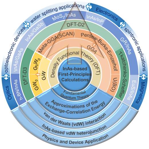
    Fig. 1. First-principles calculations theoretical framework and current research hotspots in InAs-based vdW heterojunctions
    (a)Crystal structure of bulk InAs[1]. Top and side view of geometric structures for(b-c)monolayer[62] and(d-e)bilayer[50] InAs with highlighted primitive unit cells
    Fig. 2. (a)Crystal structure of bulk InAs1. Top and side view of geometric structures for(b-c)monolayer62 and(d-e)bilayer50 InAs with highlighted primitive unit cells
    InAs-based vdW stacking configurations. From top to bottom and left to right are(a)InTS/GR and AsTS/GR vdW heterostructures[30];(b)InAs/GaSb-ABII and InAs/GaSb-AAII vdW heterostructures[34];(c)InAs/InP-AA vdW heterostructures[32];(d)InAs/GaSb-AB5,InAs/GaAs-BB3 and InAs/InP-BB5 vdW heterostructures[31];(e)InAs/PbTe vdW heterostructures[36];(f)InTS(111)/GR vdW heterostructures[28];(g)GR/InTS(111)and GR/AsTS(1¯1¯1¯)vdW heterostructures[27];(h)MoS2/InTS(111)and MoS2/AsTS(1¯1¯1¯)vdW heterostructures[27];(i)MoS2/InTS(111)and MoS2/AsTS(111)vdW heterostructures[35];(j)GR/InAs and h-BN/InAs vdW heterostructures[29];(k)EuS/InAs(001)-C1,EuS/InAs(001)-C3 and EuS/InAs(001)-C4 vdW heterostructures[33];(l)GR/InAs(110),GNR/InAs(110),GR/Au/InAs(110)and GNR/Au/InAs(110)vdW heterostructures[26]
    Fig. 3. InAs-based vdW stacking configurations. From top to bottom and left to right are(a)InTS/GR and AsTS/GR vdW heterostructures30;(b)InAs/GaSb-ABII and InAs/GaSb-AAII vdW heterostructures34;(c)InAs/InP-AA vdW heterostructures32;(d)InAs/GaSb-AB5,InAs/GaAs-BB3 and InAs/InP-BB5 vdW heterostructures31;(e)InAs/PbTe vdW heterostructures36;(f)InTS(111)/GR vdW heterostructures28;(g)GR/InTS(111)and GR/AsTS(1¯1¯1¯)vdW heterostructures27;(h)MoS2/InTS(111)and MoS2/AsTS(1¯1¯1¯)vdW heterostructures27;(i)MoS2/InTS(111)and MoS2/AsTS(111)vdW heterostructures35;(j)GR/InAs and h-BN/InAs vdW heterostructures29;(k)EuS/InAs(001)-C1,EuS/InAs(001)-C3 and EuS/InAs(001)-C4 vdW heterostructures33;(l)GR/InAs(110),GNR/InAs(110),GR/Au/InAs(110)and GNR/Au/InAs(110)vdW heterostructures26
    Interfacial charge transfer characteristics in InAs/GR vdW system.(a)InTS/GR vdW heterostructures,magenta and cyan represent the charge accumulation and depletion[30];(b)GR/Au/InAs vdW heterostructures[26];(c)InAs/GR vdW heterostructures,yellow and blue represent the charge accumulation and depletion[37];(d)InTS/GR vdW heterostructures,blue and red represent the charge accumulation and depletion[28];(e)GR/InAs vdW heterostructures,green and yellow represent the charge accumulation and depletion[27]
    Fig. 4. Interfacial charge transfer characteristics in InAs/GR vdW system.(a)InTS/GR vdW heterostructures,magenta and cyan represent the charge accumulation and depletion30;(b)GR/Au/InAs vdW heterostructures26;(c)InAs/GR vdW heterostructures,yellow and blue represent the charge accumulation and depletion37;(d)InTS/GR vdW heterostructures,blue and red represent the charge accumulation and depletion28;(e)GR/InAs vdW heterostructures,green and yellow represent the charge accumulation and depletion27
    Band structures for(a-b)GR/InAs[26,27],(c)h-BN/InAs[29],(d)EuS/InAs[33] and(e)InAs/PbTe[36] vdW heterostructures;DOS for(f)MoS2/InTS and(g)MoS2/AsTS vdW heterostructures[35]
    Fig. 5. Band structures for(a-b)GR/InAs2627,(c)h-BN/InAs29,(d)EuS/InAs33 and(e)InAs/PbTe36 vdW heterostructures;DOS for(f)MoS2/InTS and(g)MoS2/AsTS vdW heterostructures35
    (a)DOS for the composite vdW system with insertion of monolayer BN between InAs and metal(Pd and Pt)[37];(b)I-V characteristics of InAs/GR vdW heterostructure device[28];(c)Trends in band gap variation of InAs/GaSb vdW heterostructures under external electric field modulation[34];(d)The SBH(ϕp and ϕn)and band gap(ϕp + ϕn)of GR/InAs vdW heterostructures under external electric fields modulation[30]
    Fig. 6. (a)DOS for the composite vdW system with insertion of monolayer BN between InAs and metal(Pd and Pt)37;(b)I-V characteristics of InAs/GR vdW heterostructure device28;(c)Trends in band gap variation of InAs/GaSb vdW heterostructures under external electric field modulation34;(d)The SBH(ϕp and ϕn)and band gap(ϕp + ϕn)of GR/InAs vdW heterostructures under external electric fields modulation30
    Optical absorption coefficient of(a)InAs/GaAs-BB3 and(b)InAs/GaSb-AB5[31],(c)InAs/GaSb-ABII and InAs/GaSb-AAII[34],(d)MoS2/InAs[27],(e)InAs/InP[32] vdW heterostructures;(f)For InAs/GaAs and InAs/GaSb vdW heterostructures,the PCE can be as high as 20.65% and over 18%,respectively[31]
    Fig. 7. Optical absorption coefficient of(a)InAs/GaAs-BB3 and(b)InAs/GaSb-AB531,(c)InAs/GaSb-ABII and InAs/GaSb-AAII34,(d)MoS2/InAs27,(e)InAs/InP32 vdW heterostructures;(f)For InAs/GaAs and InAs/GaSb vdW heterostructures,the PCE can be as high as 20.65% and over 18%,respectively31
    (a)Spin density across EuS/InAs vdW heterogeneous interface[73];(b)Spin polarization as a function of layer index in EuS/InAs vdW heterostructure[33]
    Fig. 8. (a)Spin density across EuS/InAs vdW heterogeneous interface73;(b)Spin polarization as a function of layer index in EuS/InAs vdW heterostructure33
    Number of InAs layersEnergetically stable InAs-based vdW heterostructuresvdW correction functionalsExchange-correlation functionalsd(Å)ΔQ(e)Eg(eV)Ref.
    MonolayerInTS/GRDFT-D2HSE063.470+

    1.450i/ΓK

    1.500d/ΓΓ

    30
    AsTS/GRDFT-D2HSE063.500+

    1.340i/ΓK

    1.500d/ΓΓ

    30
    InAs/PbTeDFT-D3HSE063.46836
    InAs/InP-AADFT-D2HSE06+0.960i32
    InAs/InP-BB5DFT-D3HSE061.611i31
    InAs/GaAs-BB3DFT-D3HSE061.240i31
    InAs/GaSb-AB5DFT-D3HSE061.395i31
    InAs/GaSb-ABIIDFT-D33.738+0.1800.279i34
    InAs/GaSb-AAIIDFT-D33.876+0.1200.661d34
    BilayerGR/InAsDFT-D3Meta-GGA(SCAN)3.266+29
    h-BN/InAsDFT-D3Meta-GGA(SCAN)3.359+29
    MultilayerInTS(111)/GRDFT-D22.830-28
    GR/InTS(111)DFT-D22.820-1.91027
    GR/AsTS(1¯1¯1¯DFT-D23.310+0.29027
    GR/InAs(110)DFT-D23.200+0.01026
    GNR/InAs(110)DFT-D23.240+0.09626
    GR/Au/InAs(110)DFT-D23.080+0.01226
    GNR/Au/InAs(110)DFT-D22.560+0.08126
    MoS2/InTS(111)DFT-D22.640-2.06027
    MoS2/InTS(111)DFT-D22.720+0.50835
    MoS2/AsTS(111)DFT-D22.840-0.30535
    MoS2/AsTS(1¯1¯1¯DFT-D22.710-0.35027
    EuS/InAs(001)-C1T-SU(BO)2.600+33
    EuS/InAs(001)-C3T-SU(BO)2.400+33
    EuS/InAs(001)-C4T-SU(BO)2.600+33
    Table 1. Computational details (vdW correction functionals and exchange-correlation functionals where GGA-PBE is omitted). Computational results for structural parameters and electronic properties (interlayer distance d (Å), charge transfer ΔQ (e) and band gap Eg (eV)) of energetically stable InAs-based vdW heterojunctions. The plus sign indicates the charge transfer from 2D layered materials to InAs materials, and the minus sign is the opposite. The upper labels i and d indicate the indirect and direct band gap, respectively.
    Tian-Tian CHENG, Kun ZHANG, Man LUO, Yu-Xin MENG, Yuan-Ze ZU, Yi-Jin WANG, Peng WANG, Chen-Hui YU. Research progress on first-principles calculations of interfacial charge transfer characteristics in InAs-based van der Waals heterojunctions[J]. Journal of Infrared and Millimeter Waves, 2023, 42(5): 666
    Download Citation