Tian-Tian CHENG, Kun ZHANG, Man LUO, Yu-Xin MENG, Yuan-Ze ZU, Yi-Jin WANG, Peng WANG, Chen-Hui YU. Research progress on first-principles calculations of interfacial charge transfer characteristics in InAs-based van der Waals heterojunctions[J]. Journal of Infrared and Millimeter Waves, 2023, 42(5): 666
Copy Citation Text
Vertical van der Waals heterostructures stacked by low-dimensional InAs materials and other two-dimensional layered materials have been widely applied in emerging fields such as nanoelectronics, optoelectronics, and quantum information. To comprehend their extraordinary device performance, it is crucial to explore the charge transfer mechanism across the junction interface. First-principles calculations play an indispensable role in revealing the intrinsic relationship between interfacial charge transfer characteristics and electrical, optical, and magnetic principle physical properties as well as device performance variations in various energetically stable InAs-based van der Waals heterojunctions. Recent theoretical research on interfacial charge transfer characteristics in InAs-based van der Waals heterostructures, as well as their potential for functional applications are combed, summarized, and discussed. Several avenues are proposed for the potent development of first-principles calculations in terms of theoretical methodology and calculation accuracy, providing a basis for quantitative research that can be leveraged to propel fundamental scientific studies and applied device designs of InAs-based van der Waals heterojunctions.
InAs is renowned for narrow direct band gap,high electron mobility,and excellent photoresponse[1-3]. Layer-by-layer stacked InAs-based van der Waals(vdW)heterostructures have drawn considerable interest among researchers,triggering further innovative physics and functional devices[4-6]. Not only do they preserve the desirable properties of individual components,but they also display distinctive electrical,optical,magnetic properties and device performance variations arising from interfacial charge transfer. Comprehending the intricate interfacial charge transfer mechanism is the cornerstone in elucidating the root causes of diverse principle physical properties and novel device mechanisms[7-12]. This holds the key to unleashing the full potential of InAs-based vdW heterostructures and devices,providing great promise for the advancement of ultrafast electronics and optoelectronics[13-17].
However,it is insufficient to perform systematic research on InAs-based vdW heterojunctions solely through experimentation. One major obstacle is the absence of perfect InAs-based vdW heterostructures,considering that completely flawless monolayer or bilayer InAs have not yet been fabricated in experiments. An additional ongoing problem is that traditional experimental methods often encounter limitations when it comes to considering defects on material surfaces or heterogeneous interfaces at the atomic and electronic levels[18,19]. In light of the challenges mentioned above,the necessity and significance of first-principles calculations(FPC)become increasingly prominent. Complementary to experiments,theoretical calculations offer an essential and valuable approach to exploring unknown InAs vdW materials and gaining insight into the unique principle physical properties and device mechanisms in InAs-based vdW heterojunctions.
There is no denying that vdW interactions related to heterogeneous interface configurations play a vital role in determining physical properties and device performance in vdW heterojunctions. Inspiringly,feasible,and reliable vdW models in FPC such as DFT-D[20-23] and Tkatchenko-Scheffler(T-S)[24],provide exciting opportunities for comprehensive and in-depth research in materials science and condensed matter physics[18,25]. Particularly,the application of vdW models to InAs vdW systems represents a highly active and important research area. The successful evaluation of long-range,weak vdW interactions between InAs and adjacent heteromolecular layers provides theoretical guidance and accurate prediction for intriguing principle physical properties and device performance variations in InAs-based vdW heterojunctions. Furthermore,they offer promising opportunities for the development of high-quality InAs-based vdW heterojunction devices,opening up new avenues for basic science research and applied device design.
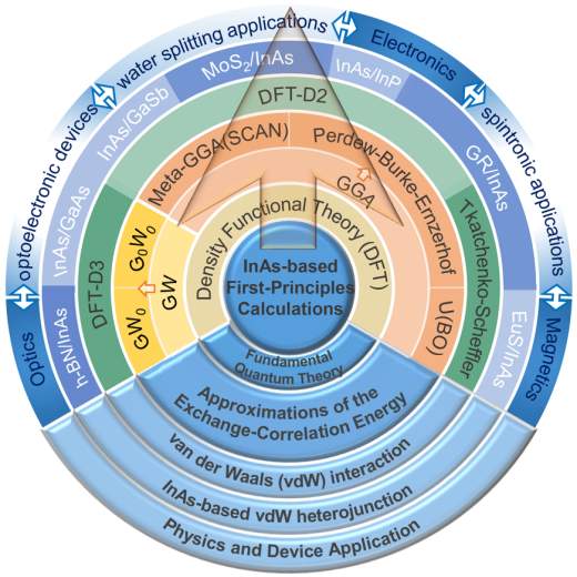
This review presents the theoretical framework for recent research on InAs-based vdW heterojunctions using FPC,which focuses on exploring the interfacial charge transfer characteristics across InAs-based vdW heterojunctions and their impact on the principle physical properties and novel device mechanisms. As depicted in Fig. 1,FPC have conducted multi-level,critical,and prospective research in InAs-based vdW heterojunctions[26-37]. Plenty of basic theory and computational methods are first introduced and compared. Numerous energetically stable InAs-based vdW heterostructure models screened out by FPC are then summarized. Subsequently,various methods have been proposed to quantify interfacial charge transfer characteristics. This provides a thorough grasp of the relationship between interfacial charge transfer mechanism and unique principle physical properties as well as device performance variations in InAs vdW systems,including band engineering and orbital hybridization,interacting with external electric fields,enhanced optical absorption,and proximity-induced magnetism. Moreover,FPC have been employed to extract several other crucial parameters,such as the effective mass,carrier mobility,and work function[27,31,32,35]. However,these results receive relatively less attention because they have gone too far beyond available experimental verifications. Finally,in order to continue to play an irreplaceable guiding and forecasting role in the research of the InAs vdW system,several avenues are tentatively proposed that FPC should be vigorously developed from both theoretical methodology and calculation accuracy. Overall,this review systematically summarizes and discusses the interfacial charge transfer characteristics in InAs-based vdW heterojunctions,paving the way for innovative InAs-based vdW heterojunction devices in electronics,optics,and magnetics.
Figure 1.First-principles calculations theoretical framework and current research hotspots in InAs-based vdW heterojunctions
FPC is a powerful computational method based on the basic laws of quantum mechanics. Using well-defined physical constants as inputs,it solves the Schrödinger equations through a series of approximations and simplifications,providing significant insights into the fundamental causes of semiconductor material properties and device performance[18,25,38-40]. This section introduces basic theory and computational methods,which are employed to predict the interface charge transfer dynamics in InAs-based vdW heterojunctions. It encompasses density functional theory(DFT)and various exchange-correlation functionals,including local density approximation(LDA),generalized gradient approximation(GGA),GW approximation,hybrid functionals,as well as vdW models. By evaluating the advantages and limitations,the most appropriate computational model can be identified for research on the InAs vdW system,enhancing the precision and accuracy of the computational results.
1.1 DFT
DFT has emerged as the preeminent method for computing semiconductor material properties in materials science and condensed matter physics[25,38]. In almost all DFT calculations,the Kohn-Sham scheme is utilized to determine both the ground-state electron density and the corresponding total energy[41,42]. The Kohn-Sham equations are often solved through the plane-wave basis set along with the projector augmented-wave method,which has been implemented in the Vienna Ab initio Simulation Package[18,40].
1.2 LDA, GGA, and GW approximation
The accuracy and precision of DFT are significantly influenced by exchange-correlation functionals. In order of increasing complexity,LDA,GGA,and meta-GGA are presented. Of these,the Perdew-Burke-Ernzerhof GGA(GGA-PBE)exchange-correlation energy functional has been extensively employed in the analysis of both molecular and extended systems[43]. Additionally,GW approximation offers quasiparticle energies values based on non-local and dynamic electron-electron interaction within many-body perturbation theory[44].
1.3 Hybrid functionals
Hybrid functionals,such as Heyd-Scuseria-Ernzerhof(HSE06),have been demonstrated to possess remarkable accuracy in predicting electronic structure,band gaps,and magnetic moments and so on. Outstanding predictive capability arises from the partial incorporation of the exact exchange energy derived from the Hartree-Fock theory into the semi-local DFT exchange-correlation energy[19,25].
1.4 vdW models
Following the discussion of basic theory and exchange-correlation energy functionals in FPC,vdW models based on paired vdW potentials are introduced. Traditional LDA and GGA frequently ignore the long-range,non-local correlation vdW interactions[45],whereas the semi-empirical long-range dispersion correction DFT-D series approaches[20-23] and the pairwise dispersion T-S method[24] have widely succeeded in describing vdW interactions. These vdW models require the specification of two parameters:dispersion coefficients C6 and cutoff radii[39],providing an effective pathway for understanding and predicting the interface charge transfer dynamics in InAs-based vdW heterojunctions.
1.5 Reproducibility in first-principles calculations
The widespread use of FPC has resulted in the development of numerous software and codes,each with its unique formalism. However,the common software and codes are capable of performing primary or advanced DFT and generating fundamentally consistent results[40,46]. The feasibility and reproducibility in theoretical calculation are crucial for achieving meaningful comparisons between theoretical outcomes and experimental results,which drives scientific research of InAs-based vdW heterostructures and device applications.
1.6 Computational details in InAs-based vdW heterojunctions
To determine the optimal computational model,we conduct a meticulous comparison and analysis among computational details in InAs-based vdW heterojunctions,taking into account various factors such as accuracy,efficiency,and feasibility. The primary objective is to offer a valuable reference for future research endeavors on theoretical research in InAs-based vdW heterojunctions.
Conducting FPC to explore the electronic band structure,alongside the size and type of the band gap,is indispensable for acquiring a comprehensive understanding of the fundamental physical properties and device mechanisms in InAs vdW systems. From both theoretical and empirical observations of FPC,LDA and GGA tend to underestimate the actual band gap values of monolayer or bilayer InAs to some extent due to self-interaction[30-32,34,47-49]. While the strongly constrained and appropriately normed(SCAN)meta-GGA has demonstrated improved band gap predictions,it still exhibits underestimation in numerous scenarios[29,50]. Hybrid functionals and GW approximation have proven effective in mitigating the underestimation of band gaps caused by semi-local exchange-correlation functionals[44]. In contrast,HSE06[30-32,51] has yielded more precise predictions whereas GW0[47]and G0W0[48]calculations have slightly overestimated values.
In the case of InAs multilayers,sheets,or slabs,the band gaps calculated by Bayesian optimization U(BO)calculations decrease as the number of layers increases and eventually approach the bulk gap value of about 0.35 eV,signifying a layer-dependent characteristic[33,52]. Further,the band gap type for InAs exhibit similar dependency on computational methods,with some studies claiming that it is direct while others argue it is indirect,reflecting the complexity and uncertainty of electronic structure calculations[31,32,48]. In contrast,it is evident that even primary DFT calculation can reproduce nearly the same lattice constants around 0.43 nm for InAs within errors of a few percent,reaching a satisfactory agreement[18,53,54]. Thus,it is significant to choose the appropriate computational method for accurately estimating principle physical properties and device performance variations in InAs-based vdW heterojunctions.
Importantly,it is crucial to consider the long-range weak vdW interactions when performing FPC in InAs-based vdW heterojunctions[55,56]. Over time,DFT-D approaches have been continually refined,leading to increased accuracy and decreased reliance on empiricism. For instance,the semi-empirical DFT-D2 method has succeeded in describing vdW interactions across InAs vdW heterojunctions,yielding satisfactory theoretical results[26-28,30,32,35]. In the current research,a refined version of DFT-D3 has been employed due to higher accuracy,reduced empiricism,and wider applicability[29,31,34]. Alternatively,the parameter-free and nonempirical T-S method provide comparable results in describing the vdW interactions across InAs vdW heterojunctions[33]. Future research should continue to concentrate on refining the underlying theory and developing computational tools to gain a better understanding of the influence of weak vdW interactions on InAs-based vdW heterojunctions.
2 InAs-based vdW heterostructure models
Recently,low-dimensional InAs-based materials have gained significant attention in the research community. Monolayer or bilayer InAs,as well as various stable InAs-based vdW heterostructures,have been obtained through energy minimization and geometrical optimization by FPC. Remarkably,the stability of these vdW heterostructures is highly influenced by variables related to interfacial vdW interactions. These findings respect a significant breakthrough in exploring abundant InAs-based vdW heterojunctions,paving the way for potential functional applications in InAs-based vdW heterostructures,leading to significant technological advancements in the future.
2.1 Low-dimensional InAs-based materials
Fig. 2(a)illustrates crystal structure of bulk InAs,where the covalent radii of In and As atoms are 1.44 Å and 1.2 Å,respectively[1,35]. Each In anion exhibits hexagonal coordination with four neighboring As cations while the As anions coordinate with the four In cations,creating the tetrahedral bonding environment. The nonlayered structure poses a significant challenge in the synthesis of ultra-thin InAs films. Recently,the study of low-dimensional emerging semiconductor materials with honeycomb structures,such as graphene(GR),and hexagonal boron nitride,has revealed a wealth of exciting physical and chemical properties[57-60]. Motivated by these works,Şahin et al. first examined the possibility of the existence of two-dimensional(2D)hexagonal monolayer InAs using DFT within FPC[47]. The comparative analysis of the total energy,phonon modes,and electronic structures indicates that monolayer InAs prefer to adopt low-buckled(BK)hexagonal structure rather than hexagonal planar(PL)structure like GR,as depicted in Fig. 2(b-c). Non-planar structures can be traced back to the formation of sp3-like orbitals,which is attributed to the weakening of the π-bonds. Further theoretical studies have confirmed these findings and proposed additional potential stable 2D monolayer InAs structures,including 2D tetragonal[48],hexagonal zigzag[61],and hexagonal armchair[62].
Figure 2.(a)Crystal structure of bulk InAs[1]. Top and side view of geometric structures for(b-c)monolayer[62] and(d-e)bilayer[50] InAs with highlighted primitive unit cells
Excitingly,Lucking et al. have recently predicted that InAs can exist in a stable layered form[63]. In the ultrathin limit,the double layer honeycomb(DLHC)InAs is more energetically favorable than the single layer honeycomb(SLHC)or truncated bulk(BT)InAs associated with the three-dimensional bulk phase,as demonstrated in Fig. 2(d-e)[50,64]. All cations in DLHC InAs are structurally bound to three anions from the same layer and one anion from another layer,forming a distorted tetrahedral coordination. Notably,within the thickness range of 3-12 monolayers,the truncated haeckelite structure is considered to be energetically favorable,which is characterized by the presence of alternating octagonal and square rings[65]. Until now,the fabrication of pure InAs vdW materials remains unattainable in experiments,no matter what type of geometry they belong to. Nevertheless,considering that the calculated formation energy of monolayer and bilayer InAs can be comparable to existing materials with similar bulk structures[66,67],researchers keep an optimistic attitude and are working to make leaps in experimental preparation technology. High reward of experimental insistence in this respect is mostly probable since monolayer and bilayer InAs as fundamental building blocks can open new avenues for both perfect and hybrid vdW integrations.
2.2 InAs-based vdW stacking configurations
Various InAs-based vdW heterostructures have been constructed with optimized InAs geometric structures above as the base unit. Undoubtedly,to fully harness the potential of InAs-based vdW heterojunctions,it is imperative to comprehend structural stability,as well as the thermodynamic stability when defects present at the heterogeneous interface. Computational details and results are presented in Table 1. Notably,GGA-PBE has been taken into consideration for all situations,which is no longer specifically emphasized in the exchange-correlation energy functionals. The system energy is generally expressed in terms of the total energy and its derivative energies[39],such as cohesive energy[31],binding energy[27-29,32,34],adsorption energy[26],or formation energy[35]. The following equation gives the total energy adjusted by dispersion with DFT-D[21]:
,
where Etot,EKS-DFT,and Edisp represent the total energy of the InAs-based vdW system,the conventional self-consistent Kohn-Sham energy obtained from exchange-correlation energy functionals,and the contribution of the dispersion correction by DFT-D.
Table 1. Computational details (vdW correction functionals and exchange-correlation functionals where GGA-PBE is omitted). Computational results for structural parameters and electronic properties (interlayer distance d (Å), charge transfer ΔQ (e) and band gap Eg (eV)) of energetically stable InAs-based vdW heterojunctions. The plus sign indicates the charge transfer from 2D layered materials to InAs materials, and the minus sign is the opposite. The upper labels i and d indicate the indirect and direct band gap, respectively.
So far,theoretical exploration has screened quite a few energetically stable InAs-based vdW heterostructures as depicted in Fig. 3,predicting the feasibility of experimental preparation. Part of them are stacking configurations with as-yet-unverified InAs monolayer,including InAs/GR[30],InAs/GaSb[31,34],InAs/GaAs[31],InAs/InP[31,32],and InAs/PbTe[36]. The rest are vertical combinations with InAs multilayer,slabs or sheets,covering GR/InAs[26-29],GR/Au/InAs[26],MoS2/InAs[27,35],h-BN/InAs[29],and EuS/InAs[33]. Significantly,within the GR/InAs vdW heterostructures,In atoms energetically favor occupying the H-site located at the center of the carbon honeycomb lattice[60,68,69]. It is well established that variables related to interfacial vdW interactions significantly affect system energy,including stacking configuration,interlayer spacing,crystal orientation,lattice constant,surface polarity,and surface atom termination[27,31,33-35]. To be specific,featuring low-buckling,InAs exhibit two polar terminated surfaces,either In-terminated InAs surface(InTS)or As-terminated InAs surface(AsTS)[27,35,70]. Consistently,InTS is demonstrated to be more energetically stable than AsTS in both GR/InAs and MoS2/InAs vdW heterostructures,where the larger In atoms result in significantly shorter interlayer spacing and stronger interfacial interaction. These findings shed new insights into InAs-based vdW heterostructures,highlighting the significant role of critical variables associated with interfacial vdW interactions in determining system stability.
Figure 3.InAs-based vdW stacking configurations. From top to bottom and left to right are(a)InTS/GR and AsTS/GR vdW heterostructures[30];(b)InAs/GaSb-ABII and InAs/GaSb-AAII vdW heterostructures[34];(c)InAs/InP-AA vdW heterostructures[32];(d)InAs/GaSb-AB5,InAs/GaAs-BB3 and InAs/InP-BB5 vdW heterostructures[31];(e)InAs/PbTe vdW heterostructures[36];(f)InTS(111)/GR vdW heterostructures[28];(g)GR/InTS(111)and GR/AsTS()vdW heterostructures[27];(h)MoS2/InTS(111)and MoS2/AsTS()vdW heterostructures[27];(i)MoS2/InTS(111)and MoS2/AsTS(111)vdW heterostructures[35];(j)GR/InAs and h-BN/InAs vdW heterostructures[29];(k)EuS/InAs(001)-C1,EuS/InAs(001)-C3 and EuS/InAs(001)-C4 vdW heterostructures[33];(l)GR/InAs(110),GNR/InAs(110),GR/Au/InAs(110)and GNR/Au/InAs(110)vdW heterostructures[26]
While ideal interfaces serve as an important benchmark,defects exist on real material surfaces or heterogeneous interfaces,which will seriously affect the device performance. Thus,it is necessary to take defects into account when assessing the stability of InAs-based vdW heterostructures. Calculations have demonstrated that the formation of In and As vacancies at the interface of InAs-based vdW heterostructures is accompanied by either absorption or exothermic exchange processes,and also causes disturbance to system stability[35,71]. In reality,the situation may be more complex than what can be predicted by simple calculations. Additional factors,such as temperature and strain,may also have a considerable impact on the formation of defects,which ultimately affect the stability of InAs-based vdW heterostructures to a certain extent. Therefore,additional research is necessary to thoroughly characterize the impact of these factors on the stability of the InAs vdW system,aiming to develop more durable and dependable InAs-based vdW heterogeneous interfaces.
Overall,theoretical exploration has identified the existence of InAs vdW materials,including monolayer InAs,bilayer InAs,and InAs-based vdW heterojunctions. The stability of InAs-based vdW heterostructures is significantly influenced by interfacial vdW interactions,which can be affected by multiple factors such as stacking configuration,interlayer spacing,crystal orientation,and surface atom termination. Furthermore,it is essential to consider defects in vdW heterogeneous interface when assessing the structural stability. Therefore,it is necessary to thoroughly characterize the impact of these factors on the stability of InAs vdW systems. These findings not only advance understanding of the fundamental properties of InAs-based vdW heterojunctions but also provides a valuable guideline for the continued development of emerging InAs vdW systems.
3 Physics and functional devices
The interfacial charge transfer characteristics in InAs-based vdW heterojunctions have been the subject of intense research. Various analytical methods have been proposed to evaluate interfacial charge transfer mechanism,including energy band structure,the density of states(DOS),Bader and Mulliken analyses. While energy band structure and DOS provide insightful information,Bader and Mulliken analyses offer precise and quantitative data. Furthermore,charge density difference(CDD)visualization provides a clear representation of the direction and quantity of interfacial charge transfer. Remarkably,it has been discovered that changes in the interlayer spacing of InAs-based vdW heterojunctions can modify the strength of the vdW force,which is the primary cause for the changes in the direction and extent of interfacial charge transfer. These recent findings offer valuable insights into the fundamental physics underlying the electrical,optical,and magnetic properties,as well as the device performance variations in InAs-based vdW heterojunctions.
FPC have provided insight into the performance evaluation and scenarios of InAs-based vdW heterojunctions in important functional applications. These heterojunctions exhibit remarkable potential for band engineering,including band gap opening,band inversion,and band dispersion. Moreover,FPC have investigated the role of orbital hybridization in modifying the electronic properties of these heterostructures. Furthermore,the interfacial charge transfer and the subsequent built-in electric field at the heterogeneous interface are vital to achieving outstanding performance. The electronic transport properties can be further modulated by external electric fields. Excitingly,theoretical investigations have emphasized that interfacial charge transfer is the crucial driving force behind efficient optical absorption and photoresponse in InAs-based vdW heterojunctions. Lastly,FPC have demonstrated the existence of proximity-induced magnetism in InAs-based vdW heterojunctions,though the magnetic moments generated in the InAs layer are highly localized and too weak to be practical. These findings contribute significantly to the increasing knowledge base on the physics and applications of vdW heterojunctions,opening up exciting prospects for further research in this area.
3.1 Interfacial charge transfer quantification
To comprehend the distinctive physical characteristics of InAs-based vdW heterojunctions,it is imperative to gain a comprehensive understanding of the interfacial charge transfer parameters,which include the direction and quantity of charge transferred. Along with band structure and DOS,Bader and Mulliken analyses combined with CDD offer a powerful tool for investigating the properties of interfacial charge transfer. Our analysis underscores the importance of vdW forces in interfacial charge transfer,highlighting the potential of interlayer spacing as a general tuning parameter for vdW heterojunctions. These insights can enable researchers to explore the unique properties of InAs-based vdW heterojunctions and unlock their full potential for diverse applications.
Band structure and DOS offer valuable insight into the interfacial charge transfer properties of InAs-based vdW heterojunctions. The charge transfer,as well as well-separated electron-hole pairs at the interfaces of InAs-based vdW heterojunctions,can be induced by various factors,such as differences in work functions,ionizations,and nucleophilics[38]. The redistribution and transfer of charges at the interface can be elucidated through an analysis of the work function and Fermi energy level. It is important to note that the interface reconstruction has an impact on the work function of InAs-based vdW heterostructures. The computed work function may differ slightly,as identical components in different heterostructures may exhibit differences after optimization[27]. Therefore,a comprehensive approach is needed for accurate modeling and prediction when designing and analyzing InAs-based vdW heterostructures.
To achieve a more quantitative understanding of the interfacial charge transfer in InAs-based vdW heterojunctions,Bader analyses[27] and Mulliken analyses[30,34] have been employed. Computational results have been presented in Table 1. By maintaining the total electron density,Bader analysis provides a reliable means for characterizing the charge distribution. As a result,it has become a preferred approach for researchers seeking to understand the electronic properties of materials and molecules[72]. A comprehensive understanding of the charge transfer process can be obtained by evaluating the changes in charge density before and after the charge transfer[27]:
,
where ρvdWH,ρInAs, and ρm are the charge density of the InAs-based vdW heterostructures,isolated InAs,and other 2D layered materials subsystems,respectively. The planar average CDD along the z-direction(perpendicular to the interface)is:
,
where Axy is the surface unit cell. The corresponding three-dimensional isosurfaces of the CDD visually depict the spatial distribution and extent of charge accumulation and depletion at the heterojunction interface. This information sheds valuable insight into the interfacial charge transfer parameters and their consequences on unique properties and device performance of InAs-based vdW heterojunctions.
The charge density difference consistently indicates that the maximum charge transfer occurs near the heterojunction interface. Surprisingly,there are intriguing differences in the transfer direction and quantity of interfacial charge in GR/InAs vdW system. In terms of different GR/InAs vdW heterostructures,the charge from GR to InAs layer in Fig. 4(a-b)[26,30,69],while the InAs layer lose charge in Fig. 4(c-d)[28,37]. Amazingly,Fig. 4(e)illustrates that the direction of charge transfer in the GR/InTS vdW heterostructures is opposite to that in the GR/AsTS vdW heterostructures,with a more intense interfacial charge transfer in the former[27]. Upon conducting a comprehensive analysis,we infer that the alteration of interlayer spacing serves as the main driving factor for the changes in both the direction and quantity of charge transfer. This is due to the modification in the strength of the vdW force resulting from the change in interlayer spacing. The vdW interactions stem from the intricate electronic correlations that result in a net attraction between electron fragments within a multi-electron system,which are crucial for facilitating charge transfer. The interlayer distance may be successfully tuned by altering several variables related to interfacial structure,such as crystal orientation,surface atom termination,film thickness,and external stress[31,34]. Such tuning can lead to substantial changes in the direction and extent of interfacial charge transfer in InAs-based vdW heterojunctions. Our findings shed new light on the mechanism of interfacial charge transfer in InAs-based vdW heterojunctions and contribute to an in-depth understanding of physical principles of intriguing electricity,optics,and magnetism properties as well as device performance variations in InAs-based vdW heterojunctions.
Figure 4.Interfacial charge transfer characteristics in InAs/GR vdW system.(a)InTS/GR vdW heterostructures,magenta and cyan represent the charge accumulation and depletion[30];(b)GR/Au/InAs vdW heterostructures[26];(c)InAs/GR vdW heterostructures,yellow and blue represent the charge accumulation and depletion[37];(d)InTS/GR vdW heterostructures,blue and red represent the charge accumulation and depletion[28];(e)GR/InAs vdW heterostructures,green and yellow represent the charge accumulation and depletion[27]
Interfacial charge transfer is a critical phenomenon that has attracted significant research interest due to its potential to modify the electronic properties of heterojunctions. Recent investigations have demonstrated that interfacial charge transfer plays a pivotal role in band engineering of InAs-based vdW heterojunctions. Notably,the electronic orbital hybridization between adjacent interfacial atoms largely affects the band gap of InAs vdW systems. Moreover,the design of vacancy defects offers new prospects for band gap engineering. These findings are of particular importance for the design and optimization of electronic and optoelectronic devices based on InAs-based vdW heterojunctions.
Interfacial charge transfer characteristics influence electron band structures of InAs-based vdW heterojunctions. Fig. 5(a-b)shows that band gap of about 10 meV for GR in the GR/InAs vdW heterojunctions has been opened,offering a viable method to tune the semiconductor properties of GR[26,27]. As shown in Fig. 5(c),band inversion takes place in DLHC-InAs for h-BN/InAs vdW heterostructures,which is a novel phenomenon worthy of further study[29]. Furthermore,dispersed states appear at the InAs valence band maximum(VBM)in the EuS/InAs vdW heterostructures in Fig. 5(d),which is assumed to be connected to the charge transfer at the interface between EuS and InAs[33]. Rarely,experimental measurements have confirmed the existence of unique energy band structures[73]. For InAs/PbTe vdW heterostructures,the projected band structure in Fig. 5(e)demonstrates that the conduction band minimum(CBM)and the VBM are localized in different layers of the vdW heterostructure,indicating efficient electron-hole separation rate[36]. However,considering the complex nature of interfacial charge transfer,it is crucial to conduct both experimental and theoretical investigations of different InAs-based vdW heterojunctions to further validate these findings. This will advance our understanding of these materials and pave the way for a range of technological applications.
Surprisingly,the band gap of the InAs vdW system is not solely determined by the constituent thin films,as may be expected. Rather,it is influenced to a greater extent by the electronic orbital hybridization that occurs between the adjacent interfacial atoms. Orbital hybridization between adjacent interfacial atoms plays a crucial role in facilitating the transfer of outer orbital electrons from one side of the interface to the vacant state on the other side of the interface,reducing the system energy to a lower steady state[35]. Fig. 5(f-g)show the DOS for MoS2/InTS and MoS2/AsTS vdW heterostructures,providing valuable insights into the nature of the orbital hybridization at the interface. Specifically,in the MoS2/InAs vdW heterostructure,valence electron orbitals are filled with Asp,Inp,Sp, and Mod electrons. The conduction band is primarily composed of Mod and Sp orbitals,while the valence band is primarily composed of Inp and Asp orbitals. However,hybridization is observed between Mod,Sp,Inp,and Asp orbitals in the vicinity of the Fermi energy level as a result of the interfacial interactions between the two materials. The MoS2/InTS and MoS2/AsTS vdW heterostructures result in n-type and p-type semiconductors,respectively. Remarkably,in non-ideal systems,the DOS is somewhat altered due to changes in the interfacial structure containing vacancy defects. In particular,interfacial In vacancies in MoS2/AsTS vdW heterostructures were found to reduce the band gap,while interfacial As vacancies caused the band gap to increase. These findings open up the intriguing option of band gap tuning via vacancy defects,opening up fresh possibilities for the creation of novel InAs-based vdW heterostructures with tailored functionalities.
To sum up,interfacial charge transfer plays a crucial role in the electron band structure of InAs-based vdW heterojunctions. Theoretical studies reveal the emergence of band engineering such as band gap opening,band inversion,and band dispersion,as well as the role of orbital hybridization in promoting electron transfer in outer orbitals. Additionally,the study highlights the potential of band gap tuning via vacancy defects in non-ideal systems. However,there is still a lack of knowledge in this field,and future research should focus on exploring the properties and functionalities of various InAs-based vdW heterostructures and understanding the fundamental mechanisms behind interfacial charge transfer and band engineering as well as orbital hybridization.
3.3 Interacting with external electric fields
The formation of a built-in electric field at the interface of InAs-based vdW heterostructures induces changes in the conduction type of the interfacial atomic layer,thereby presenting a promising new doping approach. Moreover,the electronic structure and transport properties of InAs-based vdW heterojunctions can be controlled by applying a vertical external electric field. InAs-based vdW heterojunctions exhibit flexible electronic properties under external electric fields,which have crucial applications in next-generation electronic devices.
The formation of a built-in electric field at the interface of InAs-based vdW heterostructures is attributed to charge transfer between the materials. The quantity of the built-in electric field increases proportionally with the quantity of charge transferred until it reaches equilibrium with the intrinsic polarization electric field at the surface of the InAs film. This charge transfer effect induces changes in the conduction type of the interfacial atomic layer,leading to a novel doping approach for 2D layered materials associated with InAs-based vdW heterostructures. This doping technique outperforms conventional methods,such as impurity doping,which typically increases phonon scattering and electronic impurities[27,28].
The application of a vertical external electric field can induce a redistribution of charge between the layers in InAs-based vdW heterojunctions[72]. When the applied electric field is in the opposite direction to the built-in electric field,the motion of the electrons is restarted. Conversely,the motion of the electrons is further inhibited. This presents a feasible method for modulating the electronic structure and transport properties of InAs-based vdW heterojunctions. The direction of electron transport through the interface is determined by the interface polarization and electrostatic potential energy,while the contact barrier height affects the intensity of the current,and the interface charge distribution affects tunneling transmission probability[28].
Recent computational studies have highlighted the flexible electron transport properties in InAs-based vdW heterojunctions. For instance,creating vdW heterojunction by inserting BN reduces the electronic states near the Fermi level of InAs with Pt and Pd electrode interfaces in Fig. 6(a)[37]. Moreover,2D InAs achieve p-type ohmic contact with the Pt electrode. Single-gated InAs/GR heterostructure device exhibits rectification behavior and negative differential resistance effect without gate voltage in Fig. 6(b)[28]. In addition,Fig. 6(c-d)demonstrates that tunable band gap size and vdW contact type have happened to InAs/GaSb and GR/InAs vdW heterostructures under external electric fields,respectively[30,34]. These excellent electronic properties are indispensable for junction-type and power devices. In summary,the application of external electric fields is a promising method for modulating the electronic structure and transport properties of InAs-based vdW heterojunctions. Future research directions may include exploring new material combinations for InAs-based vdW heterojunctions,developing new techniques for precise control of interface properties,and investigating the impact of environmental factors on device performance.
Figure 6.(a)DOS for the composite vdW system with insertion of monolayer BN between InAs and metal(Pd and Pt)[37];(b)I-V characteristics of InAs/GR vdW heterostructure device[28];(c)Trends in band gap variation of InAs/GaSb vdW heterostructures under external electric field modulation[34];(d)The SBH(ϕp and ϕn)and band gap(ϕp + ϕn)of GR/InAs vdW heterostructures under external electric fields modulation[30]
The construction of InAs-based vdW heterostructures represents a highly effective approach for enhancing the optical absorption performance beyond that of isolated constituent films. Theoretical investigations have emphasized the critical role of interfacial charge transfer in driving efficient optical absorption and photoreaction effects. These findings hold great potential for the development of novel optoelectronic devices with enhanced performance and efficiency.
The accurate analysis of optical absorption spectra in materials using FPC requires careful consideration of excitonic effects,electron-hole coupling,and phonon-assisted electron transitions[38]. InAs is known to exhibit high photoresponse,which can be attributed to ultrathin properties and high carrier mobility. These properties lead to a shorter migration distance between photogenerated electrons and holes,slowing down the electron-hole recombination. As shown in Fig. 7(a-e),InAs/GaAs,InAs/GaSb,MoS2/InAs and InAs/InP vdW heterostructures exhibit enhanced optical properties with a wider absorption range and stronger absorption coefficients compared to the corresponding single components[27,31,32,34]. Specifically,the InAs/GaSb vdW heterostructures exhibit improved optical absorption in the ultraviolet region[34]. InAs/GaAs vdW heterojunction solar cells have demonstrated a remarkable power conversion efficiency(PCE)of up to 20.65% in Fig. 7(f)[31]. The type-II energy band effectively suppresses excited holes and electrons in valence and conduction bands,promoting the full dissociation of photogenerated holes and electrons. However,InAs/InP vdW heterostructures are at a disadvantage compared to GaP/GaAs vdW heterostructures in water splitting applications[32]. Because the overlapping of InAs/InP vdW heterojunctions band structure at the interface is more violent,which is not conducive to inhibiting the recombination of photogenerated carriers. In general,the construction of InAs-based vdW heterostructures is an effective method for improving optical absorption performance,holding great potential for the experimental fabrication and testing of promising optoelectronic devices.
Figure 7.Optical absorption coefficient of(a)InAs/GaAs-BB3 and(b)InAs/GaSb-AB5[31],(c)InAs/GaSb-ABII and InAs/GaSb-AAII[34],(d)MoS2/InAs[27],(e)InAs/InP[32] vdW heterostructures;(f)For InAs/GaAs and InAs/GaSb vdW heterostructures,the PCE can be as high as 20.65% and over 18%,respectively[31]
Theoretical calculations reveal the intrinsic mechanism behind the efficient optical absorption and photoreaction in InAs-based vdW heterostructures,with an emphasis on the important role of interfacial charge transfer. In the GR/InTS vdW heterostructures,visible light irradiation induces the excitation of electrons on the pz orbitals of GR to the s and p orbitals in the conduction band of the InTS substrate[27]. The resulting optical absorption is significantly enhanced due to the strong orbital overlap and electron transition. Furthermore,substituting GR with MoS2 can further improve the optical absorption coefficient of the heterostructure in the visible to the near-infrared optical band. This is primarily due to the large interfacial charge transfer in the MoS2/InAs vdW heterostructure,which generates additional electron-hole pairs. These findings contribute to the fundamental understanding of the optical absorption mechanism in InAs-based heterostructures,underscoring the critical role of electronic transitions between occupied and non-occupied states in photoelectron interactions in determining the optical absorption mechanism of vdW heterostructures.
Overall,InAs-based vdW heterostructures holds immense potential for the development of advanced optoelectronic devices,including photodetectors,solar cells,and terahertz detectors,due to their excellent optical properties. Theoretical calculations have elucidated that the enhanced optical absorption is due to electronic transitions that occur at the junction interfaces. Despite the significant progress,there are still some limitations and challenges that need to be addressed in future research. For example,experimental validation of the theoretical predictions and the optimization of the heterostructure design to improve charge separation and reduce recombination losses are important future directions. Moreover,investigating the potential applications of these heterostructures in optoelectronic and energy conversion devices is an exciting avenue for future research.
3.5 Proximity-induced magnetism
In magnetics,EuS/InAs vdW heterostructures have attracted substantial attention for their tunable electronic transport and local proximitized magnetic exchange. However,neutron and x-ray reflectivity measurements have failed to detect proximity-induced magnetism in InAs. In contrast,FPC have proven to be a powerful tool for elucidating magnetic moment distribution at the EuS/InAs vdW heterogeneous interface[33,73]. The outcomes unequivocally demonstrate the feasibility of spin injection into the InAs layer,thereby providing compelling evidence of proximity-induced magnetism.
Regrettably,there are minor magnetic moments located around the InAs layer in Fig. 8(a),which is negatively correlated with the degree of interfacial charge transfer. The magnetic moment of InAs is highly localized in Fig. 8(b),and the magnetism is too weak to reach the equilibrium magnetic moment. One potential avenue for future research could be the development of new strategies for interface engineering or the use of alternative materials with stronger spin-orbit coupling to induce more robust proximity-induced magnetism. An improved comprehension of the underlying physical mechanisms responsible for proximity-induced magnetism in InAs-based vdW heterojunctions could pave the way for the development of efficient and reliable spintronic applications.
Figure 8.(a)Spin density across EuS/InAs vdW heterogeneous interface[73];(b)Spin polarization as a function of layer index in EuS/InAs vdW heterostructure[33]
Overall,research on InAs-based vdW heterojunctions has focused on their interfacial charge transfer characteristics. CDD is a reliable method to visualize the direction and quantity of charge transfer. Changes in interlayer spacing affect the strength of the vdW force,causing changes in the direction and extent of charge transfer. The relationship between interfacial charge transfer mechanism and unique principle physical properties as well as device performance variations InAs-based vdW heterojunctions have been revealed,including band engineering and orbital hybridization,interacting with external electric fields,enhanced optical absorption,and proximity-induced magnetism. Evaluation and improvement schemes for critical device performances of InAs vdW heterostructures have demonstrated quite a few prototypes for potential industrial application.
4 Challenges, opportunities, and perspectives
Recent research on interfacial charge transfer characteristics in InAs-based vdW heterojunctions using FPC are fruitful,which can be attributed to the advancement of basic theory and computational methods as well as the increasing modern computer performance. The necessity and significance of this calculation method become more prominent against the current background that the experimental preparation technology is not yet mature but in urgent need of breakthrough. Firstly,theoretical investigations have substantiated the existence of InAs vdW materials,including monolayer and bilayer InAs,as well as InAs-based vdW heterostructures. These findings bolster the confidence of experimental researchers,inspiring a push toward the implementation of more innovative theories and techniques in their investigations. Moreover,the calculations provide judgment methods assessing the direction and quantity of charge transfer across the InAs-based vdW heterogeneous interface. It has been revealed that alterations in the interlayer distance significantly influence the strength of the vdW force,which serves as a critical modulator of interfacial charge transfer characteristics. Significantly,theoretical studies have elucidated the impact of interfacial charge transfer on the novel principle physical properties and device mechanisms in InAs-based vdW heterojunctions,including band engineering and orbital hybridization,interacting with external electric fields,enhanced optical absorption,and proximity-induced magnetism. Various prototypes have been developed,showcasing the potential for industrial applications. In general,theoretical research on interfacial charge transfer characteristics in InAs-based vdW heterojunctions through the lens of FPC provides theoretical guiding and accurate prediction for future studies on advanced and complex systems.
However,the reliability and accuracy of FPC have encountered challenges,hindering their crucial role in guiding and forecasting in InAs-based vdW heterojunction studies. As we all know,the basic theory and computational methods used to solve the fundamental Schrödinger equations are diversified. More immediately,the concepts used to describe vdW interactions are also varied. To date,the vast majority of FPC for InAs systems have used semi-empirical physical models,such as DFT-D,to incorporate vdW interactions,whose accuracy requires high-precision experimental measurements to correct some of its key parameters. Unfortunately,the scarcity of trustworthy experimental data for InAs vdW systems presents a significant challenge in accurately predicting their properties[20,25]. In light of this challenge,non-empirical vdW models that are completely independent of experimental data,such as the vdW-DF model[45,74,75],deserve vigorous attempts in future computations.
The next tricky challenge is the somewhat simplified treatment of the InAs-based vdW heterojunction interfaces[27,33]. When it comes to vdW heterostructures,it must be acknowledged that interfacial configurations have a substantial effect on the nature of InAs-based vdW heterojunctions,which will lead to the decline of the reference reliability required for experiments. Badly,taking all these non-ideal factors into account is demanding to the computing resources and costs. Driven by the information revolution,integrating machine learning with FPC offers a promising approach to striking a balance between computational accuracy and costs[18,54]. By leveraging the power of machine learning algorithms,it is possible to develop highly accurate and efficient models that can accurately capture InAs-based vdW heterojunctions.[76] This represents a crucial step towards the accurate prediction in high-performance InAs-based vdW heterojunctions while minimizing computational resources.
An additional common challenge is that the system energy and crystal structure are performed at 0K(excluding finite temperature effects)in DFT calculations[19,35,54]. Thus,computational results often differ from experimental measurements at or near room temperature,ultimately hindering the accurate interpretation of experimental results. To address the issue above,it is crucial to develop appropriate theories and computational methods capable of capturing these effects,such as molecular dynamics[35,48]. Complete fundamental theory can offer valuable insights into the behavior of molecular systems and bridge the gap between experimental measurements and computational predictions.
It is well known that theory and experiment go hand in hand. If continue to refine FPC in terms of theoretical methodology and calculation accuracy,researchers will have an enhanced opportunity to thoroughly investigate the electrical,optical,and magnetic properties as well as device performance variations in InAs-based vdW heterojunctions. This would greatly advance experimental studies of InAs vdW systems and unlock new possibilities for potential practical applications in next-generation electronic and optoelectronic devices.
Tian-Tian CHENG, Kun ZHANG, Man LUO, Yu-Xin MENG, Yuan-Ze ZU, Yi-Jin WANG, Peng WANG, Chen-Hui YU. Research progress on first-principles calculations of interfacial charge transfer characteristics in InAs-based van der Waals heterojunctions[J]. Journal of Infrared and Millimeter Waves, 2023, 42(5): 666