• Photonics Research
  • Vol. 9, Issue 11, 2205 (2021)
Qikai Huang1, Hui Yu1、2、*, Qiang Zhang1, Yan Li3, Weiwei Chen3, Yuehai Wang1, and Jianyi Yang1
Author Affiliations
  • 1Institute of Integrated Microelectronic Systems, College of Information Science and Electronic Engineering, Zhejiang University, Hangzhou 310027, China
  • 2Zhejiang Lab, Hangzhou 310027, China
  • 3Faculty of Electrical Engineering and Computer Science, Ningbo University, Ningbo 315211, China
  • show less
    DOI: 10.1364/PRJ.432731 Cite this Article Set citation alerts
    Qikai Huang, Hui Yu, Qiang Zhang, Yan Li, Weiwei Chen, Yuehai Wang, Jianyi Yang. Thermally enhanced responsivity in an all-silicon optical power monitor based on defect-mediated absorption[J]. Photonics Research, 2021, 9(11): 2205 Copy Citation Text show less
    (a) Three-dimensional schematic diagram, cross section, and doping pattern of the in-line optical power monitor based on the BDA effect. (b) Top-view microscope image of the all-silicon in-line optical power monitor based on the BDA effect. (c) Schematic diagram of the BDA process inside the silicon waveguide.
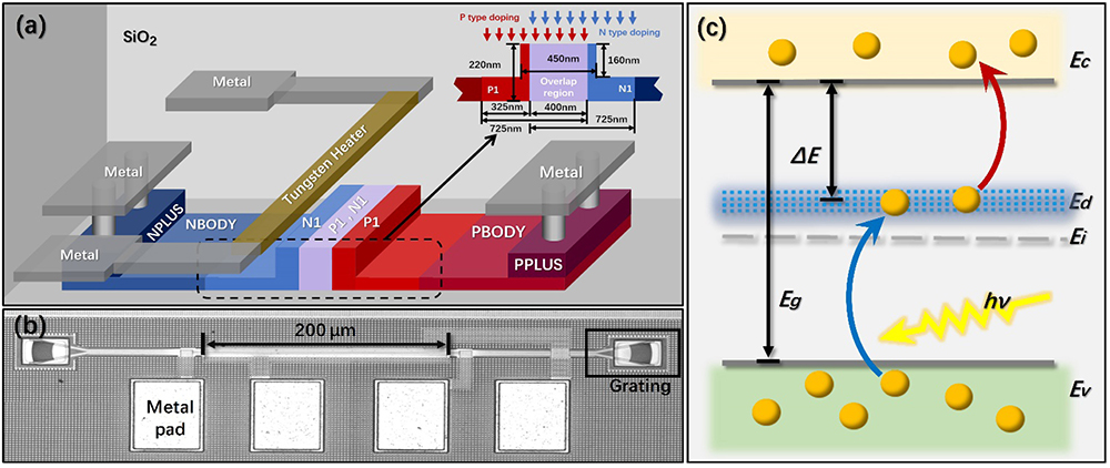
    Fig. 1. (a) Three-dimensional schematic diagram, cross section, and doping pattern of the in-line optical power monitor based on the BDA effect. (b) Top-view microscope image of the all-silicon in-line optical power monitor based on the BDA effect. (c) Schematic diagram of the BDA process inside the silicon waveguide.
    (a) Experimental setup to test the insertion loss and the responsivity of the DUT. (b) Transmission spectra of the DUT with 2-mm-long absorption region and the passive straight waveguide. The output power of the laser is 0 dBm. (c) Waveguide propagation losses of the DUT versus reverse bias voltages. (d) and (e) Photocurrents versus on-chip incident optical powers of the DUT with 0.2-mm-long absorption region at room temperature and 550 mW heating power.
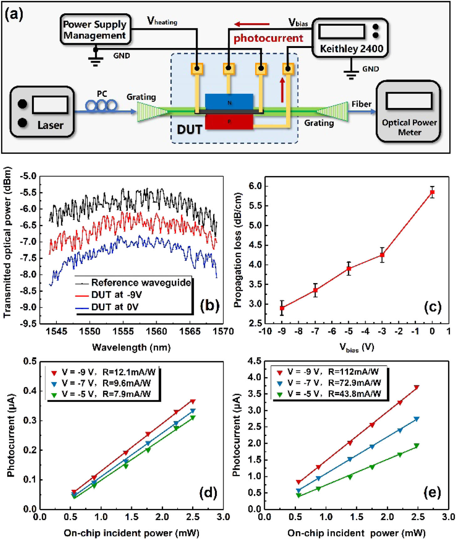
    Fig. 2. (a) Experimental setup to test the insertion loss and the responsivity of the DUT. (b) Transmission spectra of the DUT with 2-mm-long absorption region and the passive straight waveguide. The output power of the laser is 0 dBm. (c) Waveguide propagation losses of the DUT versus reverse bias voltages. (d) and (e) Photocurrents versus on-chip incident optical powers of the DUT with 0.2-mm-long absorption region at room temperature and 550 mW heating power.
    (a) Responsivity and (b) dark current as a function of the heating power at two different reverse biases. Discrete points denote measurement results, while fitted curves are displayed in solid lines. Fitted parameter values are given inside the legend.
    Fig. 3. (a) Responsivity and (b) dark current as a function of the heating power at two different reverse biases. Discrete points denote measurement results, while fitted curves are displayed in solid lines. Fitted parameter values are given inside the legend.
    NEPs of the DUT versus heating powers at two different bias voltages. The inset shows the theoretical minimum detectable incident powers of DUT as a function of the heating power.
    Fig. 4. NEPs of the DUT versus heating powers at two different bias voltages. The inset shows the theoretical minimum detectable incident powers of DUT as a function of the heating power.
    (a) Schematic diagram of the optical power monitoring system operating in the sampling mode. (b) Output voltage waveforms of the TIA in response to 180-μs-wide heating pulses with different peak power levels. Dark current has been calibrated.
    Fig. 5. (a) Schematic diagram of the optical power monitoring system operating in the sampling mode. (b) Output voltage waveforms of the TIA in response to 180-μs-wide heating pulses with different peak power levels. Dark current has been calibrated.
    Voltage outputs of the optical power monitoring system versus on-chip incident optical powers under a heating power of (a) 300 mW and (b) 550 mW. Linear fittings of experimental data are implemented to obtain power-to-voltage responsivities of the system. The two insets present noise outputs of the system in the dark condition. The two blue dotted lines give RMS noise voltage levels of the system.
    Fig. 6. Voltage outputs of the optical power monitoring system versus on-chip incident optical powers under a heating power of (a) 300 mW and (b) 550 mW. Linear fittings of experimental data are implemented to obtain power-to-voltage responsivities of the system. The two insets present noise outputs of the system in the dark condition. The two blue dotted lines give RMS noise voltage levels of the system.
    Ref.TypeOriginal ResponsivityEnhancement MethodEnhanced ResponsivityLossLength/Radius
    [32]pinAvalanche10 A/W (20  V)20 dB/cmL=2  mm
    [27]pin0.3 mA/W (0 V)Avalanche+Resonant39 mA/W (20V)10.8 dB/cmR=20  μm
    [33]pinAvalanche+Resonant0.16 A/W (20  V)26.9 dB/cmR=20  μm
    [35]pinResonant23 mA/W (5  V)R=20  μm
    [26]pin3.2 mA/W (5  V)Avalanche4.7 A/W (40  V)79 dB/cmL=600  μm
    [28]pn1.6 mA/W (5  V)Avalanche+Resonant72.8 mA/W (8  V)153 dB/cmL=102  μm
    [24]pin8 mA/W7 dB/cmL=5  mm
    [36]pnAvalanche7 mA/W (3  V)10 dB/cmL=1.4  mm
    [25]pin5 mA/W (5  V)Avalanche0.3 A/W (30  V)3 dB/cmL=1  mm
    [29]pn5.1 mA/W (5  V)Avalanche+Resonant48 mA/W (8  V)16.7 dB/cmL=67  μm
    [17]pn0.17 mA/W (4  V)35 dB/cmL=66  μm
    [30]pn4.7 mA/W (3  V)Avalanche0.54 A/W (9  V)30 dB/cmL=1  mm
    Our workpin12.1 mA/W (9  V)Heating0.112 A/W (9  V)2.9 dB/cmL=200  μm
    Table 1. Comparison of the DC Responsivity Between Our Device and Previously Reported NIR BDA-Based Si PDs
    Qikai Huang, Hui Yu, Qiang Zhang, Yan Li, Weiwei Chen, Yuehai Wang, Jianyi Yang. Thermally enhanced responsivity in an all-silicon optical power monitor based on defect-mediated absorption[J]. Photonics Research, 2021, 9(11): 2205
    Download Citation