
Qikai Huang, Hui Yu, Qiang Zhang, Yan Li, Weiwei Chen, Yuehai Wang, Jianyi Yang. Thermally enhanced responsivity in an all-silicon optical power monitor based on defect-mediated absorption[J]. Photonics Research, 2021, 9(11): 2205
- Photonics Research
- Vol. 9, Issue 11, 2205 (2021)
Abstract
1. INTRODUCTION
Silicon photonics technology now plays important roles in fields of optical communication [1,2], optical quantum computing [3,4], biochemistry sensing [5,6], light detection and ranging (LiDAR) [7,8], optical neuromorphic networks, and deep learning [9,10], thanks to its advantages in compatibility with CMOS fabrication technology and excellent light-guiding characteristics at telecom/datacom wavelengths. Significant advances have been made in developing a variety of large-scale silicon photonic integrated circuits (PICs) with very high integration levels [11,12]. It is well known that performances and optimal operating points of most silicon photonics devices are quite sensitive to fabrication errors and ambient temperature fluctuations. Therefore, as the complexity of silicon PICs increases, it becomes essential to acquire optical power levels at critical positions of the circuits so as to build feedback control loops. This task is implemented by the optical power monitor, which is demanded to probe the optical power with a minimal intervention to the light propagation inside the circuit [13,14]. A straightforward solution is to tap a small portion of the propagated light to a terminal Ge/Si waveguide photodetector through a directional coupler (DC) [15,16]. However, this scheme suffers from limited scalability. Additionally, coupling efficiencies of silicon DCs are susceptible to the wavelength and the fabrication-imperfection induced variation of coupling gap. As a result, a preferable alternative is an in-line all-silicon optical power monitor that can be directly embedded inside the optical route [17,18]. An ideal in-line optical power monitor should possess a relatively weak absorption coefficient and a high responsivity. With a proper absorption length, only a small fraction of the incident light is converted to photocarriers while most of the light can pass through.
Since the intrinsic absorption in silicon is very weak at wavelengths longer than 1.1 μm, all-silicon optical power monitors resort to two-photon absorption (TPA) [19,20], internal photoemission effect (IPE) [21,22], or bulk deep-level defect-mediated absorption (BDA) [23,24]. Among them, the BDA effect is the most widely utilized. This effect relies on ion implantation and rapid annealing steps to introduce lattice defects inside the silicon. These lattice defects act as transition states through which valence band electrons can jump to the conduction band by absorbing sub-bandgap photons. Compared with the intrinsic absorption, a disadvantage of the BDA effect is its low quantum efficiency. Without utilizing enhancement mechanisms such as the optical resonance effect or the avalanche multiplication effect, the typical responsivities of practical BDA-based photodiodes are usually less than 10 mA/W [24–30]. Consequent weak photocurrents result in additional difficulty and cost in the subsequent circuit design. For example, if the optical power transmitted inside an optical link is and 2% of it is absorbed by a BDA monitor with a responsivity of 10 mA/W, the resultant photocurrent is . In order to produce a feedback signal with sufficiently high voltage level on the order of a few hundred millivolts, a magnification ratio higher than is necessary, which imposes a stringent requirement on the amplifying circuit design especially when a wide bandwidth is also required.
There are plenty of efforts to increase responsivities of BDA photodiodes. A straightforward way is applying large reverse bias voltages so that diodes operate in the avalanche regime. Reported responsivities can be boosted to several tens of mA/W or even higher [25,26]. However, reverse bias voltages to obtain sufficient avalanche gains are usually much higher than 20 V provided that PIN junctions are utilized to collect photocarriers [25–27,31–33]. These bias conditions are ill-suited for many application scenarios. Although avalanche voltages less than 10 V can be realized by utilizing PN junctions with doping concentrations on the order of [28–30], this doping pattern inevitably increases the optical loss aroused by the free carrier absorption. Alternatively, the responsivity of BDA effect can be enhanced by resonant cavities at the expenses of narrow optical bandwidth and low scalability [33–35]. Besides, the avalanche multiplication effect and the resonance enhancement effect are combined routinely in many reports [28,29,36]. Despite these achievements, it is still quite a challenge to realize a BDA effect-based optical power monitor with all the necessary merits demanded by practical applications, i.e., high responsivity, low bias voltage, low insertion loss, and large bandwidth. As a result, almost all advanced silicon PICs ultimately rely on Si/Ge waveguide photodetectors (PDs) with DCs to monitor their operation conditions.
Sign up for Photonics Research TOC. Get the latest issue of Photonics Research delivered right to you!Sign up now
In this work, we first propose and demonstrate a thermal enhancement technique to boost the responsivity of BDA effect. By pulse-heating the light absorption region, we improve the responsivity of a 200-μm-long all-silicon optical power monitor from 12.1 mA/W to 112 mA/W. Average power and instantaneous peak power of the heater that operates in the pulsed mode are 1 mW and 550 mW, respectively. The insertion loss of the device is as low as 0.06 dB. Compared with avalanche multiplication and resonance enhancement effects, this technique possesses advantages of high responsivity, low bias voltage, low insertion loss, high scalability, and wide optical bandwidth and, thus, is qualified to build feedback control systems of practical silicon PICs. This work is organized as follows. At first, we introduce design, fabrication, and operation principle of our device in Sections 2 and 3. After that, control circuit design and measurement results are presented in Section 4. Finally, a conclusion is reached in Section 5 by systematically comparing our device with previous works.
2. DEVICE DESIGN AND FABRICATION
The BDA effect based all-silicon optical power monitor is an SOI rib waveguide with an embedded PN junction as shown in Fig. 1(a). The doping compensation technique we developed in Ref. [37] is used to introduce lattice defects necessary for the sub-bandgap optical absorption. This technique directly takes advantage of the existing P/N ion implantation steps that are used to build carrier-depletion-based silicon modulators. By overlapping P/N ion implantation windows, a dopant compensation region is formed in the waveguide center. The repeated ion bombardment steps create a quasi-intrinsic region due to the compensation between two opposite dopants and, thus, suppress the unnecessary free carrier absorption. On the other hand, the lattice defect density is approximately doubled to cause a larger photocurrent. After ion implantation steps, a rapid thermal annealing (RTA) above 1000°C repairs most lattice damages. The sub-bandgap absorption is enabled by the remaining lattice defects. This scheme is implemented by the unmodified standard processing flow of active silicon photonic devices. But its responsivity is comparable or even better than reported BDA devices that utilize specialized ion implantation and annealing steps to introduce lattice defects. The feature of our device is that its responsivity is boosted by a tungsten heater. The theory behind this thermal enhancement effect will be explained in Section 3.
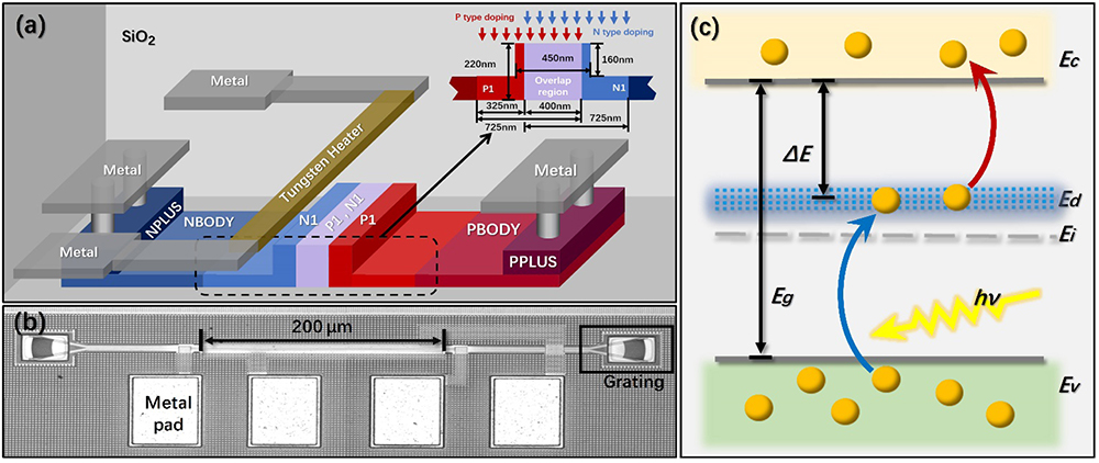
Figure 1.(a) Three-dimensional schematic diagram, cross section, and doping pattern of the in-line optical power monitor based on the BDA effect. (b) Top-view microscope image of the all-silicon in-line optical power monitor based on the BDA effect. (c) Schematic diagram of the BDA process inside the silicon waveguide.
The device is fabricated by the silicon photonics multi-project wafer (MPW) service of IMEC (ISIPP50G) on an SOI wafer with a 220-nm-thick Si layer and a 2-μm-thick buried oxide (BOX) layer. The width of the rib waveguide shown in Fig. 1(a) is 450 nm. Two 1.3-μm-wide trenches are etched by 160 nm beside the waveguide so as to provide the optical confinement. Both P1-type and N1-type ion implantation windows are 725 nm wide. The two windows overlap by 400 nm in the waveguide center to form a doping compensation region. The final widths of lightly doped P1 and N1 regions, thus, are 325 nm as shown in the inset of Fig. 1(a). PBODY/NBODY regions are 300 nm away from waveguide sidewalls. They are moderately doped to reduce series resistances between the junction and the contacts. PPLUS/NPLUS regions are heavily doped to form ohmic contacts. Corresponding ion implantation conditions are determined by optimizing the performance of the carrier-depletion-based modulator. Measured avalanche breakdown voltage of this diode is . The length of optical absorption region is 200 μm. The resistance of tungsten heater above the waveguide is 160 Ω. In order to facilitate the optical propagation loss measurement, another device with a 2-mm-long optical absorption region is also designed. Fiber grating couplers are used to interface the device with input/output fibers. A microscope image of our device is displayed in Fig. 1(b).
3. THERMAL ENHANCEMENT MECHANISM
We shortly review the BDA effect before explaining how a heater helps to improve the responsivity. As depicted in Fig. 1(c), the BDA consists of two steps. At first, a sub-bandgap photon excites an electron from the valence band to the defect energy levels below the conduction band. After that, a part of excited electrons can jump to the conduction band through the thermal excitation and, thus, become photocarriers. The rest electrons stay in defect energy levels or fall to the valence band until finally reaching a dynamic equilibrium. The optical excitation rate of the first step is mainly determined by the incident photon energy, the absorption area, and the concentration of defects [38]. According to the Shockley–Read–Hall (SRH) theory and its extension to optical generation by sub-bandgap photons [39,40], the thermal excitation rate can be calculated as
By examining the temperature dependence of every term in Eq. (1), we can quantitatively estimate the thermal enhancement factor of the responsivity. At first, the correlation between effective mass and temperature is very weak. Second, the dependence of the intrinsic carrier concentration on the temperature can be written as , where is the bandgap of silicon [42]. Third, the thermal velocity of electrons in silicon is proportional to [43]. Finally, the thermal excitation rate in thermal equilibrium can be approximated as . Here denotes the bottom of conduction band. While emitting electrons toward the conduction band, defect energy levels also capture electrons from the conduction band. The corresponding capture rate varies with the temperature in a similar manner to [40]. To simplify the discussion, we assume that the responsivity is proportional to the net generation rate of photocarriers, i.e., the difference between the excitation rate and the capture rate. Moreover, considering the temperature dependence of , the relationship between the responsivity and the temperature can be simplified as
The exact value of the positive constant can be obtained by fitting the experimental data.
Raising the operation temperature also enhances the dark current noise of the PD and eventually deteriorates the detectivity. This adverse effect should also be investigated to justify the feasibility of this technique. It is known that the dark current noise of a PD is mainly composed of the shot noise [44] and the Johnson noise [45]. The root-mean-square (RMS) value of the Johnson noise is proportional to the temperature, while that of the shot noise is proportional to the DC component of the dark current, i.e., the diffusion current. Therefore, the shot noise presents a similar temperature dependence to the DC diffusion current. According to the Shockley law, the DC diffusion current of a reversely biased PN junction in the non-avalanche region is written as [46]
According to the analysis in Ref. [49], a positive parameter is introduced here to reflect the influence of the reverse bias voltage. Its value would decrease as the reverse bias voltage grows. A typical variation range is between 0 and 1. The DC diffusion current and the corresponding shot noise usually grow with the temperature at a much higher rate than the responsivity. Therefore, there is a trade-off between the responsivity enhancement and the detectivity degradation when we heat the device.
The detectivity of a PD is characterized by the noise-equivalent-power (NEP) [50]. It is defined as the net absorbed power level at which the generated photocurrent is equal to the square root of the noise power spectral density measured within a specified bandwidth, i.e., . Here is the responsivity of the PD. is the measured noise bandwidth. The noise power spectral density is calculated as . Here, is the Fourier transform of the dark current fluctuation acquired within a time period of .
Unlike the terminal PD, an in-line optical power monitor absorbs only a small fraction of the incident optical power, so its minimum detectable incident power (MDP) is calculated as . Here and denote the propagation loss of the in-line optical power monitor in unit of dB/cm and the absorption region length, respectively. If the absorption region is long enough so that the incident power is absorbed completely, i.e., , MDP is numerically equal to the NEP.
4. EXPERIMENTS AND RESULTS
The setup of responsivity measurement is shown in Fig. 2(a). The output light of a C-band tunable laser (Santec-TSL-510) passes through a polarization controller (PC), and then is coupled to the device under test (DUT) by a fiber grating coupler. Only a small portion of the incident light is absorbed by the DUT, while the rest is fed into an optical powermeter (OPM) by another fiber grating coupler. A sourcemeter (Keithley 2400) provides the reverse bias for the DUT and reads the photocurrent. Another current source provides the heating current for the tungsten heater.
![]()
Figure 2.(a) Experimental setup to test the insertion loss and the responsivity of the DUT. (b) Transmission spectra of the DUT with 2-mm-long absorption region and the passive straight waveguide. The output power of the laser is 0 dBm. (c) Waveguide propagation losses of the DUT versus reverse bias voltages. (d) and (e) Photocurrents versus on-chip incident optical powers of the DUT with 0.2-mm-long absorption region at room temperature and 550 mW heating power.
By sweeping the wavelength of tunable laser and the reverse bias voltage, we measure transmission spectra of the long device with the 2-mm-long absorption region. Results are displayed in Fig. 2(b) as well as the transmission spectrum of a reference straight waveguide on the same chip. By comparing power levels of different spectra in Fig. 2(b), we extract the dependence of the waveguide propagation loss on the voltage in Fig. 2(c). As the reverse bias increases from 0 V to , the propagation loss falls from to due to the depletion of free carriers. In contrast, the undoped strip waveguide on the same chip exhibits a propagation loss of 1.4 dB/cm, while the modulator waveguide with no overlapping between P1 and N1 implantation windows exhibits a propagation loss of 13.8 dB/cm at 0 V. Therefore, the doping compensation technique substantially suppresses the free carrier absorption loss and is beneficial for reducing the intervention to the function of the PIC. We also note that the variation of propagation loss is inappreciable when we heat the waveguide.
In the following context, our measurement is focused on the 0.2-mm-long device, which is adjacent to the 2-mm-long device. Owing to the measurement error as shown in Fig. 2(b), the on-chip insertion loss of the 0.2-mm-long device is too small to be measured directly. However, according to the measured waveguide propagation loss per unit length of the 2-mm-long device in Fig. 2(c), the insertion loss of the 0.2-mm-long device at is calculated as . Its photocurrents at room temperature versus on-chip incident optical powers are plotted in Fig. 2(d) under different bias conditions. Corresponding responsivities are 7.9/9.6/12.1 mA/W at . Here the responsivity is defined as the ratio of the photocurrent to the net absorbed power. The net absorbed power is calculated according to the measured waveguide propagation loss in Fig. 2(c), the absorption region length, and the on-chip incident optical power. In Fig. 2(e), responsivity measurements are performed under a heating power of 550 mW. Compared with Fig. 2(d), responsivities in Fig. 2(e) are boosted significantly to 43.8/72.9/112 mA/W at . Since the reverse bias voltages in these measurements are much less than the measured avalanche voltage of , there is no avalanche gain. The responsivity enhancement with the reverse bias in Figs. 2(d) and 2(e), thus, can be attributed to the improved collection efficiency of photo-generated carriers.
Measured responsivities and dark currents versus heating powers are plotted as discrete points in Figs. 3(a) and 3(b), respectively. We then use expressions in Eqs. (2) and (4) to fit measured temperature dependences of the responsivity and the dark current, respectively. Fitted curves are plotted in Fig. 3 as solid lines, while values of and that provide the optimal fitting results are labeled in the figure legends. Here we have assumed that the temperature increment is proportional to the heating power, i.e., . The proportionality factor reflects the heating efficiency. Its value is 0.64 K/mW according to our numerical simulation results. The coincidence between fitting curves and measurement data justifies our theoretical analysis of the thermal enhancement mechanism in Section 3.
![]()
Figure 3.(a) Responsivity and (b) dark current as a function of the heating power at two different reverse biases. Discrete points denote measurement results, while fitted curves are displayed in solid lines. Fitted parameter values are given inside the legend.
Noise power spectral densities of our device under different heating powers are characterized with the method described in Section 3. The dark current fluctuation is acquired by a current meter operating at a sampling frequency of 5 kHz. The total number of sampling points is 5000. The bandwidth, thus, is 2.5 kHz with a resolution bandwidth of 1 Hz. The NEP results are plotted in Fig. 4 as a function of the heating power. Furthermore, NEPs are converted to theoretical MDPs of the DUT in the inset of Fig. 4. As already discussed in Section 3, heating the device enhances both the noise power spectral density and the responsivity . Before the heating power rises to 300 mW, the two NEP curves are almost flat. We speculate the reason is that the noise of the DUT in this region is quite low and, thus, is overwhelmed by the background noise of the measurement setup shown in Fig. 2(a). The NEP decreases slightly mainly due to the enhanced responsivity. Once the heating power rises above 300 mW, the noise of the DUT becomes the dominant factor and grows rapidly with the temperature. Since rises much faster than , the final NEP deteriorates rapidly. At a heating power of 300 mW, the device provides NEPs of and at and , respectively. When the heating power rises to 550 mW, the NEPs at and degrade to and , respectively. However, even under this worst condition, corresponding MDPs are far below optical power levels in most practical optical communication links [51]. We also note that the NEP is improved by increasing the reverse bias voltage. This can be attributed to the enhanced responsivity and the insensitivity of the noise power spectral density against the reverse bias in the non-avalanche region.
![]()
Figure 4.NEPs of the DUT versus heating powers at two different bias voltages. The inset shows the theoretical minimum detectable incident powers of DUT as a function of the heating power.
We find that calculated shot noises on basis of measured dark currents in Fig. 3(b) are far lower than measured noise levels. Therefore, we speculate that the Johnson noise and the background noises of measurement instruments are the main noise source.
We are also aware that the power consumption of a few hundred milliwatts would impede the practical application of this technique. However, it is not really necessary to maintain the device at such a high temperature and probe the optical power continuously. Instead, the device can operate in the sampling mode. In this mode, the device is heated by a periodic rectangular pulse signal whose pulse width is slightly longer than the time constant of the thermo-optical effect. Once the temperature reaches the steady state near the end of each pulse, the optical power level is acquired swiftly with the enhanced responsivity. The average heating power, thus, is proportional to the duty cycle of the periodic pulse signal. The sampling rate can be set flexibly according to the specific requirement. The setup enabling this operation mode is presented in Fig. 5(a). A micro-programmed control unit (MCU) provides a periodical rectangular pulse signal to control an analog switch. The power supply management module provides both the heating current and the reverse bias voltage for the DUT and records corresponding output powers in the meantime. When the analog switch is in the “on” state, a current drives the tungsten heater to enhance the responsivity. The generated photocurrent signal then is converted to a voltage signal by a transimpedance amplifier (TIA). The buffer circuit plays the roles of impedance transformation and isolation. After the buffer circuit, the analog voltage signal is sampled and converted to the digital signal by an analog-to-digital converter (ADC). Finally, the digital voltage signal is sent to the MCU as a feedback control signal for the subsequent data processing.
![]()
Figure 5.(a) Schematic diagram of the optical power monitoring system operating in the sampling mode. (b) Output voltage waveforms of the TIA in response to 180-μs-wide heating pulses with different peak power levels. Dark current has been calibrated.
In Fig. 5(b), we present output voltage waveforms of the TIA as well as the 180-μs-wide rectangular control pulse (gray) produced by the MCU. The on-chip incident power and the reverse bias in the measurement are and , respectively. The duration of the rectangular pulse is determined as the sum of the rise time of thermo-optical effect and the conversion time of the ADC. It is apparent that after heating the DUT by 160 μs, output voltages enter the steady state. Voltage ripples in the steady state can be attributed to circuit noises of the TIA and the power supply. The ADC in this work offers a throughput rate of 1 MS/s, so a full ADC conversion cycle takes around 1 μs. In order to improve the measurement accuracy, we repeat the ADC sampling by 20 times and then calculate the average of 20 sampling results. Therefore, the overall time necessary to perform a reliable optical power measurement is . Given that the peak power of the rectangular pulse driving the heater is (in mW) and the optical power measurement is repeated by times a second, the average power consumption of the device is (in μW).
Measured average voltages versus on-chip incident powers at 300 mW and 550 mW are plotted in Figs. 6(a) and 6(b), respectively. The slopes of linearly fitted lines in Fig. 6 represent the optical-power-to-voltage responsivities of the whole optical power monitoring module. In order to characterize the detectivity of the whole module, we test noise outputs of the ADC by shutting down the laser in two insets of Fig. 6. The two blue dotted lines in Fig. 6 give RMS noise voltages () of the system. The results indicate that the noise amplitude at 300 mW is very close to that at 550 mW. In contrast, the measured NEP of the stand-along DUT in Fig. 4 rises by as the heating power increases from 300 mW to 550 mW. We speculate the reason for this discrepancy is that the noise of the overall system is dominated by circuit elements rather than the DUT. In this case, a higher responsivity is obtained with a little penalty on the noise output when we heat the device. At an instantaneous heating power of 550 mW, the minimum detectable optical power of the system is under a reverse bias of . In addition, the value of is chosen to be in our experiment, so the resultant average power consumption is .
![]()
Figure 6.Voltage outputs of the optical power monitoring system versus on-chip incident optical powers under a heating power of (a) 300 mW and (b) 550 mW. Linear fittings of experimental data are implemented to obtain power-to-voltage responsivities of the system. The two insets present noise outputs of the system in the dark condition. The two blue dotted lines give RMS noise voltage levels of the system.
5. CONCLUSION
In conclusion, we first demonstrate a thermal enhancement technique to boost the responsivity of BDA effect in the silicon waveguide. The all-silicon in-line optical power monitor utilizing this technique provides a low insertion loss of 0.06 dB and a high responsivity of 112 mA/W at bias. The MDP of the optical power monitoring module composed of this device and related circuits is less than . The extra heating power is less than 1 mW.
We summarized the performance of previously reported all-silicon photodiodes that utilize the BDA effect in Table 1. It can be seen that avalanche multiplication and resonance enhancement effects are extensively utilized to improve the weak photoelectronic conversion efficiency of the BDA effect. Despite a lot of efforts, they are difficult to be employed by practical silicon PICs due to the reason that none of these devices are able to simultaneously provide a relatively low loss and a low operating voltage below 10 V, as well as a high responsivity beyond 100 mA/W. In contrast, our device possesses all these advantages with the expense of a very low average heating power. The low insertion loss of our device is very close to that of the contactless integrated photonic probe (CLIPP) () reported in Ref. [52]. Another advantage featured by our device is that it is manufactured by the open-access silicon photonics MPW service without using any customized processing steps. Comparison of the DC Responsivity Between Our Device and Previously Reported NIR BDA-Based Si PDsRef. Type Original Responsivity Enhancement Method Enhanced Responsivity Loss Length/Radius [ pin — Avalanche 10 A/W ( 20 dB/cm [ pin 0.3 mA/W (0 V) 39 mA/W 10.8 dB/cm [ pin — 0.16 A/W ( 26.9 dB/cm [ pin — Resonant 23 mA/W ( — [ pin 3.2 mA/W ( Avalanche 4.7 A/W ( 79 dB/cm [ pn 1.6 mA/W ( 72.8 mA/W ( 153 dB/cm [ pin 8 mA/W — — 7 dB/cm [ pn — Avalanche 7 mA/W ( 10 dB/cm [ pin 5 mA/W ( Avalanche 0.3 A/W ( 3 dB/cm [ pn 5.1 mA/W ( 48 mA/W ( 16.7 dB/cm [ pn 0.17 mA/W ( — — 35 dB/cm [ pn 4.7 mA/W ( Avalanche 0.54 A/W ( 30 dB/cm Our work pin 12.1 mA/W ( Heating 0.112 A/W ( 2.9 dB/cm
The device in this work represents a proof-of-principle demonstration of the thermal enhancement technique. Future performance improvement can be focused to reduce the power consumption of the heater. This can be implemented from two aspects. At first, the theoretical model in Section 2 indicates that, if the defect energy level goes down by 0.1 eV, the temperature rise to induce the same enhancement factor of the responsivity can be reduced by about 5 times. It is known that the position of the defect energy level depends on specific ion implantation conditions such as dopant species, implantation dose, and energy [41,53]. As a result, it is suggested to tune the defect energy level by customizing ion implantation conditions. Second, the heater in this work has not used any advanced designs and, thus, presents a relatively poor heating efficiency. Actually, various heater structures such as free-standing waveguides with undercut and thermal isolation trenches have been widely reported [54,55]. They successfully improve the heating efficiencies of silicon waveguides by over 10 times. With these two measures, we believe that the power consumption of our device can be reduced by more than 50 times so as to meet stringent power requirements of practical optical communication systems.
References
[1] Q. Cheng, M. Bahadori, M. Glick, S. Rumley, K. Bergman. Recent advances in optical technologies for data centers: a review. Optica, 5, 1354-1370(2018).
[2] R. Kakarla, J. Schroder, P. A. Andrekson. One photon-per-bit receiver using near-noiseless phase-sensitive amplification. Light Sci. Appl., 9, 153(2020).
[3] J. Carolan, C. Harrold, C. Sparrow, E. Martín-López, N. J. Russell, J. W. Silverstone, P. J. Shadbolt, N. Matsuda, M. Oguma, M. Itoh, G. D. Marshall, M. G. Thompson, J. C. F. Matthews, T. Hashimoto, J. L. O’Brien, A. Laing. Universal linear optics. Science, 349, 711-716(2015).
[4] N. C. Harris, G. R. Steinbrecher, M. Prabhu, Y. Lahini, J. Mower, D. Bunandar, C. Chen, F. N. C. Wong, T. Baehr-Jones, M. Hochberg, S. Lloyd, D. Englund. Quantum transport simulations in a programmable nanophotonic processor. Nat. Photonics, 11, 447-452(2017).
[5] K. D. Vos, I. Bartolozzi, E. Schacht, P. Bienstman, R. Baets. Silicon-on-insulator microring resonator for sensitive and label-free biosensing. Opt. Express, 15, 7610-7615(2007).
[6] J. T. Robinson, C. Long, M. Lipson. On-chip gas detection in silicon optical microcavities. Opt. Express, 16, 4296-4301(2008).
[7] R. Fatemi, A. Khachaturian, A. Hajimiri. A nonuniform sparse 2-D large-FOV optical phased array with a low-power PWM drive. IEEE J. Solid-State Circuits, 54, 1200-1215(2019).
[8] C. V. Poulton, M. J. Byrd, P. Russo, E. Timurdogan, M. Khandaker, D. Vermeulen, M. R. Watts. Long-range LiDAR and free-space data communication with high-performance optical phased arrays. IEEE J. Sel. Top. Quantum Electron., 25, 17700108(2019).
[9] Y. Shen, N. C. Harris, S. Skirlo, M. Prabhu, T. Baehr-Jones, M. Hochberg, X. Sun, S. Zhao, H. Larochelle, D. Englund, M. Soljačić. Deep learning with coherent nanophotonic circuits. Nat. Photonics, 11, 441-446(2017).
[10] X. Lin, Y. Rivenson, N. T. Yardimci, M. Veli, Y. Luo, M. Jarrahi, A. Ozcan. All-optical machine learning using diffractive deep neural networks. Science, 361, 1004-1008(2018).
[11] W. Bogaerts, D. Perez, J. Capmany, D. A. B. Miller, J. Poon, D. Englund, F. Morichetti, A. Melloni. Programmable photonic circuits. Nature, 586, 207-216(2020).
[12] D. Marpaung, J. Yao, J. Capmany. Integrated microwave photonics. Nat. Photonics, 13, 80-90(2019).
[13] T. Komljenovic, P. Pintus. On-chip calibration and control of optical phased arrays. Opt. Express, 26, 3199-3210(2018).
[14] L. Qiao, W. Tang, T. Chu. 32 × 32 silicon electro-optic switch with built-in monitors and balanced-status units. Sci. Rep., 7, 42306(2017).
[15] P. Dong, R. Gatdula, K. Kim, J. H. Sinsky, A. Melikyan, Y.-K. Chen, G. de Valicourt, J. Lee. Simultaneous wavelength locking of microring modulator array with a single monitoring signal. Opt. Express, 25, 16040-16046(2017).
[16] Q. Zhu, C. Qiu, Y. He, Y. Zhang, Y. Su. Self-homodyne wavelength locking of a silicon microring resonator. Opt. Express, 27, 36625-36636(2019).
[17] Z. Wang, D. Paez, A. I. A. El-Rahman, P. Wang, L. Dow, J. C. Cartledge, A. P. Knights. Resonance control of a silicon micro-ring resonator modulator under high-speed operation using the intrinsic defect-mediated photocurrent. Opt. Express, 25, 24827-24836(2017).
[18] A. Ribeiro, A. Ruocco, L. Vanacker, W. Bogaerts. Demonstration of a 4 × 4-port universal linear circuit. Optica, 3, 1348-1357(2016).
[19] R. Hayakawa, N. Ishikura, H. C. Nguyen, T. Baba. Two-photon-absorption photodiodes in Si photonic-crystal slow-light waveguides. Appl. Phys. Lett., 102, 031114(2013).
[20] H. Zhu, L. Zhou, R. Yang, X. Li, J. Chen. Enhanced near-infrared photodetection with avalanche gain in silicon microdisk resonators integrated with p-n diodes. Opt. Lett., 39, 4525-4528(2014).
[21] S. Zhu, H. S. Chu, G. Q. Lo, P. Bai, D. L. Kwong. Waveguide-integrated near-infrared detector with self-assembled metal silicide nanoparticles embedded in a silicon p-n junction. Appl. Phys. Lett., 100, 061109(2012).
[22] I. Goykhman, U. Sassi, B. Desiatov, N. Mazurski, S. Milana, D. de Fazio, A. Eiden, J. Khurgin, J. Shappir, U. Levy, A. C. Ferrari. On-chip integrated, silicon–graphene plasmonic Schottky photodetector with high responsivity and avalanche photogain. Nano Lett., 16, 3005-3013(2016).
[23] H. Yu, D. Korn, M. Pantouvaki, J. Van Campenhout, K. Komorowska, P. Verheyen, G. Lepage, P. Absil, D. Hillerkuss, L. Alloatti, J. Leuthold, R. Baets, W. Bogaerts. Using carrier-depletion silicon modulators for optical power monitoring. Opt. Lett., 37, 4681-4683(2012).
[24] D. J. Thomson, L. Shen, J. J. Ackert, E. Huante-Ceron, A. P. Knights, M. Nedeljkovic, A. C. Peacock, G. Z. Mashanovich. Optical detection and modulation at 2 μm–2.5 μm in silicon. Opt. Express, 22, 10825-10830(2014).
[25] J. J. Ackert, D. J. Thomson, L. Shen, A. C. Peacock, P. E. Jessop, G. T. Reed, G. Z. Mashanovich, A. P. Knights. High-speed detection at two micrometres with monolithic silicon photodiodes. Nat. Photonics, 9, 393-396(2015).
[26] J. J. Ackert, A. S. Karar, D. J. Paez, P. E. Jessop, J. C. Cartledge, A. P. Knights. 10 Gbps silicon waveguide-integrated infrared avalanche photodiode. Opt. Express, 21, 19530-19537(2013).
[27] D. F. Logan, P. Velha, M. Sorel, R. M. De La Rue, A. P. Knights, P. E. Jessop. Defect-enhanced silicon-on-insulator waveguide resonant photodetector with high sensitivity at 1.55 μm. IEEE Photon. Technol. Lett., 22, 1530-1532(2010).
[28] Y. Li, S. Feng, Y. Zhang, A. W. Poon. Sub-bandgap linear-absorption-based photodetectors in avalanche mode in PN-diode-integrated silicon microring resonators. Opt. Lett., 38, 5200-5203(2013).
[29] X. Li, Z. Li, X. Xiao, H. Xu, J. Yu, Y. Yu. 40 Gb/s all-silicon photodetector based on microring resonators. IEEE Photon. Technol. Lett., 27, 729-732(2015).
[30] H. Zhu, K. Goi, K. Ogawa. All-silicon waveguide photodetection for low-bias power monitoring and 20-km 28-Gb/s NRZ-OOK signal transmission. IEEE J. Sel. Top. Quantum Electron., 24, 4400207(2018).
[31] M. W. Geis, S. J. Spector, M. E. Grein, R. T. Schulein, J. U. Yoon, D. M. Lennon, C. M. Wynn, S. T. Palmacci, F. Gan, F. X. Kaertner, T. M. Lyszczarz. All silicon infrared photodiodes: photo response and effects of processing temperature. Opt. Express, 15, 16886-16895(2007).
[32] M. W. Geis, S. J. Spector, M. E. Grein, J. U. Yoon, D. M. Lennon, T. M. Lyszczarz. Silicon waveguide infrared photodiodes with >35 GHz bandwidth and phototransistors with 50 AW-1 response. Opt. Express, 17, 5193-5204(2009).
[33] D. F. Logan, K. J. Murray, J. J. Ackert, P. Velha, M. Sorel, R. M. De La Rue, P. E. Jessop, A. P. Knights. Analysis of resonance enhancement in defect-mediated silicon micro-ring photodiodes operating at 1550 nm. J. Opt., 13, 125503(2011).
[34] D. F. Logan, P. Velha, M. Sorel, R. M. De La Rue, P. E. Jessop, A. P. Knights. Monitoring and tuning micro-ring properties using defect-enhanced silicon photodiodes at 1550 nm. IEEE Photon. Technol. Lett., 24, 261-263(2012).
[35] J. J. Ackert. Silicon-on-insulator microring resonator defect-based photodetector with 3.5-GHz bandwidth. J. Nanophoton., 5, 059507(2011).
[36] B. Desiatov, I. Goykhman, J. Shappir, U. Levy. Defect-assisted sub-bandgap avalanche photodetection in interleaved carrier-depletion silicon waveguide for telecom band. Appl. Phys. Lett., 104, 091105(2014).
[37] Q. Zhang, H. Yu, T. Qi, Z. Fu, X. Jiang, J. Yang. Enhancing bulk defect-mediated absorption in silicon waveguides by doping compensation technique. Sci. Rep., 8, 9929(2018).
[38] P. J. Foster, J. K. Doylend, P. Mascher, A. P. Knights. Optical attenuation in defect-engineered silicon rib waveguides. J. Appl. Phys., 99, 073101(2006).
[39] W. Shockley, W. T. Read. Statistics of the recombinations of holes and electrons. Phys. Rev., 87, 835-842(1952).
[40] D. F. Logan, P. E. Jessop, A. P. Knights. Modeling defect enhanced detection at 1550 nm in integrated silicon waveguide photodetectors. J. Lightwave Technol., 27, 930-937(2009).
[41] P. Hazdra, K. Brand, J. Vobecky. Effect of defects produced by MeV H and He ion implantation on characteristics of power silicon P-i-N diodes. Conference on Ion Implantation Technology, 135-138(2000).
[42] C. D. Thurmond. The standard thermodynamic functions for the formation of electrons and holes in Ge, Si, GaAs, and GaP. J. Electrochem. Soc., 122, 1130-1133(1975).
[43] S. Wang. Transport and recombination of excess carriers. Fundamentals of Semiconductor Theory and Device Physics, 277-283(1989).
[44] Y. M. Blanter, M. Büttiker. Shot noise in mesoscopic conductors. Phys. Rep., 336, 1-166(2000).
[45] J. Johnson. Thermal agitation of electricity in conductors. Phys. Rev., 32, 97-109(1928).
[46] G. Ghione. Detectors. Semiconductor Devices for High Speed Optoelectronics, 158-254(2009).
[47] S. M. S. Kwok, K. Ng. Physics and properties of semiconductors—a review. Physics of Semiconductor Devices, 5-75(2006).
[48] C. Jacoboni, C. Canali, G. Otiaviani, A. A. Quaranta. A review of some charge transport properties of silicon. Solid-State Electron., 20, 77-89(1977).
[49] L. Colace, M. Balbi, V. Sorianello, G. Assanto. Temperature-dependence of Ge on Si p–i–n photodetectors. J. Lightwave Technol., 26, 2211-2214(2008).
[50] P. L. Richards. Bolometers for infrared and millimeter waves. J. Appl. Phys., 76, 1-24(1994).
[51] Standard for Ethernet AMENDMENT 10: media access control parameters, physical layers, and management parameters for 200 Gb/s and 400 Gb/s operation(2019).
[52] S. Grillanda, M. Carminati, F. Morichetti, P. Ciccarella, A. Annoni, G. Ferrari, M. Strain, M. Sorel, M. Sampietro, A. Melloni. Non-invasive monitoring and control in silicon photonics using CMOS integrated electronics. Optica, 1, 129-136(2014).
[53] H. Y. Fan, A. K. Ramdas. Infrared absorption and photoconductivity in irradiated silicon. J. Appl. Phys., 30, 1127-1134(1959).
[54] A. Masood, M. Pantouvaki, G. Lepage, P. Verheyen, J. Van Campenhout, P. Absil, D. van Thourhout, W. Bogaerts. Comparison of heater architectures for thermal control of silicon photonic circuits. 10th International Conference on Group IV Photonics, 83-84(2013).
[55] P. Dong, W. Qian, H. Liang, R. Shafiiha, D. Feng, G. Li, J. E. Cunningham, A. V. Krishnamoorthy, M. Asghari. Thermally tunable silicon racetrack resonators with ultralow tuning power. Opt. Express, 18, 20298-20304(2010).

Set citation alerts for the article
Please enter your email address
© Copyright 2018-2021 | Chinese Laser Press. All Rights Reserved 沪ICP备15018463号-20