
Renhong Gao, Ni Yao, Jianglin Guan, Li Deng, Jintian Lin, Min Wang, Lingling Qiao, Wei Fang, Ya Cheng, "Lithium niobate microring with ultra-high Q factor above 108," Chin. Opt. Lett. 20, 011902 (2022)
- Chinese Optics Letters
- Vol. 20, Issue 1, 011902 (2022)
Abstract
1. Introduction
A lithium-niobate-on-insulator (LNOI) wafer is considered as an important candidate platform for photonic integrated circuits (PICs), owing to its outstanding material properties featuring a broad transparency window (350 nm to 5 µm), a linear electro-optic effect, and a large second-order nonlinearity susceptibility (
In addition to the sidewall-roughness scattering, some other factors, particularly the ion-induced lattice damage caused by ion slicing/milling, should also be taken into account to further reduce the propagation loss[
Here, we challenge the status quo and show that the LN ridge waveguides can be fabricated with a propagation loss as low as
Sign up for Chinese Optics Letters TOC. Get the latest issue of Chinese Optics Letters delivered right to you!Sign up now
2. Fabrication Methods
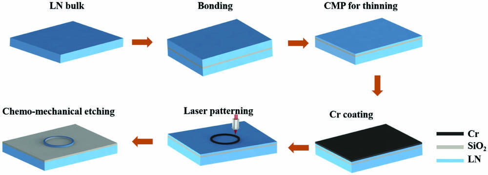
The manufacturing process for fabricating the LN microrings by CMP is schematically illustrated in Fig. 1, which mainly consists of two consecutive procedures including production of monocrystalline high-quality LN thin-film wafers and nanostructuring of LNOI microrings. To fabricate such LNOI microrings, first, an X-cut LN crystal was bonded to a silica buffer layer at room temperature, where the silica layer with a thickness of 2 µm was deposited on another LN bulk crystal by plasma enhanced chemical vapor deposition. Then, high-temperature annealing at 500°C was performed to enhance the bonding strength. Second, the top bulk crystal was thinned into a 4-µm-thick thin film via CMP, considering the trade-off between the surface evenness and thickness, as shown in Ref. [38]. Thus, combined with the techniques of step 1 and step 2, an LNOI thin-film wafer was formed. Third, to pattern the LN thin film into microrings by CMP etching, a 600-nm-thick chromium (Cr) layer was coated on the LNOI wafer by magnetron sputtering. Fourth, the Cr layer was ablated into a microring-pattern hard mask by femtosecond laser direct writing with a scan speed of 10 cm/s and a pulse width of 190 fs. The laser focal spot was approximately 1 µm, and the thickness of the ablation layer was controlled to be as small as 400 nm by choosing the average power of the laser. Fifth, the sample underwent CMP to etch the exposed LN thin film, leading to the pattern transferring from the Cr layer to LN thin film[
![]()
Figure 1.Illustration of the fabrication flow of the microrings.
3. Characteristics of LN Microrings
The optical microscope image and the magnified scanning-electron-microscope (SEM) image of the microrings are shown in Figs. 2(a) and 2(b), respectively, indicating the LN microring with a diameter of 200 µm and an ultra-smooth surface. To accurately measure the wedge angle and the height of the microrings, a small slit is cut through the microring with a focused ion beam, as shown in Fig. 2(c), showing a wedge angle of 9° and a height of 720 nm. Interestingly, the small wedge angle will drive the modes far from the edge of the microrings, benefiting higher
![]()
Figure 2.(a) Optical microscope image of the fabricated microring. (b) Magnified scanning-electron-microscope (SEM) image of the fabricated microring. (c) The SEM image shows that a small slit is cut through the microring with a focused ion beam. (d) The optical microscope image of the ridge waveguide on other LNOI chips for coupling of the microring.
To couple light into and out of the microring, a ridge waveguide with top width, bottom width, and height of 2.11 µm, 9.68 µm, and 700 nm, respectively, is fabricated on a second LNOI wafer (produced by ion slicing) by CMP etching, as shown in Fig. 2(d). The experimental setup is schematically illustrated in Fig. 3(a). The ridge waveguide was adjusted to be parallel with the top surface of the microrings by an
![]()
Figure 3.(a) Experimental setup for mode characterization. (b) Optical micrograph of the waveguide coupled with the microring. (c) The measured transmission spectrum. (d) and (e) Q factors of the modes fitted by Lorentz-shape curves; insets: the corresponding field distributions of the modes, where the direction presents the radial direction.
Figure 3(c) shows the transmission spectra of the microring at the wavelength ranging from 1566 nm to 1570 nm, exhibiting two sets of high-order transverse electric (TE) and transverse magnetic (TM) modes. The modes were simulated by a finite-element method[
4. Conclusion
In conclusion, we demonstrate an ultra-high
References
[1] J. Lin, F. Bo, Y. Cheng, J. Xu. Advances in on-chip photonic devices based on lithium niobate on insulator. Photon. Res., 8, 1910(2020).
[2] Y. Qi, Y. Li. Integrated lithium niobate photonics. Nanophotonics, 9, 1287(2020).
[3] Y. Kong, F. Bo, W. Wang, D. Zheng, H. Liu, G. Zhang, R. Rupp, J. Xu. Recent progress in lithium niobate: optical damage, defect simulation, and on-chip devices. Adv. Mater., 32, 1806452(2020).
[4] Y. Jia, L. Wang, F. Chen. Ion-cut lithium niobate on insulator technology: recent advances and perspectives. Appl. Phys. Rev., 8, 011307(2021).
[5] Y. Zheng, X. Chen. Nonlinear wave mixing in lithium niobate thin film. Adv. Phys. X, 6, 1889402(2021).
[6] J. Wang, F. Bo, S. Wan, W. Li, F. Gao, J. Li, G. Zhang, J. Xu. High-Q lithium niobate microdisk resonators on a chip for efficient electro-optic modulation. Opt. Express, 23, 23072(2015).
[7] G. Li, Y. Chen, H. Jiang, X. Chen. Broadband sum-frequency generation using d33 in periodically poled LiNbO3 thin film in the telecommunications band. Opt. Lett., 42, 939(2017).
[8] C. Wang, M. Zhang, X. Chen, M. Bertrand, A. Shams-Ansari, S. Chandrasekhar, P. Winzer, M. Loncar. Integrated lithium niobate electro-optic modulators operating at CMOS-compatible voltages. Nature, 562, 101(2018).
[9] Y. He, Q.-F. Yang, J. W. Ling, R. Luo, H. X. Liang, M. X. Li, B. Q. Shen, H. M. Wang, K. Vahala, Q. Lin. Self-starting bi-chromatic LiNbO3 soliton microcomb. Optica, 6, 1138(2019).
[10] C. Wang, M. Zhang, M. J. Yu, R. R. Zhu, H. Hu, M. Loncar. Monolithic lithium niobate photonic circuits for Kerr frequency comb generation and modulation. Nat. Commun., 10, 978(2019).
[11] B. Mu, X. Wu, Y. Niu, Y. Chen, X. Cai, Y. Gong, Z. Xie, X. Hu, S. Zhu. Locally periodically poled LNOI ridge waveguide for second harmonic generation. Chin. Opt. Lett., 19, 060007(2021).
[12] J. Lin, N. Yao, Z. Hao, J. Zhang, W. Mao, M. Wang, W. Chu, R. Wu, Z. Fang, L. Qiao, W. Fang, F. Bo, Y. Cheng. Broadband quasi-phase-matched harmonic generation in an on-chip monocrystalline lithium niobate microdisk resonator. Phys. Rev. Lett., 122, 173903(2019).
[13] Y. Li, Z. Huang, W. Qiu, J. Dong, H. Guan, H. Lu. Recent progress of second harmonic generation based on thin film lithium niobate. Chin. Opt. Lett., 19, 060012(2021).
[14] A. Rao, K. Abdelsalam, T. Aardema, A. Honardoost, G. F. Camacho-Gonzalez, S. Fathpour. Actively-monitored periodic-poling in thin-film lithium niobate photonic waveguides with ultrahigh nonlinear conversion efficiency of 4600 %W−1cm−2. Opt. Express, 27, 25920(2019).
[15] K. Zhang, Z. Chen, H. Feng, W.-H. Wong, E. Y.-B. Pun, C. Wang. High-Q lithium niobate microring resonators using lift-off metallic masks. Chin. Opt. Lett., 19, 060010(2021).
[16] J. Lu, J. Surya, X. Liu, Y. Xu, H. X. Tang. Octave-spanning supercontinuum generation in nanoscale lithium niobate waveguides. Opt. Lett., 44, 1492(2019).
[17] Y. Jia, Y. Ren, X. Zhao, F. Chen. “Surface lattice resonances in dielectric metasurfaces for enhanced light-matter interaction. Chin. Opt. Lett., 19, 060013(2021).
[18] J. Zhao, C. Ma, M. Ruesing, S. Y. Mookherjea. High quality entangled photon pair generation in periodically poled thin-film lithium niobate waveguides. Phys. Rev. Lett., 124, 163603(2020).
[19] G.-T. Xue, Y.-F. Niu, X. Y. Liu, J.-C. Duan, W. J. Chen, Y. Pan, K. P. Jia, X. H. Wang, H.-Y. Liu, Y. Zhang, P. Xu, G. Zhao, X. L. Cai, Y.-X. Gong, X. P. Hu, Z. D. Xie, S. N. Zhu. Ultrabright multiplexed energy-time-entangled photon generation from lithium niobate on insulator chip. Phys. Rev. Appl., 15, 064059(2021).
[20] B. Fang, S. Gao, Z. Wang, S. Zhu, T. Li. Efficient second harmonic generation in silicon covered lithium niobate waveguides. Chin. Opt. Lett., 19, 060004(2021).
[21] M. Xu, M. He, H. Zhang, J. Jian, Y. Pan, X. Liu, L. Chen, X. Meng, H. Chen, Z. Li, X. Xiao, S. Yu, S. Yu, X. Cai. High-performance coherent optical modulators based on thin-film lithium niobate platform. Nat. Commun., 11, 3911(2020).
[22] Y. F. Niu, C. Lin, X. Y. Liu, Y. Chen, X. P. Hu, Y. Zhang, X. L. Cai, Y.-X. Gong, Z. D. Xie, S. N. Zhu. Optimizing the efficiency of a periodically poled LNOI waveguide using in situ monitoring of the ferroelectric domains. Appl. Phys. Lett., 116, 101104(2020).
[23] Z. J. Yu, Y. Y. Tong, H. K. Tsang, X. K. Sun. High-dimensional communication on etchless lithium niobate platform with photonic bound states in the continuum. Nat. Commun., 11, 2602(2020).
[24] M. Zhang, C. Wang, R. Cheng, A. Shams-Ansari, M. Loncar. Monolithic ultra-high-Q lithium niobate microring resonator. Optica, 4, 1536(2017).
[25] R. B. Wu, M. Wang, J. Xu, J. Qi, W. Chu, Z. W. Fang, J. H. Zhang, J. X. Zhou, L. L. Qiao, Z. F. Chai, J. T. Lin, Y. Cheng. Long low-loss-lithium niobate on insulator waveguides with sub-nanometer surface roughness. Nanomaterials, 8, 910(2018).
[26] R. Wolf, I. Breunig, H. Zappe, K. Buse. Scattering-loss reduction of ridge waveguides by sidewall polishing. Opt. Express, 26, 19815(2018).
[27] J. T. Lin, J. X. Zhou, R. B. Wu, M. Wang, Z. W. Fang, W. Chu, J. H. Zhang, L. L. Qiao, Y. Cheng. High-precision propagation-loss measurement of single-mode optical waveguides on lithium niobate on insulator. Micromachines, 10, 612(2019).
[28] J. X. Zhou, R. H. Gao, J. T. Lin, M. Wang, W. Chu, W. B. Li, D. F. Yin, L. Deng, Z. W. Fang, J. H. Zhang, R. B. Wu, Y. Cheng. Electro-optically switchable optical true delay lines of meter-scale lengths fabricated on lithium niobate on insulator using photolithography assisted chemo-mechanical etching. Chin. Phys. Lett., 37, 084201(2020).
[29] P. Rabiei, W. H. Steier. Lithium niobate ridge waveguides and modulators fabricated using smart guide. Appl. Phys. Lett., 86, 161115(2005).
[30] H. Hu, J. Yang, L. Gui, W. Sohler. Lithium niobate-on-insulator (LNOI): status and perspectives. Proc. SPIE, 8431, 84311D(2012).
[31] R. Takigawa, E. Higurashi, T. Kawanishi, T. Asano. Lithium niobate ridged waveguides with smooth vertical sidewalls fabricated by an ultra-precision cutting method. Opt. Express, 22, 27733(2014).
[32] M. F. Volk, S. Suntsov, C. E. Rueter, D. Kip. Low loss ridge waveguides in lithium niobate thin films by optical grade diamond blade dicing. Opt. Express, 24, 1386(2016).
[33] T. Ding, Y. Zheng, X. Chen. Integration of cascaded electro-optic and nonlinear processes on a lithium niobate on insulator chip. Opt. Lett., 44, 1524(2019).
[34] M. Wang, R. Wu, J. Lin, J. Zhang, Z. Fang, Z. Chai, Y. Cheng. Chemo-mechanical polish lithography: a pathway to lowloss large-scale photonic integration on lithium niobateon insulator. Quantum Eng., 1, e9(2019).
[35] J. Zhang, Z. Fang, J. Lin, J. Zhou, M. Wang, R. Wu, R. Gao, Y. Cheng. Fabrication of crystalline microresonators of high quality factors with a controllable wedge angle on lithium niobate on insulator. Nanomaterials, 9, 1218(2019).
[36] V. S. Ilchenko, A. A. Savchenkov, A. B. Matsko, L. Maleki. Nonlinear optics and crystalline whispering gallery mode cavities. Phys. Rev. Lett., 92, 043903(2004).
[37] P. Rabiei, P. Gunter. Optical and electro-optical properties of submicrometer lithium niobate slab waveguides prepared by crystal ion slicing and wafer bonding. Appl. Phys. Lett., 85, 4603(2004).
[38] R. Gao, H. Zhang, F. Bo, W. Fang, Z. Hao, N. Yao, J. Lin, J. Guan, L. Deng, M. Wang, L. Qiao, Y. Cheng. Broadband highly efficient nonlinear optical processes in on-chip integrated lithium niobate microdisk resonators of Q factor above 108(2021).
[39] R. Wu, J. Zhang, N. Yao, W. Fang, L. L. Qiao, Z. Chai, J. Lin, Y. Cheng. Lithium niobate micro-disk resonators of quality factors above 107. Opt. Lett., 43, 4116(2018).
[40] H. Lee, T. Chen, J. Li, K. Y. Yang, S. Jeon, O. Painter, K. J. Vahala. Chemically etched ultra high-Q wedge-resonator on a silicon chip. Nat. Photon., 6, 369(2012).
[41] J. Zhang, R. Wu, M. Wang, Z. Fang, J. Lin, J. Zhou, R. Gao, W. Chu, Y. Cheng. High-index-contrast single-mode optical waveguides fabricated on lithium niobate by photolithography assisted chemo-mechanical etching (PLACE). Jpn. J. Appl. Phys., 59, 086503(2020).
[42] M. Oxborrow. Traceable 2-D finite-element simulation of the whispering-gallery modes of axisymmetric electromagnetic resonators. IEEE Trans. Microwave Theory Tech., 55, 1209(2007).
[43] J. Lin, Y. Xu, J. Ni, M. Wang, Z. Fang, L. Qiao, W. Fang, Y. Cheng. Phase-matched second harmonic generation in an on-chip LiNbO3 microresonator. Phys. Rev. Appl., 6, 014002(2016).
[44] D. E. Zelmon, D. L. Small, D. Jundt. Infrared corrected Sellmeier coefficients for congruently grown lithium niobate and 5 mol.% magnesium oxide-doped lithium niobate. J. Opt. Soc. Am. B, 14, 3319(1997).
[45] J. Zhang, R. Wu, M. Wang, Y. Liang, J. Zhou, M. Wu, Z. Fang, W. Chu, Y. Cheng. An ultra-high-Q lithium niobate microresonator integrated with a silicon nitride waveguide in the vertical configuration for evanescent light coupling. Micromachines, 12, 235(2021).
[46] K. Y. Yang, D. Y. Oh, S. H. Lee, Q.-F. Yang, X. Yi, B. Shen, H. Wang, K. Vahala. Bridging ultrahigh-Q devices and photonic circuits. Nat. Photon., 12, 297(2018).


Set citation alerts for the article
Please enter your email address

© Copyright 2018-2021 | Chinese Laser Press. All Rights Reserved 沪ICP备15018463号-20