• Photonics Research
  • Vol. 11, Issue 10, 1667 (2023)
Min Zhou1、2、†, Yukun Zhao1、2、4、†,*, Xiushuo Gu1, Qianyi Zhang1, Jianya Zhang3, Min Jiang1、2, and Shulong Lu1、2、5、*
Author Affiliations
  • 1Key Laboratory of Nanodevices and Applications, Suzhou Institute of Nano-Tech and Nano-Bionics (SINANO), Chinese Academy of Sciences (CAS), Suzhou 215123, China
  • 2School of Nano-Tech and Nano-Bionics, University of Science and Technology of China, Hefei 230026, China
  • 3Jiangsu Key Laboratory of Micro and Nano Heat Fluid Flow Technology and Energy Application, School of Physical Science and Technology, Suzhou University of Science and Technology, Suzhou 215009, China
  • 4e-mail: ykzhao2017@sinano.ac.cn
  • 5e-mail: sllu2008@sinano.ac.cn
  • show less
    DOI: 10.1364/PRJ.487936 Cite this Article Set citation alerts
    Min Zhou, Yukun Zhao, Xiushuo Gu, Qianyi Zhang, Jianya Zhang, Min Jiang, Shulong Lu. Light-stimulated low-power artificial synapse based on a single GaN nanowire for neuromorphic computing[J]. Photonics Research, 2023, 11(10): 1667 Copy Citation Text show less
    (a) Grow the GaN NWs on Si substrate. (b) Transfer the NWs onto the Si/SiO2 substrate. (c) Spin coat photoresist and fabricate the electrode patterns by electron beam lithography. (d) Fabricate the metal electrodes at both NW ends. (e) Schematic diagram of a biological synapse connecting two adjacent neurons. (f) Schematic illustration of the biological synapse. (g) Top-view and side-view SEM images of the GaN NWs. (h) PL curve of the GaN NWs. (i) Top-view SEM image of the single-GaN-NW synaptic device.
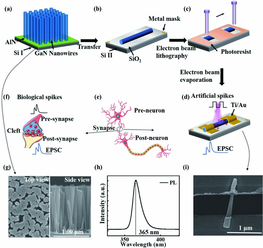
    Fig. 1. (a) Grow the GaN NWs on Si substrate. (b) Transfer the NWs onto the Si/SiO2 substrate. (c) Spin coat photoresist and fabricate the electrode patterns by electron beam lithography. (d) Fabricate the metal electrodes at both NW ends. (e) Schematic diagram of a biological synapse connecting two adjacent neurons. (f) Schematic illustration of the biological synapse. (g) Top-view and side-view SEM images of the GaN NWs. (h) PL curve of the GaN NWs. (i) Top-view SEM image of the single-GaN-NW synaptic device.
    (a) Full-scan XPS spectrum of the GaN NWs. Narrow-scan XPS spectra of (b) N 1s, (c) Ga 3d, and (d) O 1s elements within GaN NWs.
    Fig. 2. (a) Full-scan XPS spectrum of the GaN NWs. Narrow-scan XPS spectra of (b) N 1s, (c) Ga 3d, and (d) O 1s elements within GaN NWs.
    (a) STEM image and (b) high-resolution EDX mapping of the NW top. (c) AC-STEM image of the atomic model of top NW crystals. (d) STEM image and (e) high-resolution EDX mapping of the NW sidewall. (f) AC-STEM image of the atomic model of NW sidewall crystals. (g) Side-view STEM image and (h) EDX spectrum of the GaN NW.
    Fig. 3. (a) STEM image and (b) high-resolution EDX mapping of the NW top. (c) AC-STEM image of the atomic model of top NW crystals. (d) STEM image and (e) high-resolution EDX mapping of the NW sidewall. (f) AC-STEM image of the atomic model of NW sidewall crystals. (g) Side-view STEM image and (h) EDX spectrum of the GaN NW.
    (a) Schematic illustration of the stimulation processes in a biological synapse. EPSC of the single-GaN-NW synaptic device triggered by (b) two consecutive pulses and (c) multiple consecutive pulses. Light power intensity and operating bias of the device are 6.11 mW cm−2 and 5 V, respectively.
    Fig. 4. (a) Schematic illustration of the stimulation processes in a biological synapse. EPSC of the single-GaN-NW synaptic device triggered by (b) two consecutive pulses and (c) multiple consecutive pulses. Light power intensity and operating bias of the device are 6.11  mWcm2 and 5 V, respectively.
    (a) EPSC curves and (b) extracted results of the single-GaN-NW synaptic device under illumination with different incident light power densities. The light wavelength is 365 nm, and the operating bias of the device is 5 V. (c) Decay time constant of STM-to-LTM transition induced by different light intensities. (d) Responsivity of single GaN NW under 365 nm illumination at different biases (1–5 V). (e) EPSC curves and (f) extracted results of the single-GaN-NW synaptic device under illumination with different time intervals. The light pulse width is fixed as 500 ms. The light power intensity is 6.11 mW cm−2, and the operating bias of device is 5 V.
    Fig. 5. (a) EPSC curves and (b) extracted results of the single-GaN-NW synaptic device under illumination with different incident light power densities. The light wavelength is 365 nm, and the operating bias of the device is 5 V. (c) Decay time constant of STM-to-LTM transition induced by different light intensities. (d) Responsivity of single GaN NW under 365 nm illumination at different biases (1–5 V). (e) EPSC curves and (f) extracted results of the single-GaN-NW synaptic device under illumination with different time intervals. The light pulse width is fixed as 500 ms. The light power intensity is 6.11  mWcm2, and the operating bias of device is 5 V.
    EPSC of the synaptic device under illumination of light pulses. The light power intensity is 6.11 mW cm−2.
    Fig. 6. EPSC of the synaptic device under illumination of light pulses. The light power intensity is 6.11  mWcm2.
    (a) Equivalent circuit model and (b) I–V curve of the artificial synaptic device based on a single GaN NW. Schematic energy band diagrams of the single GaN NW (c) in dark, (d) under the first light stimulation, (e) without light stimulation, and (f) under the second light stimulation. (g) Learning experience of the artificial synaptic device.
    Fig. 7. (a) Equivalent circuit model and (b) I–V curve of the artificial synaptic device based on a single GaN NW. Schematic energy band diagrams of the single GaN NW (c) in dark, (d) under the first light stimulation, (e) without light stimulation, and (f) under the second light stimulation. (g) Learning experience of the artificial synaptic device.
    (a) Schematic illustration of ANN simulation using 784 input neurons and 10 output neurons, connected by 784×100×10 synaptic weights. (b) Experimental data and fitted curves of LTP/LTD characteristics triggered by light pulses. During the measurements of LTP and LTD data, the light power intensity and bias voltage are 6.59 mW cm−2 and 5 V, respectively. (c) Recognition results of the randomly selected numbers from the MNIST database. (d) Recognition accuracy versus training epoch in the simulation.
    Fig. 8. (a) Schematic illustration of ANN simulation using 784 input neurons and 10 output neurons, connected by 784×100×10 synaptic weights. (b) Experimental data and fitted curves of LTP/LTD characteristics triggered by light pulses. During the measurements of LTP and LTD data, the light power intensity and bias voltage are 6.59  mWcm2 and 5 V, respectively. (c) Recognition results of the randomly selected numbers from the MNIST database. (d) Recognition accuracy versus training epoch in the simulation.
    MaterialsStructureVoltage (V)Pulse Width (ms)Energy Consumption (pJ)Reference
    TiO2NW1050130[53]
    InGaAsNW0.000111.78×103[54]
    ZnONW110001×106[28]
    SiNW1501000[55]
    InAsNW0.5212.5[52]
    GaNFilm0.01100033.4[11]
    GaNMW//500[56]
    GaNNW510002.72This work
    Table 1. Comparison between This Work and Some State-of-the-Art Synaptic Devices with the Same Structure or Material
    Min Zhou, Yukun Zhao, Xiushuo Gu, Qianyi Zhang, Jianya Zhang, Min Jiang, Shulong Lu. Light-stimulated low-power artificial synapse based on a single GaN nanowire for neuromorphic computing[J]. Photonics Research, 2023, 11(10): 1667
    Download Citation