1Key Laboratory of Nanodevices and Applications, Suzhou Institute of Nano-Tech and Nano-Bionics (SINANO), Chinese Academy of Sciences (CAS), Suzhou 215123, China
2School of Nano-Tech and Nano-Bionics, University of Science and Technology of China, Hefei 230026, China
3Jiangsu Key Laboratory of Micro and Nano Heat Fluid Flow Technology and Energy Application, School of Physical Science and Technology, Suzhou University of Science and Technology, Suzhou 215009, China
Min Zhou, Yukun Zhao, Xiushuo Gu, Qianyi Zhang, Jianya Zhang, Min Jiang, Shulong Lu, "Light-stimulated low-power artificial synapse based on a single GaN nanowire for neuromorphic computing," Photonics Res. 11, 1667 (2023)
Copy Citation Text
The fast development of the brain-inspired neuromorphic computing system has ignited an urgent demand for artificial synapses with low power consumption. In this work, it is the first time a light-stimulated low-power synaptic device based on a single GaN nanowire has been demonstrated successfully. In such an artificial synaptic device, the incident light, the electrodes, and the light-generated carriers play the roles of action potential, presynaptic/postsynaptic membrane, and neurotransmitter in a biological synapse, respectively. Compared to those of other synaptic devices based on GaN materials, the energy consumption of the single-GaN-nanowire synaptic device can be reduced by more than 92%, reaching only . It is proposed that the oxygen element can contribute to the synaptic characteristics by taking the place of the nitrogen site. Moreover, it is found that the dynamic “learning-forgetting” performance of the artificial synapse can resemble the behavior of the human brain, where less time is required to relearn the missing information previously memorized and the memories can be strengthened after relearning. Based on the experimental conductance for long-term potentiation (LTP) and long-term depression (LTD), the simulated network can achieve a high recognition rate up to 90% after only three training epochs. Such few training times can reduce the energy consumption in the supervised learning processes substantially. Therefore, this work paves an effective way for developing single-nanowire-based synapses in the fields of artificial intelligence systems and neuromorphic computing technology requiring low-power consumption.
1. INTRODUCTION
Currently, neural networks play an important role in deep learning by processing text, audio, and video data sequences [1]. Due to the separate processor and memory units, von Neumann architecture-based computing systems are encountering fundamental physical limitations of energy consumption and access speed [2,3], which makes it difficult to meet the requirements of the rapid development of artificial intelligence, big data, and Internet of Things. In general, the human brain has one of the most sophisticated structures, which can process and store large quantities of data with high speed and low power consumption simultaneously [4,5]. Meanwhile, the emerging neuromorphic computing has the advantages of high efficiency, low power consumption, and flexible adaptive ability, which can meet the needs of simulating neural brain systems [6,7]. Furthermore, the light-stimulated synaptic phototransistor has many outstanding characteristics, such as high anti-interference, high bandwidth, low cross talk, and low power consumption [8–12]. Therefore, light-stimulated neuromorphic devices with low power are essential and quite necessary for the development of neuromorphic computing.
In the human brain, almost neuron-synaptic junction units exist, which allow the brain to perform complex neural activities [12,13]. When the input is an optical signal, traditional synaptic devices need additional sensors for photoelectric conversion [14]. Thus, light-stimulated synapse devices are of great significance in simulating the human visual system, which receives and processes external information [15]. It is common for light-stimulated synaptic devices to contain active materials that are stimulus-history dependent, such as persistent photoconductivity (PPC) [11,16,17]. The varied conductivity or current variation can be utilized to emulate the functions of biological synapses under stimuli [11,16,17]. GaN-based materials with direct bandgaps have the great potential in the neuromorphic field for the following reasons. First, stable PPC effect can be observed in GaN materials at room temperature, paving the way for light-stimulated synaptic devices to be constructed [18,19]. Second, GaN-based materials are compatible with the present semiconductor technology, allowing for the large-scale manufacture of optoelectronic synaptic arrays [20]. Finally, GaN-based materials offer great potential for on-chip integration of optoelectronic neural morphological devices and light sources [11]. Hence, it is very promising to prepare GaN-based photonic synaptic devices.
In addition, one-dimensional (1D) materials, such as nanowires (NWs), have the analogous topology to tubular axons, which greatly influences the processing of data in biological systems [21]. Combined with the excellent characteristics of a large surface-to-volume ratio, efficient charge carrier transport, and effective light response to specific wave bands, these 1D materials can regulate synaptic activities more flexibly with a low power [22–26]. Although neuromorphic systems based on GaN-based NWs pave a new way to mimic the capability of human brain [27–30], GaN synaptic devices are normally based on thin films [two-dimensional (2D) material] [11,31]. Furthermore, they are mainly used for electrical synapses, not light-stimulated synapses [11,31]. In our previous work, we fabricated GaN-based NWs and utilized them in photodetectors successfully [32–35]. However, very few works have been reported on utilizing the single GaN NW in light-stimulated artificial synapses, not to mention realizing the performance of low power consumption.
Sign up for Photonics Research TOC. Get the latest issue of Photonics Research delivered right to you!Sign up now
In this work, we reported a light-stimulated synaptic device based on single GaN NW successfully. This artificial synapse is capable of emulating multiple functionalities of biological synapses, including the spike-duration dependence, light-intensity dependence, transition from short-term memory (STM) to long-term memory (LTM), and the learning behavior. The energy consumption of such synaptic device is demonstrated to be very low, reaching only . Apart from the experiments, the underlying mechanisms of the synaptic device have also been studied. In order to verify the learning ability of NW synaptic devices, an artificial neural network (ANN) for mimicking bio-vision has been established and demonstrated.
2. EXPERIMENTAL AND NUMERICAL METHODOLOGIES
A. Preparation Procedure of GaN NWs
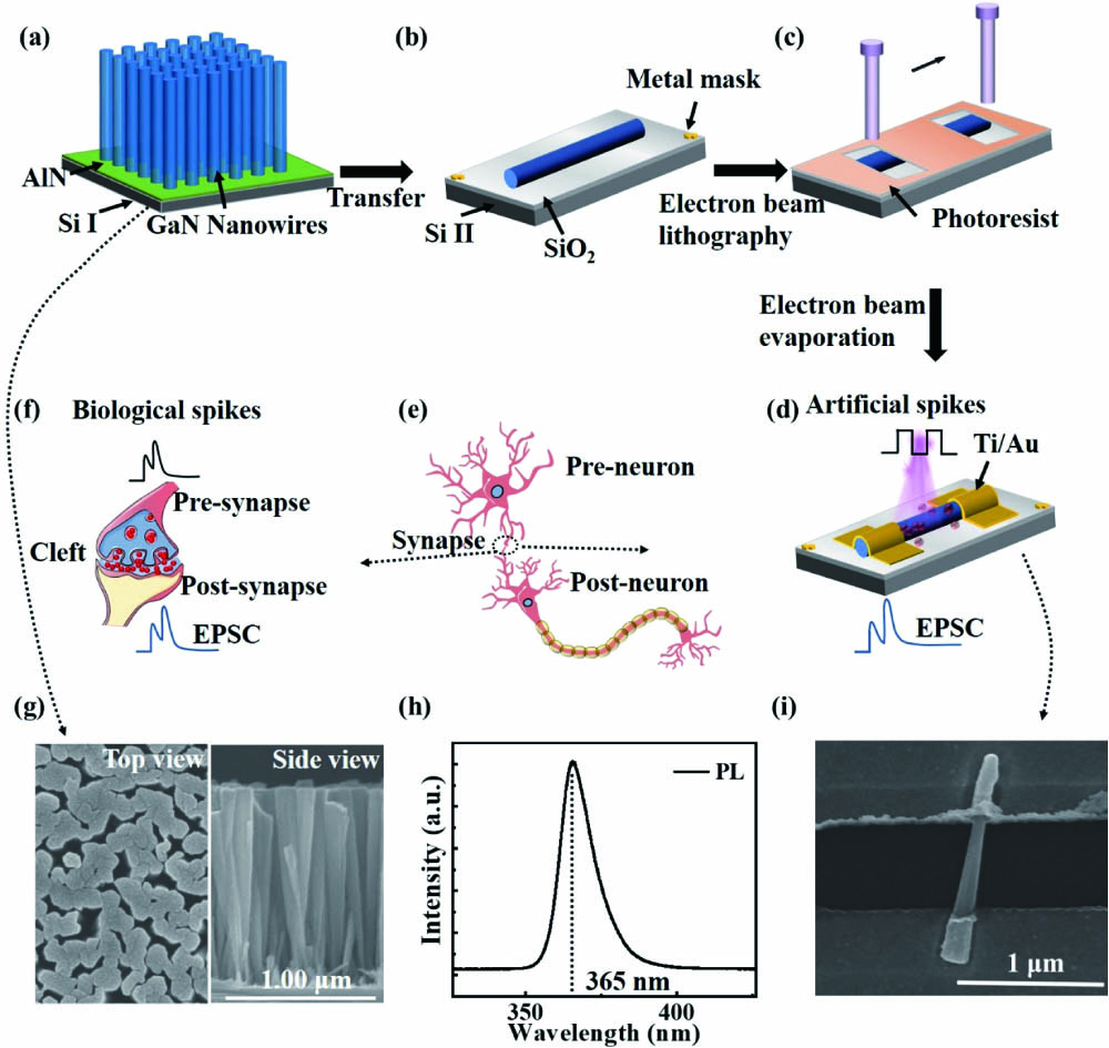
The GaN NWs [Fig. 1(a)] were grown on the -type Si (111) substrates by molecular beam epitaxy (MBE, Vecco G20). To eliminate native oxides in the growth chamber before epitaxial growth, the Si substrates were heated to 900°C for 15 min. The N atoms were supplied by the N plasma cell, while the Ga atoms were generated by the Ga effusion cell. First, GaN deposited on the Si surface forms into islands through the Stranski–Krastanow growth mode [36–38]. Due to strain minimization, these islands are expected to be preferential sites. In other words, the deposited GaN initially forms into islands, which act as a material collector and a seed for the NW growth [36–38]. After that, the GaN section was grown with a nominal Ga flux of for 300 min. During the epitaxial process, the plasma power and nitrogen flow rate were kept at 450 W and 4.8 sccm, respectively.
Figure 1.(a) Grow the GaN NWs on Si substrate. (b) Transfer the NWs onto the substrate. (c) Spin coat photoresist and fabricate the electrode patterns by electron beam lithography. (d) Fabricate the metal electrodes at both NW ends. (e) Schematic diagram of a biological synapse connecting two adjacent neurons. (f) Schematic illustration of the biological synapse. (g) Top-view and side-view SEM images of the GaN NWs. (h) PL curve of the GaN NWs. (i) Top-view SEM image of the single-GaN-NW synaptic device.
As shown in Fig. 1(b), the as-grown NW based on Si I substrate was transferred onto the top surface of the 280 nm layer under a stereoscopic microscope, which was on a foreign Si II substrate. Several cross markings were fabricated by the photolithography on the layer before transferring NW. Then scanning electron microscopy (SEM, S-4800) was utilized to determine the position of single NW by the cross markings. After that, the photoresist was spin-coated. Then electron beam lithography (EBL) technology was used to form electrode patterns at both ends of the positioned single NW [Fig. 1(c)]. Finally, the metal electrodes of Ti/Au (20/60 nm) were prepared at both NW ends by electron beam evaporation and lift-off processes [Fig. 1(d)].
C. Characterization and Measurements
In this work, SEM (S-4800) was utilized to characterize the morphology and position of NWs. Aberration-corrected scanning transmission electron microscopy (AC-STEM) and high-resolution energy-dispersive X-ray (EDX) mapping were operated to measure the morphology and element distribution of NWs. Current–voltage (I–V) characteristics were measured using an Agilent B1505A semiconductor parameter analyzer. During the response measurements, the 365 nm LED was used as the light source, which was controlled by a function generator (FY6900-20M). To characterize the optical properties, a photoluminescence (PL, SP2500i) system with a 325 nm laser was utilized. X-ray photoelectron spectroscopy (XPS, PHI 5000 Versaprobe III, ULVAC-PHI) was carried out to characterize the chemical states and atomic binding states of the NWs.
D. Neuromorphic Simulation
A multilayer perceptron (MLP) neural network model was set up based on the experimental results of device parameters, such as the nonlinear values. Each synaptic device acts as a neuron in the neural network. The Modified National Institute of Standards and Technology (MNIST) dataset was used for input. The image pixel information is , corresponding to 784 input neurons [39]. The output of 10 classes of digits (0–9) could be converted into one pot vector for recognition, such as . In this model, the sigmoid function was used as the activation function. The random gradient descent method was used as the optimization algorithm to continuously iterate and optimize the weight value [40]. Furthermore, the backpropagation algorithm was used to continuously adjust the weight value and threshold value of the network, so as to minimize the total square error and update the weight value in real time [41]. Finally, the evaluation function was used to convert the one pot vector into numbers. By evaluating and predicting the correct numbers, the MNIST handwritten dataset could complete the number recognition.
3. RESULTS AND DISCUSSION
A. Characterization of GaN Nanowires
In the biological nervous system, the signal transmission between adjacent neurons is completed by synapses [Figs. 1(e) and 1(f)], which are composed of presynapse, postsynapse, and synaptic cleft [40]. In this work, the structure of NW optoelectronic synaptic device is proposed to be similar to that of biological synapses [Figs. 1(d)–1(f)]. As illustrated in Fig. 1(g), the grown NWs show a good verticality and uniformity. The heights of the NWs are over 1300 nm, and the diameter ranges from 60 nm to 120 nm. Figure 1(h) shows the PL peak centers at , corresponding to the GaN characteristic peak. Furthermore, the device structure of the single-NW-based synapse was successfully fabricated without any obvious fractures [Fig. 1(i)]. According to Figs. 1(d) and 1(i), the structure of the single-NW-based synapse is consistent with the design. In such an artificial synaptic device, the incident light, the electrodes, and the light-generated carriers play the roles of action potential, presynaptic/postsynaptic membrane, and neurotransmitter, respectively. Moreover, when the device is applied by light stimulation, the collected current is regarded as excitatory postsynaptic current (EPSC), depending on the synaptic weight [42].
In addition, the XPS spectrum is utilized to determine the chemical characteristics and binding states of atoms present in GaN NWs. From Fig. 2(a), the entire XPS spectrum shows the expected constituent elements of Ga and N. The N 1s spectrum in Fig. 2(b) can be deconvoluted into three peaks. Among them, the peak at corresponds to the bonding of N–Ga, while the other two peaks at and correspond to Ga LMM Auger transitions [43]. As shown in Figs. 2(a), 2(c), and 2(d), the oxygen element exists, which is usually attributed to unintentional doping during the growth process and the oxidation of NW surface in air. However, the peak intensity of Ga–N is much higher than that of Ga–O [Fig. 2(c)], proving that GaN is the dominant material within the NWs.
Figure 2.(a) Full-scan XPS spectrum of the GaN NWs. Narrow-scan XPS spectra of (b) N 1s, (c) Ga 3d, and (d) O 1s elements within GaN NWs.
As shown in Fig. 3(a), the top of the GaN NW exhibits a small V-shaped pit (Region I) and an uneven surface (Region II). Figure 3(b) shows the presence of on the top surface. According to the atomic arrangement in Fig. 3(c), it is proposed that the amorphous can be produced on the surface of the GaN NW [44]. Moreover, Figs. 3(d)–3(f) reveal a distinct shell on the sidewall of the GaN NW. To ensure a more accurate analysis, the side-view STEM image on various NWs has been observed, which reveals the formation within the NWs [Fig. 3(g)]. According to the EDX spectrum shown in Fig. 3(h), the O intensity provides the evidence for the presence of oxygen vacancies [45]. The existence of oxygen vacancies can be a key reason contributing to the synaptic characteristics of devices [46].
Figure 3.(a) STEM image and (b) high-resolution EDX mapping of the NW top. (c) AC-STEM image of the atomic model of top NW crystals. (d) STEM image and (e) high-resolution EDX mapping of the NW sidewall. (f) AC-STEM image of the atomic model of NW sidewall crystals. (g) Side-view STEM image and (h) EDX spectrum of the GaN NW.
As illustrated in Fig. 4(a), when the biological presynapse is stimulated, the presynapse membrane will trigger the rapid release of neurotransmitters, including dopamine (Dopa) for excitatory response and acetylcholine (Ach) for memory formation [47]. Then the receptor of the postsynapse membrane opens the channel to realize signal transmission [I process in Fig. 4(a)] [28]. When the stimulation is removed, the neurotransmitter is rapidly degraded or recycled into the cell, resulting in closing the channel [II process in Fig. 4(a)]. When stimulated again, more neurotransmitters are bound to receptors, leading to open more channels and the higher signal transmission [III process in Fig. 4(a)]. During this process, the change of synaptic weight represents the degree of connectivity between neurons. The synaptic weight can be changed by adjusting the activity of presynaptic and postsynaptic neurons, which is commonly called synaptic plasticity [48]. As one of the important features of biological synapses, the synaptic plasticity lays the foundation for many functions in the human brain, such as learning, forgetting, and image recognition [49].
Figure 4.(a) Schematic illustration of the stimulation processes in a biological synapse. EPSC of the single-GaN-NW synaptic device triggered by (b) two consecutive pulses and (c) multiple consecutive pulses. Light power intensity and operating bias of the device are and 5 V, respectively.
From Fig. 4(b), EPSC is induced by two continuous light pulses with an interval of 1s. The second peak () is obviously larger than the first peak (). Thus, the current generated by the first optical pulse will not decay to the initial value before the arrival of the second optical pulse. In other words, when the second pulse is executed on the basis of the first pulse, the EPSC value can be greatly increased. The whole processes within the artificial synaptic device correspond to those within biological synapses [I, II, and III processes in Figs. 4(a) and 4(b)]. The increased EPSC caused by more carrier generation is similar to the dynamics of more influx in biological synapses [2]. Hence, such a single-GaN-NW synaptic device has the ability to simulate biological synapses. To study the short-term potentiation and long-term potentiation (LTP) of the device, the EPSC value of device was measured under more consecutive light pulses [Fig. 4(c), 25 light pulses with an interval of 5 s]. In general, an exponential decay is used to study the forgetting curve [47], where represents the current at the time of and represents the initial current. is a constant factor, and is the constant of decay time. From Figs. 4(b) and 4(c), is increased more than 20 times from 0.33 to 7.58 s triggered by more light pulses, demonstrating the existence of STM-to-LTM transition.
In biological systems, synaptic plasticity depends on the spike duration, frequency, and light intensity of the external environment. Inspired by biological synapses, the spike-duration dependence and light-intensity dependence of a single GaN NW are explored and shown in Fig. 5. When the power intensity of the stimulated light pulse increases from about 0.21 to , the EPSC gradually increases [Figs. 5(a) and 5(b)]. Hence, the maximum EPSC is dependent on the power intensity of the incident light pulse. Meanwhile, the data fitted by Eq. (1) increase from 3.6 to 7.2 s [Fig. 5(c)], strongly indicating the transfer from STM to LTM [50]. In addition, the responsivity of the single GaN NW under 365 nm illumination can be calculated using the following formula [34]:
and represent the saturation current under illumination and the dark current in the absence of light, respectively [32]. is the incident power intensity S represents the effective area in PD, which uses the area of single GaN NW facing the illumination (). From Fig. 5(d), it can be observed that the device exhibits a high responsivity (), which is primarily attributed to the small size of the single NW.
Figure 5.(a) EPSC curves and (b) extracted results of the single-GaN-NW synaptic device under illumination with different incident light power densities. The light wavelength is 365 nm, and the operating bias of the device is 5 V. (c) Decay time constant of STM-to-LTM transition induced by different light intensities. (d) Responsivity of single GaN NW under 365 nm illumination at different biases (1–5 V). (e) EPSC curves and (f) extracted results of the single-GaN-NW synaptic device under illumination with different time intervals. The light pulse width is fixed as 500 ms. The light power intensity is , and the operating bias of device is 5 V.
As clearly shown in Figs. 5(e) and 5(f), when the device is stimulated by the smaller time intervals (), the EPSC can be enhanced. When the next pulse is stimulated, the previous pulse has not returned to the initial state in time. The smaller the time interval is, the higher the starting point of current for the next light pulse. However, when is smaller than 200 ms, the EPSC tends to be saturated. This behavior is similar to biological PSC saturation, which is caused by postsynaptic receptor saturation interacting with limited presynaptic calcium flux [51].
C. Energy Consumption and Working Mechanism
Figure 6.EPSC of the synaptic device under illumination of light pulses. The light power intensity is .
In order to deeply understand the working mechanism of the optoelectronic synapse, an equivalent circuit model of the metal–semiconductor–metal () structure and energy band diagrams are plotted in Figs. 7(a)–7(f). As only the NW can absorb the photons and generate the carriers in the synaptic device, the main source of photocurrent contribution originates from the exposed NW [57]. electrode is applied the negative bias, while electrode is applied the positive bias [Fig. 7(a)]. In the structure, the performance of the device with Schottky contact [Fig. 7(b)] is mainly determined by the reverse-biased Schottky barrier (, ) [2]. Thus, to simplify the analyses, only contact is discussed here. Furthermore, the resistance before and after ultraviolet (UV) light irradiation is significantly reduced. The decrease of and could be the key factors contributing to the increase of current [2].
Figure 7.(a) Equivalent circuit model and (b) I–V curve of the artificial synaptic device based on a single GaN NW. Schematic energy band diagrams of the single GaN NW (c) in dark, (d) under the first light stimulation, (e) without light stimulation, and (f) under the second light stimulation. (g) Learning experience of the artificial synaptic device.
A Schottky contact is formed at the local contact (), and the defects within the NW are shown in Fig. 7(c) without illumination. When the device is stimulated by light pulses, the photogenerated carriers separate, and the reduction of is conducive to carrier transport [ in Fig. 7(d)]. Some photogenerated holes are captured by the oxygen vacancies (), forming quite stable complexes by the following equation [58]:
Such complexes make electron–hole () recombination more difficult, causing a portion of the photogenerated electrons to remain in the conduction band and contributing to the maintenance of the photocurrent even after the illumination is interrupted [Fig. 7(e)] [58]. When the light pulse is stimulated again [Fig. 7(f)], more photogenerated electrons and holes will be collected by the electrodes, generating a greater current than the last one, leading to the synaptic characteristics. The order of the values mentioned above is .
The learning process of a human typically takes place in a step-by-step manner. Unless the same information is acquired continuously over time, the information acquired and stored in temporary memory will initially decay. This process is consistent with Ebbinghaus’s forgetting curve, which further proves that the forgetting process of the human brain is a function of time [47]. In order to study the device in simulating the learning behavior of the human brain, the synaptic weight () is used to represent the memory level of the device, which is defined as the following equation [59]:
and are the initial current and the current after light stimulation ( is the number of light pulses), respectively. From Fig. 4, the device is found to have the characteristics of both STM (two light pulses) and LTM (21 light pulses). To simplify the measurement, a learning stage of presynaptic stimulation is defined to contain 21 light pulses [Fig. 7(g)]. In the first learning process, the synaptic weight is gradually increased. After removing the light stimulation, the synaptic weight gradually decreases to a certain level (first forgetting). In the subsequent learning process (second learning), by only 11 light pulses, the stimulated synaptic weight is able to reach the highest level achieved during the first learning process, which requires more (21) light pulses. Then, the synaptic weight continuously increases to a higher memory level. After the same time of 5 s for decaying, the synaptic weight of the second forgetting process keeps a higher level than the first decay. Similar phenomena can also be achieved in the third learning and forgetting processes. These dynamic “learning−forgetting” processes resemble the behavior of the human brain that less time is required to relearn the missing information previously memorized and the memories can be strengthened after relearning [8]. Therefore, the synaptic device based on a single GaN NW can functionally emulate this stepwise learning style in the human brain.
D. Number Recognition for Neuromorphic Computing
According to the instructions in NeuroSimV3.0 [60,61], a synaptic device based on a single GaN NW is employed to simulate ANNs used for pattern recognition. Meanwhile, the entire neural network can be operated by stimulating one synaptic device, which is based on the assumption that each neuron is the same in the ANNs [61]. As shown in Fig. 8(a), a three-layer perception neural model is adopted to perform supervised learning with the backpropagation algorithm and random gradient descent algorithm [62]. The handwritten digits are obtained from the MNIST database, which are divided into pixels corresponding to 784 input neurons [39]. The hidden layer consists of 100 neurons, and the output layer consists of 10 neurons corresponding to 10 digits ranging from 0 to 9 [28]. Among the connections of the neurons, the synaptic weights will eventually be saved through the calculation process of algorithms, which were extracted from the conductance of different potentiating and depressing states shown in Fig. 8(b) by the following equations [54,63]:
and are the conductance for LTP and long-term depression (LTD), respectively [54]. , , and are directly extracted from the experimental data, which represent the maximum conductance, minimum conductance, and maximum pulse number required to switch the device between the minimum and maximum conductance states [54]. is the parameter that controls the nonlinear behavior of the weight update. can be positive (blue) or negative (black) [54]. is simply a function of that fits the functions by , , and is the conductance after normalization. is the conductance value of the current state [54]. Using Eqs. (6)–(9), the nonlinear data of LTP and LTD are fitted to be 3.38 and , respectively [Fig. 8(b)]. By simulating ANN on the MNIST database, 20 samples are randomly selected in Fig. 8(c), while 10,000 samples are identified in Fig. 8(d). Most numbers can be identified accurately [Fig. 8(c)]. As clearly illustrated in Fig. 8(d), such a simulated network can achieve a high recognition rate up to 90% after only three training epochs. The recognition rate can be increased to 93% after 30 training epochs. Considering the requirement of low-power consumption of the synaptic devices, fewer training times can reduce the energy consumption in the supervised learning processes substantially. Hence, this single-GaN-NW synaptic device has the great application potential in neuromorphic computing technology.
Figure 8.(a) Schematic illustration of ANN simulation using 784 input neurons and 10 output neurons, connected by synaptic weights. (b) Experimental data and fitted curves of LTP/LTD characteristics triggered by light pulses. During the measurements of LTP and LTD data, the light power intensity and bias voltage are and 5 V, respectively. (c) Recognition results of the randomly selected numbers from the MNIST database. (d) Recognition accuracy versus training epoch in the simulation.
In this work, an artificial synaptic device based on a single GaN NW has been fabricated successfully, which exhibits the characteristics of spike-duration dependence and light-intensity dependence. Furthermore, the transition from STM to LTM and the human learning behavior are also emulated in this light-stimulated synaptic device. Furthermore, the energy consumption of the single-GaN-NW synaptic device can be as low as for a single synaptic event. Thanks to the dynamic “learning-forgetting” performance, the artificial synaptic device can resemble the brain-like behavior of less time being required to relearn the missing information previously memorized and strengthen memories after relearning. Simulation of a neural network utilizing the single-GaN-NW synapse is carried out, demonstrating a high recognition accuracy up to 93% after 30 training epochs. Hence, such an artificial synapse based on a single NW has great potential in a wide range of applications requiring low power consumption, such as the neuromorphic computing systems and bio-realistic artificial intelligence.
[60] P. Y. Chen, X. Peng, S. Yu. NeuroSim +: an integrated device-to-algorithm framework for benchmarking synaptic devices and array architectures. 63rd IEEE Annual International Electron Devices Meeting (IEDM), 6.1.1-6.1.4(2017).
Min Zhou, Yukun Zhao, Xiushuo Gu, Qianyi Zhang, Jianya Zhang, Min Jiang, Shulong Lu, "Light-stimulated low-power artificial synapse based on a single GaN nanowire for neuromorphic computing," Photonics Res. 11, 1667 (2023)