• Acta Optica Sinica
  • Vol. 41, Issue 1, 0131001 (2021)
Zhanshan Wang*, Qiushi Huang, Zhong Zhang, Shengzhen Yi, Wenbin Li, Zhengxiang Shen, Runze Qi, and Jun Yu
Author Affiliations
  • Key Laboratory of Advanced Micro-Structured Materials, Ministry of Education, Institute of Precision Optical Engineering, School of Physics Science and Engineering, Tongji University, Shanghai 200092, China
  • show less
    DOI: 10.3788/AOS202141.0131001 Cite this Article Set citation alerts
    Zhanshan Wang, Qiushi Huang, Zhong Zhang, Shengzhen Yi, Wenbin Li, Zhengxiang Shen, Runze Qi, Jun Yu. Extreme Ultraviolet, X-Ray and Neutron Thin Film Optical Components and Systems[J]. Acta Optica Sinica, 2021, 41(1): 0131001 Copy Citation Text show less
    Research fields of Institute of Precision Optics and Engineering (IPOE) in short wavelength optical components and systems
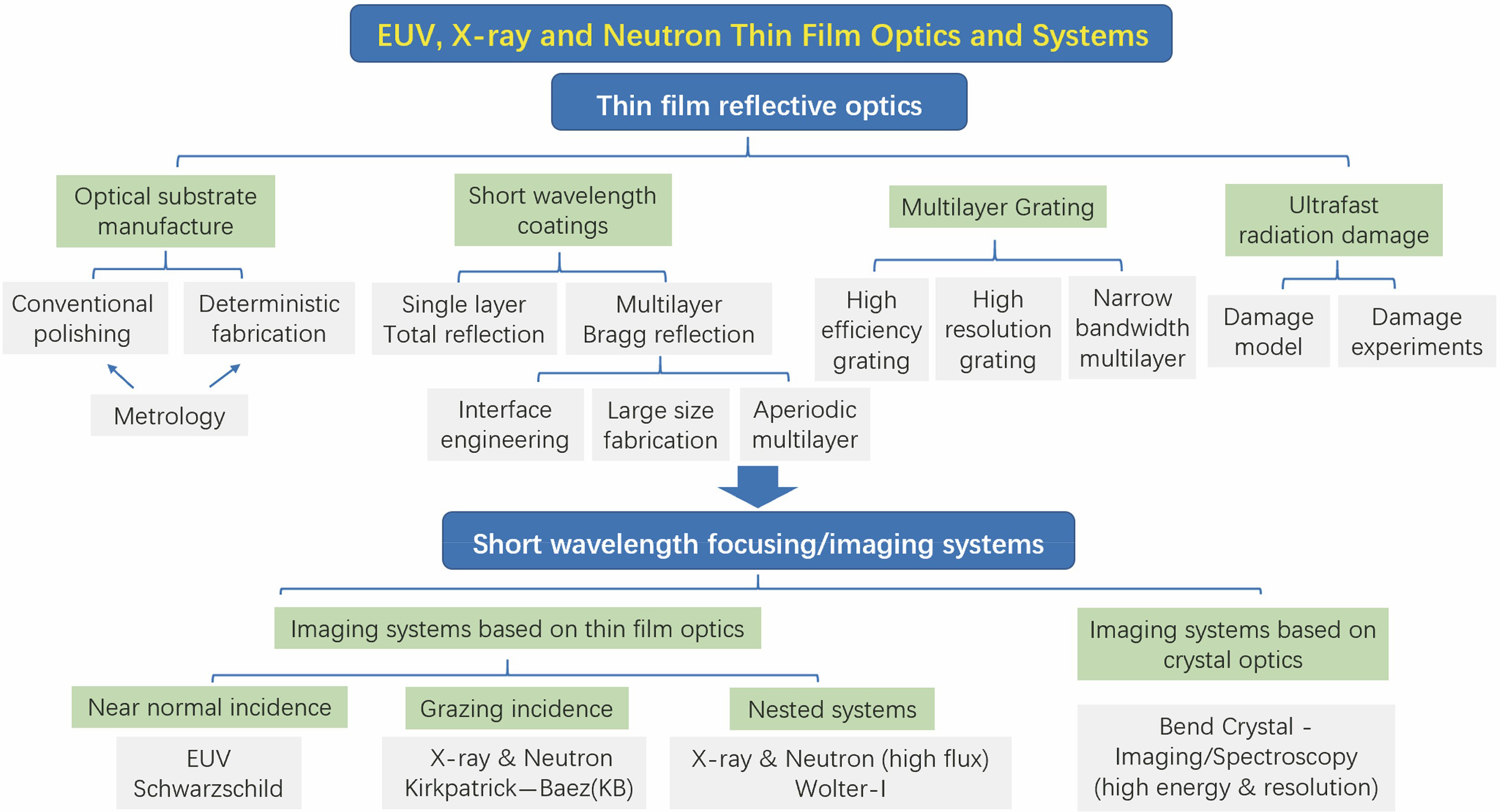
    Fig. 1. Research fields of Institute of Precision Optics and Engineering (IPOE) in short wavelength optical components and systems
    Polishing platform and machining results for large size mirrors. (a) Large size annular lapping machine in the laboratory; (b) measured figure result of a 200 mm-diameter quartz mirror based on annular lapping technology; (c) measured surface roughness of the mirror using optical profiler
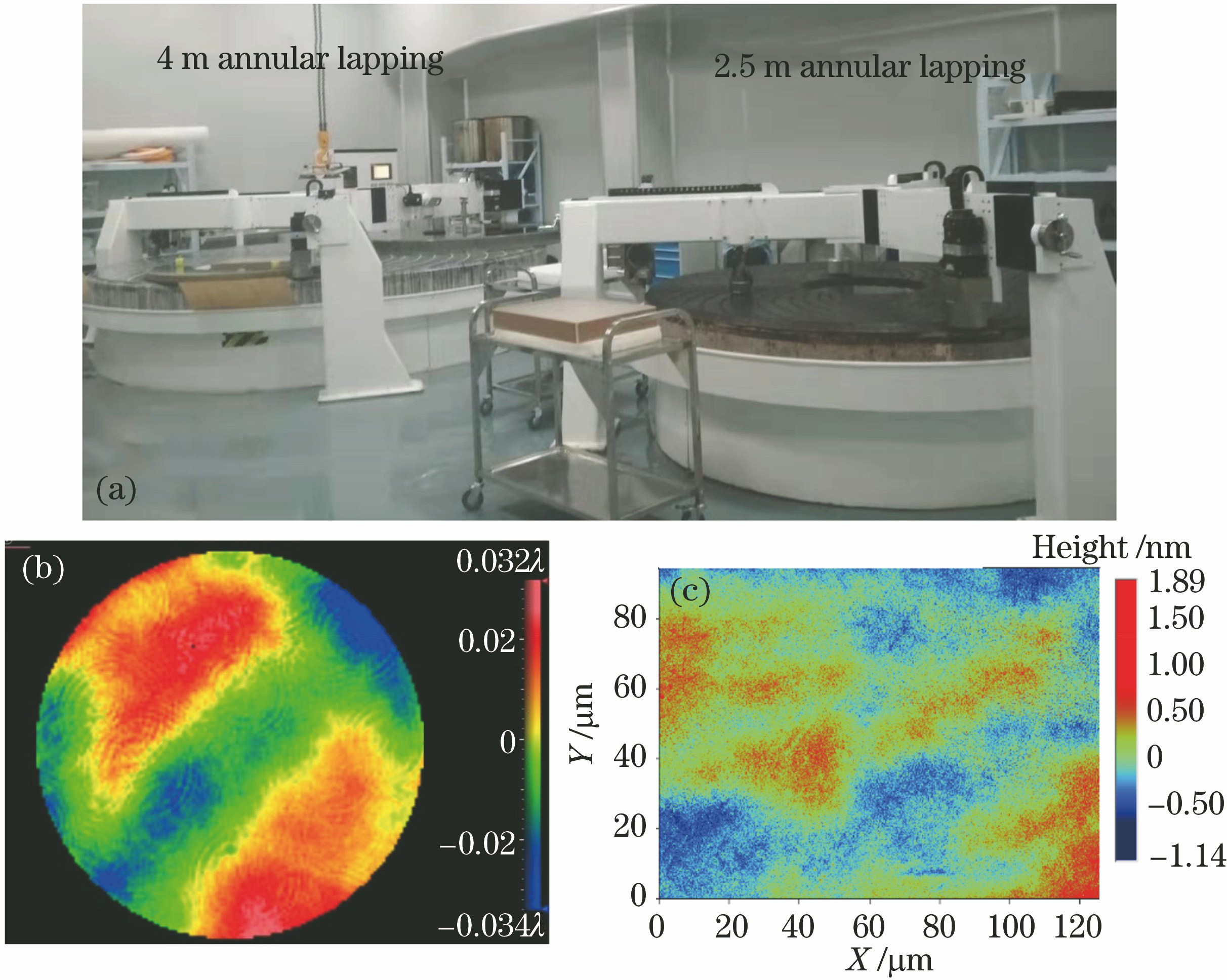
    Fig. 2. Polishing platform and machining results for large size mirrors. (a) Large size annular lapping machine in the laboratory; (b) measured figure result of a 200 mm-diameter quartz mirror based on annular lapping technology; (c) measured surface roughness of the mirror using optical profiler
    Measured results of the single crystalline Si mirror with 240 mm length after figure correction
    Fig. 3. Measured results of the single crystalline Si mirror with 240 mm length after figure correction
    Figure measurement results of an elliptical cylindrical mirror fabricated by profile coating. (a)Original figure of the elliptical cylindrical mirror; (b) residual figure error after removing the best-fit power
    Fig. 4. Figure measurement results of an elliptical cylindrical mirror fabricated by profile coating. (a)Original figure of the elliptical cylindrical mirror; (b) residual figure error after removing the best-fit power
    Full spatial frequency characterization platform components. (a) Laser interferometer; (b) contact-type profiler; (c) optical profiler; (d) atomic force microscope
    Fig. 5. Full spatial frequency characterization platform components. (a) Laser interferometer; (b) contact-type profiler; (c) optical profiler; (d) atomic force microscope
    Power spectral density curves of the Si thin film surface morphology[16]
    Fig. 6. Power spectral density curves of the Si thin film surface morphology[16]
    Algorithm-based stitching interferometry[18]. (a) Schematic of the stitching measurement procedures; (b) measurement repeatability error of spherical mirror
    Fig. 7. Algorithm-based stitching interferometry[18]. (a) Schematic of the stitching measurement procedures; (b) measurement repeatability error of spherical mirror
    Reflectance measurement and theoretical simulation of single layer Au coating under grazing incidence condition
    Fig. 8. Reflectance measurement and theoretical simulation of single layer Au coating under grazing incidence condition
    X-ray reflectance measurement and simulation results of single layer, double layer and tri-layer thin film structures[22]
    Fig. 9. X-ray reflectance measurement and simulation results of single layer, double layer and tri-layer thin film structures[22]
    Interface engineering methods for different kinds of layer defects and their experimental results. (a) No interface engineering; (b) interface barrier layer; (c) immiscible materials; (d) reactive sputtering; (e) heavy ions sputtering
    Fig. 10. Interface engineering methods for different kinds of layer defects and their experimental results. (a) No interface engineering; (b) interface barrier layer; (c) immiscible materials; (d) reactive sputtering; (e) heavy ions sputtering
    Fabrication of large-size circular multilayer mirror. (a) Planetary rotation deposition method; (b) picture of a 200-mm diameter Mo/Si multilayer mirror fabricated by this method; (c) its thickness uniformity measurement results; (d) its reflectance measurement results
    Fig. 11. Fabrication of large-size circular multilayer mirror. (a) Planetary rotation deposition method; (b) picture of a 200-mm diameter Mo/Si multilayer mirror fabricated by this method; (c) its thickness uniformity measurement results; (d) its reflectance measurement results
    Fabrication of long multilayer mirror. (a) Large-scale sputtering deposition machine based on linear motion mode; (b) thickness uniformity result of a 500-mm length W/Si multilayer mirror
    Fig. 12. Fabrication of long multilayer mirror. (a) Large-scale sputtering deposition machine based on linear motion mode; (b) thickness uniformity result of a 500-mm length W/Si multilayer mirror
    Pd/B4C multilayer mirrors fabricated for the multilayer monochromator used in Shanghai synchrotron radiation facility. (a) Pictures of the mirrors with 150 mm and 330 mm length; (b) X-ray reflectance measurement results at different positions of the mirror
    Fig. 13. Pd/B4C multilayer mirrors fabricated for the multilayer monochromator used in Shanghai synchrotron radiation facility. (a) Pictures of the mirrors with 150 mm and 330 mm length; (b) X-ray reflectance measurement results at different positions of the mirror
    Multilayer parabolic collimating mirror. (a)Schematic design of the parabolic collimation mirror; (b) thickness distribution of the deposited lateral graded multilayer; (c) reflectance measurement at different positions of the mirror
    Fig. 14. Multilayer parabolic collimating mirror. (a)Schematic design of the parabolic collimation mirror; (b) thickness distribution of the deposited lateral graded multilayer; (c) reflectance measurement at different positions of the mirror
    Measurement results of the EUV Mo/Y broadband multilayer polarizer[42]. (a) Measured polarization degree of the multilayer; (b) measured reflectance of the s-polarized light
    Fig. 15. Measurement results of the EUV Mo/Y broadband multilayer polarizer[42]. (a) Measured polarization degree of the multilayer; (b) measured reflectance of the s-polarized light
    Reflectance measurement and simulation results of the neutron supermirror made by Ni/Ti multilayer
    Fig. 16. Reflectance measurement and simulation results of the neutron supermirror made by Ni/Ti multilayer
    Schematic of diffraction model of the general X-ray multilayer gratings[50]
    Fig. 17. Schematic of diffraction model of the general X-ray multilayer gratings[50]
    Applications of multilayer gratings in the beamlines of synchrotron radiation facility and free-electron lasers
    Fig. 18. Applications of multilayer gratings in the beamlines of synchrotron radiation facility and free-electron lasers
    Measured efficiency results of Cr/C multilayer blazed grating, Cr/C multilayer and conventional Au grating
    Fig. 19. Measured efficiency results of Cr/C multilayer blazed grating, Cr/C multilayer and conventional Au grating
    Experimental results of multilayer nanogratings. (a) Transmission electron microscopy image of the Mo/Si multilayer nanograting; (b) measured angular dispersion result of Cr/C multilayer nanograting
    Fig. 20. Experimental results of multilayer nanogratings. (a) Transmission electron microscopy image of the Mo/Si multilayer nanograting; (b) measured angular dispersion result of Cr/C multilayer nanograting
    Experimental results of the deep etched MoSi2/Si multilayer grating[59]. (a) Scanning electron microscopy image of the large aspect-ratio multilayer grating structure; (b) X-ray reflectance measurement result
    Fig. 21. Experimental results of the deep etched MoSi2/Si multilayer grating[59]. (a) Scanning electron microscopy image of the large aspect-ratio multilayer grating structure; (b) X-ray reflectance measurement result
    Experimental study of radiation damage on different materials. (a) EUV radiation damage research system; (b) damage results of different materials under radiation
    Fig. 22. Experimental study of radiation damage on different materials. (a) EUV radiation damage research system; (b) damage results of different materials under radiation
    Results of Schwarzschild system research[70]. (a) Schematic of Schwarzschild optical system; (b) imaging resolution test result of the system working at 18.2 nm wavelength; (c) local enlargement of Fig. 23(b)
    Fig. 23. Results of Schwarzschild system research[70]. (a) Schematic of Schwarzschild optical system; (b) imaging resolution test result of the system working at 18.2 nm wavelength; (c) local enlargement of Fig. 23(b)
    Theoretical and experimental resolution results of a Schwarzschild microscope working at 13.5 nm wavelength[71]
    Fig. 24. Theoretical and experimental resolution results of a Schwarzschild microscope working at 13.5 nm wavelength[71]
    Sixteen channels KB microscope[75]. (a) Objective structure; (b) light path arrangement; (c) distribution of images
    Fig. 25. Sixteen channels KB microscope[75]. (a) Objective structure; (b) light path arrangement; (c) distribution of images
    Grid resolution test results of the sixteen channels KB microscope measured at 8 keV[75]
    Fig. 26. Grid resolution test results of the sixteen channels KB microscope measured at 8 keV[75]
    Structure of a nested Wolter-I X-ray imaging telescope system[81]
    Fig. 27. Structure of a nested Wolter-I X-ray imaging telescope system[81]
    Recent prototypes of the nested X-ray imaging telescope fabricated in IPOE. (a) Picture of 21 shells nested prototype[82]; (b) Picture of prototypes measured in PANTER[82]; (c) X-ray focusing result of the prototype under full aperture illumination[83]; (d) focusing resolution measured at different image planes[
    Fig. 28. Recent prototypes of the nested X-ray imaging telescope fabricated in IPOE. (a) Picture of 21 shells nested prototype[82]; (b) Picture of prototypes measured in PANTER[82]; (c) X-ray focusing result of the prototype under full aperture illumination[83]; (d) focusing resolution measured at different image planes[
    Nested neutron focusing system built with Ni/Ti multilayer mirrors
    Fig. 29. Nested neutron focusing system built with Ni/Ti multilayer mirrors
    Imaging result of gold coordinate mesh using Ge toroidal bend crystal at 17.48 keV
    Fig. 30. Imaging result of gold coordinate mesh using Ge<511> toroidal bend crystal at 17.48 keV
    Zhanshan Wang, Qiushi Huang, Zhong Zhang, Shengzhen Yi, Wenbin Li, Zhengxiang Shen, Runze Qi, Jun Yu. Extreme Ultraviolet, X-Ray and Neutron Thin Film Optical Components and Systems[J]. Acta Optica Sinica, 2021, 41(1): 0131001
    Download Citation