• Journal of Semiconductors
  • Vol. 43, Issue 12, 122701 (2022)
Adnan Shariah* and Feda Mahasneh*
Author Affiliations
  • Department of Physics, Jordan University of Science and Technology, Irbid 22110, Jordan
  • show less
    DOI: 10.1088/1674-4926/43/12/122701 Cite this Article
    Adnan Shariah, Feda Mahasneh. Emitter layer optimization in heterojunction bifacial silicon solar cells[J]. Journal of Semiconductors, 2022, 43(12): 122701 Copy Citation Text show less
    (Color online) Structure of the proposed bifacial HIT solar cell.
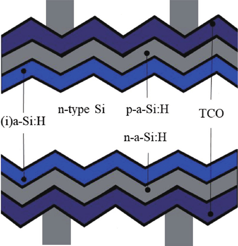
    Fig. 1. (Color online) Structure of the proposed bifacial HIT solar cell.
    (Color online) Density of states diagram of the emitter layer.
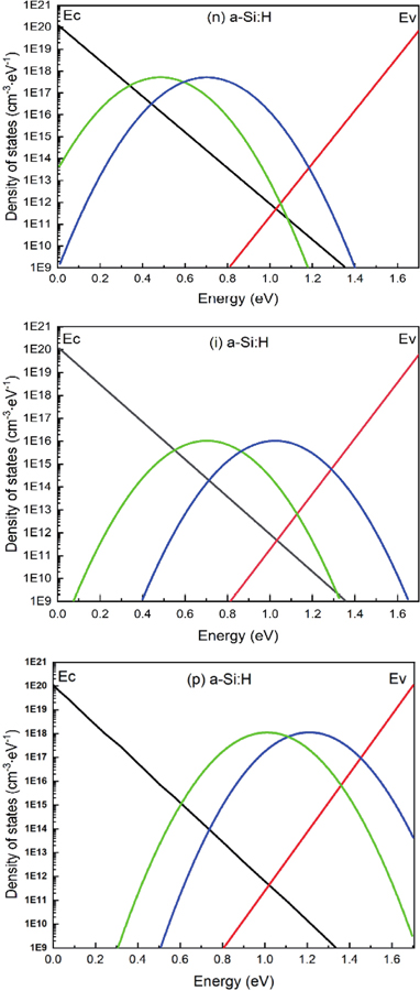
    Fig. 2. (Color online) Density of states diagram of the emitter layer.
    (Color online) Effect of doping concentration.
    Fig. 3. (Color online) Effect of doping concentration.
    (Color online) Effect of gradient doping concentration.
    Fig. 4. (Color online) Effect of gradient doping concentration.
    (Color online) Variation of emitter thickness.
    Fig. 5. (Color online) Variation of emitter thickness.
    (Color online) Effect of electron affinity.
    Fig. 6. (Color online) Effect of electron affinity.
    (Color online) Effect of emitter's band gap energy.
    Fig. 7. (Color online) Effect of emitter's band gap energy.
    (Color online) Effect of hole's mobility.
    Fig. 8. (Color online) Effect of hole's mobility.
    (Color online) Effect of electron's mobility.
    Fig. 9. (Color online) Effect of electron's mobility.
    (Color online) Effect of operation temperature.
    Fig. 10. (Color online) Effect of operation temperature.
    (Color online)J–V curves when the solar cell is illuminated from top side and/or rear side.
    Fig. 11. (Color online)JV curves when the solar cell is illuminated from top side and/or rear side.
    Parameter/layer(n++) nc-Si:Hemitter(i) a-Si:Hbuffer(p++) nc-Si:HBSF(p) c-Siwafer
    Layer thickness (nm)(1–10) × 10–72 × 10–741.8 × 10⁵
    Dielectric constant11.911.911.911.9
    Electron affinity (eV)3.4–4.23.903.954.05
    Band gap (eV )1.4–21.741.3–21.12
    Conduction band density (1020cm3)2.62.62.60.329
    Valence band density (1020cm3)2.62.62.60.3104
    Effective electron (hole) mobility (cm2/(V·s))50 (20)22 (2)50 (20)1009.4 (406.8)
    Doping concentration acceptors (1017cm3)0050000.12
    Doping concentration donators (1020cm3)5000
    Electron (hole) thermal velocity (107cm/s)1 (1 )1 (1)1 (1)1 (1)
    Layer density (g/cm3)2.3292.3292.3292.329
    Auger electron (hole) recombination coefficient (10–31cm6/s)0 (0)0 (0)0 (0)2.9 (0.99)
    Band to band recombination coefficient (10–15cm3/s)0009.5
    Electron (hole) thermal cross section (10–16cm2)7 (7)7 (7)7 (7)
    Total (specific) trap density (1020cm3 )1.36 (20)0.64 (18)16 (20)
    Electron (hole) thermal cross section (10–16cm2)7 (7)7 (7)7 (7)
    Total (specific) trap density (1020cm3 )1.88 (20)0.94 (18.8)2.4 (20)
    Electron (hole) thermal cross section (10–15cm2)3 (30)3 (30)3 (30)
    Total (specific) trap density (1017cm3)690 (1300)0.05 (0.138)689 (1300)
    Energy of distribution (characteristicE) (eV)0.6 (0.21)0.82 (0.144)1.2 (0.21)
    Electron (hole) thermal cross section (10–14cm2)3 (0.3)3 (0.3)3 (0.3)1 (1)
    Total (specific) trap density (1017cm3 )689 (1300 )0.05 (0.138)689 (1300)108 (108)
    Energy of distribution (characteristicE) (eV)0.7 (0.21)0.92 (0.144)1.1 (0.21)0.56
    Table 1. Simulation data used in AFORS.
    Adnan Shariah, Feda Mahasneh. Emitter layer optimization in heterojunction bifacial silicon solar cells[J]. Journal of Semiconductors, 2022, 43(12): 122701
    Download Citation