Abstract
Silicon solar cells continue to dominate the market, due to the abundance of silicon and their acceptable efficiency. The heterojunction with intrinsic thin layer (HIT) structure is now the dominant technology. Increasing the efficiency of these cells could expand the development choices for HIT solar cells. We presented a detailed investigation of the emitter a-Si:H(n) layer of a p-type bifacial HIT solar cell in terms of characteristic parameters which include layer doping concentration, thickness, band gap width, electron affinity, hole mobility, and so on. Solar cell composition: (ZnO/nc-Si:H(n)/a-Si:H(i)/c-Si(p)/a-Si:H(i)/nc-Si:H(p)/ZnO). The results reveal optimal values for the investigated parameters, for which the highest computed efficiency is 26.45% when lighted from the top only and 21.21% when illuminated from the back only.Silicon solar cells continue to dominate the market, due to the abundance of silicon and their acceptable efficiency. The heterojunction with intrinsic thin layer (HIT) structure is now the dominant technology. Increasing the efficiency of these cells could expand the development choices for HIT solar cells. We presented a detailed investigation of the emitter a-Si:H(n) layer of a p-type bifacial HIT solar cell in terms of characteristic parameters which include layer doping concentration, thickness, band gap width, electron affinity, hole mobility, and so on. Solar cell composition: (ZnO/nc-Si:H(n)/a-Si:H(i)/c-Si(p)/a-Si:H(i)/nc-Si:H(p)/ZnO). The results reveal optimal values for the investigated parameters, for which the highest computed efficiency is 26.45% when lighted from the top only and 21.21% when illuminated from the back only.Introduction
Silicon solar cells based on the a-Si:H/c-Si heterojunction are among the most efficient solar cells. In a-Si:H/c-Si heterojunction solar cells, the interface quality, and transport properties are crucial. The vast majority of research towards raising the conversion efficiency of a-Si:H/c-Si heterojunction solar cells has focused on improving interface and transport efficiency. In 1991, Sanyo developed an intrinsic a-Si:H thin layer grown by plasma-enhanced chemical vapor deposition (PECVD)[1] on a p-type a-Si:H/n-type c-Si interface to improve interface quality and transport characteristics . A thin intrinsic a-Si:H layer is used between n-type C-Si and the back surface field (BSF)[2] to reduce the rate of recombination at the rear surface and can achieve a conversion efficiency greater than 20%. Bifacial heterojunction with an intrinsic thin layer (HIT) describes this type of solar cell. By improving interface quality, a bifacial HIT solar cell with a conversion efficiency of over 23% was developed on a substrate of practical size (1004 cm2) at a temperature of less than 200oC[3]. The authors of Ref. [4] employed a modeling approach to optimize the device structure and thickness of silicon heterojunction solar cells with TiO2 as a carrier-selective interface to achieve excellent performance, even with thin Si and to reduce the material cost of Si photovoltaics. Lower parasitic absorption in the transparent conducting oxide layer (TCO) of a thin HIT solar cell with a patterned TCO layer can enhance conversion efficiency at the price of a different front contact design. Local etching is used by Ref. [5] to minimize parasitic absorption in both the TCO and front a-Si:H layers. In Ref. [6], lateral conduction of c-Si absorber substitutes the TCO layer in a SHJ solar cell architecture. A fill factor (FF) of 80.7% was obtained to verify the excellent collection of lateral carriers using only the c-Si bulk. Device structure and thickness of HIT solar cells were optimized through modeling by Ref. [7] to achieve a 27% efficiency. Complete modeling simulations are essential to the development and implementation of bifacial PV systems at scale[8,9] provides a comprehensive evaluation of the current state of c-Si bifacial PV performance characterization and modeling. Their paper presents an overview of the future research necessary to overcome the difficulties connected with the characterization and simulation of c-Si biface PV devices. Ref. [10] investigated the correlations between the carrier transport properties and some fundamental cell parameters of HIT solar cells, including doping concentration, a-Si:H/c-Si interface defect density, layer thickness, and the work functions of the transparent conducting oxide (TCO) and back surface field (BSF) layer, using the AFORS software. They conclude that an understanding of the transport qualities can help to increase the cell's efficiency. Their simulation calculations resulted in an efficiency of 27.07%. Ref. [11] studied the influence of defect states and fixed charges at the a-Si:H/p-Si interface on the performance of HIT solar cells. They observed that defect states on the top side of the a-Si:H/p-c-Si interface had a greater impact on the cell performance than those on the bottom side.
In this study, the effect of emitter layer characteristics on solar cell parameters, such as fill factor, open-circuit voltage, efficiency, and short-circuit current, and how it may contribute to the improvement of a solar cell's overall performance are examined. AFORS-HET software was utilized for calculations, and the structure of the cell was TCO/nc.-Si:H(n)/a-Si:H(i)/c-Si(p)/a-Si:H(i)/nc-Si:H(p)/a-Si:H(i)/nc[12].
Structure and simulation data
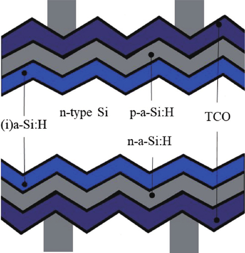
AFORS-HET is used to examine heterojunction c-Si/a-Si:H solar cells. In the calculations, solar radiation with an AM1.5 spectrums and a power density of 100 mW/cm2 is employed, together with flat-band metal contacts and room temperature (300 K). The effective wavelength range was set to the scale (300 to 1200 nm) for which the corresponding absorption coefficient was calculated. TCO, front contact, and back contact are optically simulated with the AFORS-HET program's default material absorption coefficients and refractive indices. Electron/hole pair creation approximated using the Lambert–Beer absorption model for rough surfaces and measured transmission and reflection values.Table 1 displays the input parameters for c-Si/a-Si:H heterojunction solar cells. Standard references inform the distribution of state density across all layers[13-16]. The remaining settings are updated using the values provided by the software[12].Fig. 1 illustrates the proposed HIT solar cell structure. It is predominantly composed of an outer glass cover, a front TCO, and hydrogenated nano-crystalline silicon nc-Si:H (n++ layer) and a-Si:H (intrinsic layer) on top of a crystalline silicon p-layer. On the opposite side of the c-Si layer are deposited a-Si:H (intrinsic layer), nc-Si:H (p++ layer), and a silver grid contact. Due to its high conductivity, low absorption, benign nature, abundant availability, and low processing temperature (200 °C), ZnO was selected as the TCO material. It performs two important functions: anti-reflection on the front surface and frontal protection surface field (FSF) layer to reduce recombination[17].
Table Infomation Is Not Enable

Figure 1.(Color online) Structure of the proposed bifacial HIT solar cell.
Compared to a-Si:H films, hydrogenated nano-crystalline silicon (nc-Si:H) has a wider band gap, lower defect density, and higher conductivity. These characteristics make nc-Si:H(p) an appropriate material for the emitter layer in heterojunction c-Si/a-Si:H solar cells. This emitter layer's high bandgap and fewer defects improve short circuit density and open-circuit voltage, respectively[18].Fig. 2 depicts the density of states diagram for several layers.
Figure 2.(Color online) Density of states diagram of the emitter layer.
Results and discussion
The influence of uniform and gradient emitter doping concentrations
The change of open-circuit voltage (VOC), short-circuit current (JSC), fill factor (FF), and conversion efficiency (η) as a function of doping concentration for a bifacial HIT solar cell is depicted inFig. 3. These parameters are referred to in this text as solar cell parameters (SCP). The emitter layer doping concentration (DOC) varied between 4 × 10¹⁸ and 4 × 1020 cm–3. As doping increases, the cell's efficiency rises to a maximum of 26.4%. This occurred when the DOC was 4 × 1019 cm–3. In fact, as DOC increases, the cell's efficiency decreases until it reaches a value of 25.9% at DOC = 4 × 1020 cm–3. As DOC grows, so does the fill factor, which reaches its maximum value of 85.6% at the same DOC value, 6 × 1019 cm–3, which is the same concentration that maximizes the efficiency. Despite what appears to be the case inFig. 3, variation in DOC has no impact onVOC. In fact, the axis denotingVOC is so abbreviated that the numbers at the beginning and end of its scale is too near together. Despite the fact that this is true, the maximum value ofVOC is 743.5 mV for DOC = 2 × 1019 cm–3. In contrast to what was said previously for the three parameters,JSC has its highest value, 41.6 mA/cm2, while DOC has its lowest value, 4 × 1018 cm–3.JSC drops modestly as DOC increases, and this decline increases after DOC = 2 × 1019 cm–3. This phenomenon can be explained by the fact that the recombination process accelerates as the concentration of doping increases, hence reducing collection of charges.
Figure 3.(Color online) Effect of doping concentration.
AFORS-HET software takes into account various doping mechanisms for each layer of a solar cell, including uniform doping and gradient doping. The aforementioned results were calculated assuming that the emitter has uniform doping. In addition, we perform a second set of calculations assuming a gradient mode for the emitter, with a concentration of 6 × 1019 cm–3 at the top of the layer and a variable concentration at the bottom surface. The computed results are shown inFig. 4. Although SCP values remain unchanged, their dependence on DOC differs in this case. For example, the three,VOC, andJSC have maximal values for low DOC concentrations (corresponds to gradient concentration with a top surface concentration of 6 × 1019 cm–3 and lower surface concentration of 3 × 1016 cm–3. As the concentration increases, the alues of,VOC, andJSC remain steady and begin to fall when DOC reaches 1 × 1019 cm–3. In contrast, the FF begins with a lower value and begins to increase gradually as the DOC on the emitter's bottom surface increases. For gradient doping, it is believed that there is an additional electric field in the emitter layer that has the same direction as the p-n heterojunction's inherent electric field. In addition to the inherent electric field, this electric field has an additional positive effect on the separation of photo-generated carriers, hence enhancing PV performance.
Figure 4.(Color online) Effect of gradient doping concentration.
Optimization of emitter thickness
Fig. 5 depicts the effect of emitter layer thickness variation on SCP. As the emitter's thickness grows, it is apparent that all four SCP drops monotonically. This layer's thickness was increased from 1 to 10 nm. This change diminishes all SCPs, but not in the same manner. Increasing emitter thickness has the greatest impact on efficiency and current density. Since the change in layer thickness accelerates the recombination mechanism, this conclusion is self-evident. The change inVOC is minimal, whereas FF is unaffected. In accordance with the production level and the goal of balancing the output characteristics, it is more practicable to adopt an emitter layer thickness of 1 to 4 nm. As a result, and in light of the simulation findings obtained thus far, the next calculations will take into account a uniform doping mode for the emitter with a concentration of 6 × 1019 cm–3 and a thickness of 4 nm.
Figure 5.(Color online) Variation of emitter thickness.
Variation of emitter's electron affinity
Fig. 6 depicts the influence of the electron affinity on the 4 SCP. As the affinity, χ, increases from 3.7 to 4.1 eV, all SCP parameters increase and tend to stabilize when the affinity is greater than 3.95 eV. The fill factor shows the largest relative increase, increasing from 75%, atχ = 3.7 eV to 85% atχ = 3.95 eV and above.
Figure 6.(Color online) Effect of electron affinity.
Optimization of emitter's band gap energy
The optimization of the nc-Si:H emitter layer band gap energy (Eg)em was performed while maintaining the layer's thickness at 4 nm. The band gap was changed between 1 and 2 eV to accommodate for all conceivable values. The impact of (Eg)em on SCP is depicted inFig. 7. When (Eg)em = 1 eV, the four SCP parameters have reasonable values. Three of these parameters namely;VOC,JSC, and FF increase when the gap energy reaches 1.6 eV, but remain constant when (Eg)em reaches the value of 1.8 eV. The curve of FF shows that this parameter was not affected by the variation of (Eg)em.
Figure 7.(Color online) Effect of emitter's band gap energy.
Effect of hole mobility
The effect of emitter carrier mobility variation on the SCP is depicted in for holes and for electrons. Since the mobility of electrons in silicon is substantially greater than that of holes, the scales utilized in the two figures are different. Consequently, the electron mobility increased from 10 to 250 cm2/(V·s), while the hole mobility increased from 10 to 250 cm2/(V·s). When examining the variation of the hole's mobility, as depicted inFig. 8, the most affected parameters areη andJSC. WhileVOC is only marginally affected, the FF was not affected at all (remains constant). As illustrated inFig. 9, however, the variation in the electron mobility of the emitter (from 10 to 250 cm2/(V·s)) has no effect on the SCP. It is expected since holes are the main carrier in the investigated solar cell.
Figure 8.(Color online) Effect of hole's mobility.
Figure 9.(Color online) Effect of electron's mobility.
Effect of variation of operation temperature
The present work's numerical calculations (simulation) were performed on the assumption that the solar cell operates at a constant temperature of 300 K. However, the impact of a temperature increase varies depending on solar intensity, ambient temperature, wind speed, and so on. Consequently, the temperature of a solar cell may be less than 300 K or larger than 360 K, given that the temperature of a solar cell in hot places during the summer could surpass 80 °C. As seen inFig. 10, we have investigated the influence of cell temperature increase on SCP values in this work. As it can be observed, the rise in cell temperature affects all SCP exceptJSC. In reality, the efficiency of the cell declines from 27.6% to 25.3% when the temperature of the cell rises from 10 to 87 °C. This is primarily due to the decline inVOC. Unlike devices based on crystalline silicon homo-junction technology, silicon heterojunction solar cells (SHJ) have good temperature coefficients (TCs) of 0.23%/°C[3]. This difference in TC between homo-junction and SHJ solar cells at 70 °C might result in relative efficiency losses ranging from 5.4% to 15.8% for a 20% efficient cell.
Figure 10.(Color online) Effect of operation temperature.
The illumination side effect of the bifacial solar cell.
Fig. 11 depicts theJ–V curve when the front and/or back of the solar cell are illuminated. After optimization, the maximum efficiency of the front side illumination is about 26.5%, while the maximum efficiency of the rear side illumination is around 21.5%. This difference is caused by the fact that the light-generated current is proportional to the "collection probability", which specifies the likelihood of a carrier produced by light absorption in a given region of the cell being captured by the p–n junction[19]. However, this probability is dependent on the transit distance of the generated carriers compared to the diffusion length. When the front of the cell receives light, charge carriers are generated, and some of them are collected to form the current. However, when it gets light from the back, the same number of charges will be generated, but the possibility of collecting these charges will be lower. Therefore, the current caused by front illumination is greater than that caused by rear illumination. Consequently, the front face is more effective than the back.
Figure 11.(Color online)J–V curves when the solar cell is illuminated from top side and/or rear side.
Conclusion
This study analyzed the performance of an HIT solar cell with the structure (ZnO/nc-Si:H(n)/a-Si:H(i)/c-Si(p)/a-Si:H(i)/nc-Si:H(p)/ZnO) using the AFORS-HET software. The primary objective was to investigate the properties of the emitter layer (a-Si:H (n++)). The results of the optimization were as follows: (1) The ideal concentration of doping for a nano-crystalline silicon emitter is 6 × 1019 cm–3. (2) This layer's gradient doping is effective and improves the cell's performance. (3) The optimal emitter thickness for improved absorption is 4 nm. (4) Variations in the mobility of holes have a bigger impact on efficiency than variations in the mobility of electrons. (5) The cell's efficiency was 26.46% when lighted from the top only and 21.21% when illuminated from the back only. Therefore, if we can use a concentrator that concentrates the light equally on the front and rear, then we can get a total efficiency of approximately 45%. (6) The temperature coefficient was determined to be approximately –0.23%/°C.
References
[1] Wakisaka K, Taguchi M, Sawada T, et al. More than 16% solar cells with a new ‘HIT’ (doped a-Si/nondoped a-Si/crystalline Si) structure. The Conference Record of the Twenty-Second IEEE Photovoltaic Specialists Conference, 1991, 887
[2] T Sawada, N Terada, S Tsuge et al. High-efficiency a-Si/c-Si heterojunction solar cell. Proceedings of 1994 IEEE 1st World Conference on Photovoltaic Energy Conversion, 2, 1219(1994).
[3] T Mishima, M Taguchi, H Sakata et al. Development status of high-efficiency HIT solar cells. Sol Energy Mater Sol Cells, 95, 18(2011).
[4] D K Gorle, N Chander. A simulation approach for device structure and thickness optimization of silicon heterojunction solar cells featuring TiO 2 as carrier-selective contact. Mater Today Proc, 39, 1916(2021).
[5] R Champory, F Mandorlo, C Seassal et al. Influence of patterning the TCO layer on the series resistance of thin film HIT solar cells. EPJ Photovolt, 8, 80101(2017).
[6] S Li, M Pomaska, A Lambertz et al. Transparent-conductive-oxide-free front contacts for high-efficiency silicon heterojunction solar cells. Joule, 5, 1535(2021).
[7] N Dwivedi, S Kumar, A Bisht et al. Simulation approach for optimization of device structure and thickness of HIT solar cells to achieve ~27% efficiency. Sol Energy, 88, 31(2013).
[8] Libal J, Kopecek R. Bifacial Photovoltaics: Technology, applications and economics. Institution of Engineering and Technology, 2018
[9] T S Liang, M Pravettoni, C Deline et al. A review of crystalline silicon bifacial photovoltaic performance characterisation and simulation. Energy Environ Sci, 12, 116(2019).
[10] J Liu, S H Huang, L He. Simulation of a high-efficiency silicon-based heterojunction solar cell. J Semicond, 36, 044010(2015).
[11] L Oppong-Antwi, S H Huang, Q N Li et al. Influence of defect states and fixed charges located at the a-Si:H/c-Si interface on the performance of HIT solar cells. Sol Energy, 141, 222(2017).
[12] R Varache, C Leendertz, M E Gueunier-Farret et al. Investigation of selective junctions using a newly developed tunnel current model for solar cell applications. Sol Energy Mater Sol Cells, 141, 14(2015).
[13] V Kanneboina. The simulated performance of c-Si/a-Si:H heterojunction solar cells with nc-Si:H, µc-Si:H, a-SiC:H, and a-SiGe:H emitter layers. J Comput Electron, 20, 344(2021).
[14] F Azzemou, D Rached, W Rahal. Optimisation of emitter properties for silicon heterojunction solar cell ITO/pa-Si:H/ia-Si:H/nc-Si/BSF/Al. Optik, 217, 164802(2020).
[15] H B Huang, G Y Tian, L Zhou et al. Simulation and experimental study of a novel bifacial structure of silicon heterojunction solar cell for high efficiency and low cost. Chin Phys B, 27, 038502(2018).
[16] S Kim, H Park, D P Pham et al. Design of front emitter layer for improving efficiency in silicon heterojunction solar cells via numerical calculations. Optik, 235, 166580(2021).
[17] P Sathya, R Natarajan. Design and optimization of amorphous based on highly efficient HIT solar cell. Appl Sol Energy, 54, 77(2018).
[18] Y Yao, X Y Xu, X M Zhang et al. Enhanced efficiency in bifacial HIT solar cells by gradient doping with AFORS-HET simulation. Mater Sci Semicond Process, 77, 16(2018).
[19] Honsberg C, Bowden S. Photovoltaics education website. PV Education, 2019