• Photonics Research
  • Vol. 2, Issue 1, 31 (2014)
A. M. Lerer*, I. V. Donets, G. A. Kalinchenko, and P. V. Makhno
Author Affiliations
  • Physics Department, Southern Federal University Rostov-na-Donu, Zorge St. 5, 344090 Rostov-na-Donu, Russia
  • show less
    DOI: 10.1364/PRJ.2.000031 Cite this Article Set citation alerts
    A. M. Lerer, I. V. Donets, G. A. Kalinchenko, P. V. Makhno. Volume integral method for investigation of plasmonic nanowaveguide structures and photonic crystals[J]. Photonics Research, 2014, 2(1): 31 Copy Citation Text show less
    Structures under consideration.
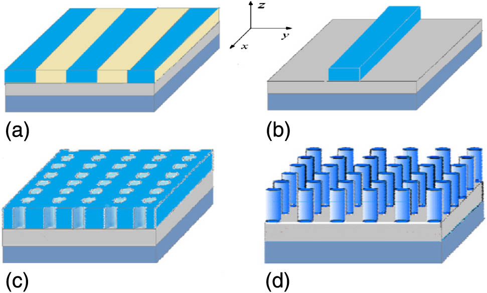
    Fig. 1. Structures under consideration.
    Solid curves represent dispersion characteristics and effective propagation length for the metal waveguide shown in the inset. The red curves correspond to b=20 nm, black to 15 nm. The dashed curves depict analytical solutions for thin-film waveguides.
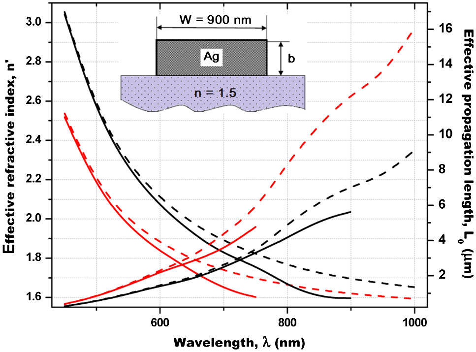
    Fig. 2. Solid curves represent dispersion characteristics and effective propagation length for the metal waveguide shown in the inset. The red curves correspond to b=20nm, black to 15 nm. The dashed curves depict analytical solutions for thin-film waveguides.
    Dispersion characteristics and effective propagation length for the metal waveguide shown in the inset. The red curves correspond to W=500 nm; green, 900 nm; and black, infinity.
    Fig. 3. Dispersion characteristics and effective propagation length for the metal waveguide shown in the inset. The red curves correspond to W=500nm; green, 900 nm; and black, infinity.
    Dispersion characteristics and effective propagation length for the metal waveguide shown in the inset. All dimensions are in nanometers.
    Fig. 4. Dispersion characteristics and effective propagation length for the metal waveguide shown in the inset. All dimensions are in nanometers.
    Dispersion characteristics for the metal waveguide shown in the inset.
    Fig. 5. Dispersion characteristics for the metal waveguide shown in the inset.
    Dispersion characteristics of waves propagating at different angles to the axis x in all-dielectric PC [Fig. 1(c)]. Black solid curves correspond to φ=0°, green to φ=10°, red to φ=12°, and blue to φ=14°. The dashed curves depict the result for φ=0° obtained by Ansoft HFSS commercial software. All dimensions are in nanometers.
    Fig. 6. Dispersion characteristics of waves propagating at different angles to the axis x in all-dielectric PC [Fig. 1(c)]. Black solid curves correspond to φ=0°, green to φ=10°, red to φ=12°, and blue to φ=14°. The dashed curves depict the result for φ=0° obtained by Ansoft HFSS commercial software. All dimensions are in nanometers.
    Normalized losses (top) and dispersion characteristics (bottom) for PC made of perforated silver film placed over a dielectric substrate [Fig. 1(c)]. Waves propagate at the angle φ=0°. Green symbols correspond to zero harmonics, blue to −1st harmonics. Red solid curve corresponds to nonperforated film.
    Fig. 7. Normalized losses (top) and dispersion characteristics (bottom) for PC made of perforated silver film placed over a dielectric substrate [Fig. 1(c)]. Waves propagate at the angle φ=0°. Green symbols correspond to zero harmonics, blue to 1st harmonics. Red solid curve corresponds to nonperforated film.
    Dispersion characteristics for PC made of silver cylinders placed on a two-layer dielectric structure [Fig. 1(d)]. The dielectric layer thickness is b=100 nm on the upper graph and b=150 nm on the lower graph. The red symbols refer to cylinders of 70 nm diameter, black to 90 nm. A wave propagates at the angle φ=0°.
    Fig. 8. Dispersion characteristics for PC made of silver cylinders placed on a two-layer dielectric structure [Fig. 1(d)]. The dielectric layer thickness is b=100nm on the upper graph and b=150nm on the lower graph. The red symbols refer to cylinders of 70 nm diameter, black to 90 nm. A wave propagates at the angle φ=0°.
     Exact SolutionApproximate Solution
    λ, nmReβ/nImβ/ReβReβ/nImβ/Reβ
    4501.365770.053571.364380.04643
    5001.227120.022661.227020.02048
    5501.160680.012511.160660.01156
    6001.122890.008411.122880.00785
    7001.078940.005091.078940.00478
    8001.055870.003041.055870.00289
    Table 1. Complex Refractive Index Obtained with Eqs. (5) and (6) for E-Wave Propagating on the Boundary of Half-Infinite Silver and Dielectric Layers
     Exact SolutionApproximate Solution
    λ, nmReβ/nImβ/ReβReβ/nImβ/Reβ
    5002.620730.054292.620300.04906
    2.113500.025662.113240.02312
    5502.362650.035242.362550.03238
    1.992800.014511.992760.01336
    6002.210510.026262.210460.02429
    1.923960.009891.923940.00919
    7002.023540.017772.023490.01643
    1.843360.006051.843340.00562
    8001.924830.011141.924820.01039
    1.801170.003621.801300.00342
    Table 2. Complex Refractive Index Obtained with Eqs. (5) and (6) for E-Wave Propagating in Vacuum-Silver Film-Dielectric Structure
      Our ResultsData from [28]
    f, THzλ, nmnL0(μm)nL0(μm)
    5006001.293052.9841.283
    4007501.2068314.6901.2117
    30010001.1671123.4381.1723.3
    20015001.1505124.7361.1433.3
    Table 3. Effective Refractive Index and Effective Propagation Length Obtained with Volume Integral Method and Full-Vectorial Finite Difference Method for Linear Oblique and Curved Interfaces for E-Wave Propagating in Rectangular Gold Groove
    A. M. Lerer, I. V. Donets, G. A. Kalinchenko, P. V. Makhno. Volume integral method for investigation of plasmonic nanowaveguide structures and photonic crystals[J]. Photonics Research, 2014, 2(1): 31
    Download Citation