A. M. Lerer, I. V. Donets, G. A. Kalinchenko, P. V. Makhno, "Volume integral method for investigation of plasmonic nanowaveguide structures and photonic crystals," Photonics Res. 2, 31 (2014)
Copy Citation Text
A vector integral–differential equation to describe electromagnetic wave propagation in nanowaveguides and photonic crystals containing thin metal layers is developed. Exact solution of the equation is obtained with the Galerkin method, taking into account the complex dielectric permittivity of metals in the optical range. A simple method for finding complex effective refractive indices for low-loss waveguide structures is developed and proved. Surface plasmon-polariton waves are simulated in the structures under consideration.
1. INTRODUCTION
Implementation of photonic and plasmonic nanostructures significantly expands horizons in signal processing. Very soon the unique capabilities of plasmonic waveguides to manipulate light signals in volumes less than the diffraction limit will allow us to increase device densities in integrated photonic circuits. Plasmonic-based sensors and detectors have already been used in biomedicine and optical communications [1]. Continuing development of plasmonic nanostructures is constantly fueling the exploration of new physical regimes in quantum optics and atomic physics. Progress in the next generation of nanophotonic circuits is defined by new manufacturing technologies [2] and by progress in mathematical methods, allowing better understanding of the physics of the phenomena emerging from interactions of individual photonic, plasmonic, electronic, and mechanical components [3].
In order to use nanowaveguides as connecting wires for information signal transfer, a variety of plasmonic structure designs have been studied recently. These include, for example, metallic strips [4,5], three-layer metal–dielectric structures [6–9], dielectric-loaded surface plasmon-polariton (SPP) waveguides [10,11], and metal grooves [12–14], and -shaped metal wedges [11,15].
Optical media with regularized insertions were studied by Yablonovich in [16]. These media were called photonic crystals (PCs) because of a bandgap presence [17]. Over the past several years, various two-dimensional PCs, composed mostly of cylindrical insertions, have been investigated. A detailed review of these investigations is presented in the book by Bankov [18]. Recently, new simplified technologies were developed for manufacturing three-dimensional PCs made of microcylinders placed between two multilayer films [19].
Sign up for Photonics Research TOC. Get the latest issue of Photonics Research delivered right to you!Sign up now
Compact plasmon waveguides generally suffer from dissipative losses because of high absorption in metals [20,21]. To solve the absorption problem, researchers began to use thin metal nanolayers alternating with dielectric layers, where plasmons can propagate on metal–dielectric borders [22]. This approach gave impressive results—signals propagated on 2.5 cm [23], but the gold waveguide was wide.
Nanophotonic circuit designers are now trying to reach an optimal balance of wave confinement and absorption losses in plasmonic waveguides.
There is a wide range of methods for modeling of electromagnetic wave diffraction and propagation. For a limited number of boundary problems, there are analytical solutions. For example, for diffraction on spheres, there is Mie theory [3].
The majority of numerical methods for calculation of an electromagnetic field in the resonant band can be split in two groups. The first group—the methods based on direct solution of wave equations with defined boundary conditions—includes finite-difference time-domain, the finite element method, and the finite integration technique. In the second group of methods, the boundary problem is reduced to the solution of integrals, the integral–differential, pairs of integrals, and pairs of sum equations.
Without doubt, the advantage of the first group of methods is their versatility. Their disadvantages are high requirements for a computer, long calculation time, the need to digitize not only the scattering object, but also the space around the scatterer, and difficulties with simulations of small-scale elements. In addition, there are problems with satisfaction of boundary conditions for radiation to open space. For the second group of methods these problems are absent. The choice of the integral equation (IE) type, first and foremost, is defined by the structure of the object under investigation. Therefore, the methods based on the IE solution are not as universal as the methods in the first group, but computer programs created based on them work several orders of magnitude faster.
There are several types if IE describing diffraction on dielectric bodies. The majority of them can be split in two groups—surface IE (SIE), where the unknown variable is the field on the dielectric border, and volume IE (VIE), where the unknown variable is the field in all internal points of a body. VIEs have several advantages: they are simpler than surface ones [24, 25], inhomogeneity and nonlinearity do not make simulations more complicated, as happens in the case of surface equations, and the method gives an electrical field inside of a dielectric as the equation solution.
The main goal of this paper is development of a new semi-analytical method to solve the vector integral–differential equation, describing electromagnetic wave propagation in three-dimensional periodic metal–dielectric structures, and a theoretical investigation of PCs and waveguides.
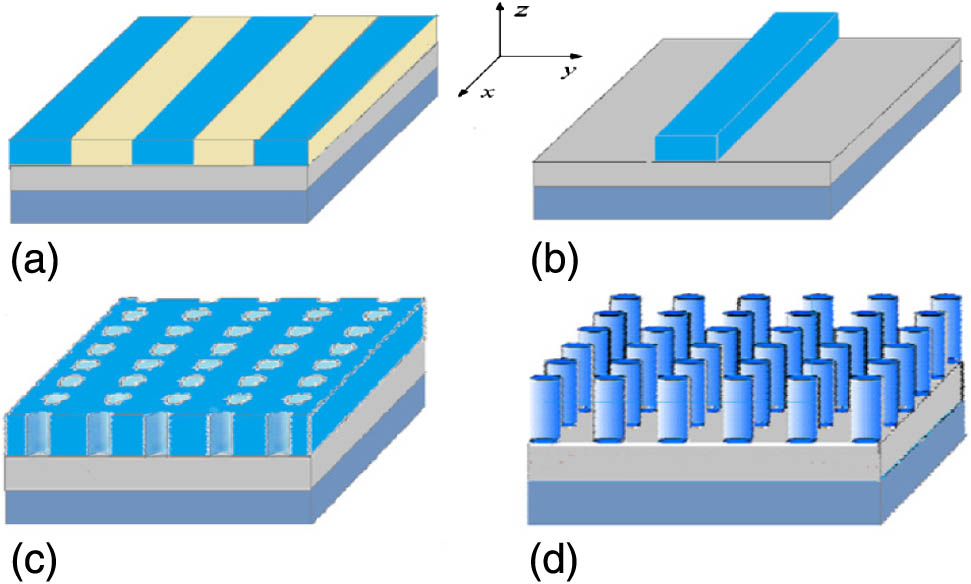
The subject of investigation is planar multilayer dielectric structures with dielectric insertions; see Fig 1. The insertions can be two-dimensional periodic with period , and one-dimensional periodic with periods . Dielectric layers are parallel to the plane, . The number of layers in a structure is arbitrary, the top and bottom layers are half-infinite, the thickness of an internal layer is , and layer numeration is from top to bottom. An electromagnetic wave propagates at angle to axis . The horizontal cross section of the insertion has an elliptical shape, and the ellipse size depends on vertical coordinate ; the vertical cross section is a trapezium. Because the number of insertions and their locations are arbitrary, we can simulate structures of absolutely arbitrary cross section. The dielectric constants of the layers are complex, which makes it possible to consider metal layers in the optical range.
In Lerer’s paper [25] the problem of diffraction on a multilayer two-dimensional dielectric diffraction grating was reduced to the solution of a VIE. Since the structure is periodic, the VIE is solved only inside volume of one insertion: where where is the field at the point of observation, is the wave number in vacuum, is the effective RI (ERI), and and are the dielectric permittivities of an insertion and an ambient layer at the point of observation . The expressions for the elements of tensor Green function are developed in [25]. VIE (1) is bisingular [24], and numerical simulation methods are supposed to take this fact into account. An effective method for simulating optical metallic nanovibrators is presented in papers [24] and [25]. The method is based on integral representation of the Green function, and the VIE was reduced to a set of linear algebraic equations (SLAEs) and solved by the Galerkin method. The VIE kernel singularity shows itself in slow convergence in the matrix elements of the SLAE. It is simpler to improve the convergence than to achieve integral kernel singularity regularization. This approach was used in this work. We seek a solution in the form of where are unknown coefficients, are the basis functions (BFs) are the Bessel functions of the first kind, and are the zeros of the derivative of the Bessel function, i.e., . Coordinates , are expressed via , : , are the ellipse axes in the cross section with coordinate , and is the BF on coordinate . Here we used spline functions of first kind: .
Substitute Eqs. (2) and (3) into Eq. (1), multiply by ; ; ; , and integrate over the volume of an insertion. As a result, we obtain the SLAE relative to unknowns . All integrals in the matrix elements of the SLAE we find analytically. The condition when the SLAE determinant is equal to zero defines the equation for finding the ERI of the structure.
The matrix elements are expressed through a double series on , [see Eq. (1)], and the series summation takes the major part of computing time. We propose a simple method to improve the series convergence. When where is a certain programmed number, we substitute the series of terms by their asymptotes, and neglect the oscillating term of the asymptotes. For the summing up of the remainder of series we used the first term of the Euler–Maclaurin formula, i.e., summation over , is substituted by integration over , . This convergence improvement method lets us reduce the number of series terms and calculation time 16–25 times without a loss in accuracy. For calculations with accuracy as high as 0.1% it is enough to take two–three angular BFs , and the same number of radial BFs . The quantity of BFs is defined by the profile of an insertion, and the ratio of the insertion height to wavelength. To reach the accuracy mentioned above it is enough to take 6–8 functions per one wavelength along the insertion.
Let us consider a one-dimensional grating made of waveguides with periodicity in the direction. In this case, the electric field dependence on coordinate in Eq. (1) can be expressed as , and the series on does not exist. If an electromagnetic wave propagates across the grating (), the VIE [Eq. (1)] splits into two equations, describing propagation of TE and TM waves. For the rest of cases the wave is hybrid. We seek a solution in the form of where are the unknown coefficients, are BFs, and where are Legendre polynomials, is the insertion center coordinate, is the insertion half-width in the cross section, is the knot of the spline function , and we select the constant in the way which lets Fourier transform of in Eq. (1) to be expressed with the formula For a one-dimensional grating the asymptotic series can be summed up analytically.
3. COMPLEX ROOTS RETRIEVAL
The propagation constant is complex in waveguides with complex dielectric constants. Finding complex roots of complex functions is a difficult problem. The main problem is root localization in the complex plane. The roots can be localized by using the principle of the argument. However, its numerical implementation requires multiple calculations of a function, which leads to a long computation time for complex structures. For practical needs, the waves with low losses are the most interesting. In this case, the complex root search process can be simplified in the way described below. Express our propagation constant as . In the low-loss case we have and can use only three terms of the Taylor series expansion: Because is an analytical function, its derivatives do not depend on a direction. The derivatives can be substituted by finite differences: We have Thus, to find a complex propagation constant we need to find three real propagation constants for dielectric waveguides with real dielectric permittivity and use Eq. (5).
We can prove this approach with following tests:
An -wave is propagating on the boundary of half-infinite media. The first medium is a dielectric with refractive coefficient , and the second medium is silver [26]. The analytical solution for this case is well known: where is the wave number in vacuum.
In Table 1 are presented the results for complex RI obtained with Eqs. (5) and (6).
An -wave in the waveguide made of three layers: the first layer is vacuum (half-infinite), the second layer is silver film (thickness 20 nm, upper numbers; 50 nm, lower numbers in Table 2), and the third is half-infinite substrate with RI 1.7. It is known that for this type of waveguide there is an analytical dispersive equation [27]. The equation can be solved numerically. Let us call it an “accurate solution.” The solution obtained with Eq. (5) is called an “approximate solution.” The approximate and accurate solutions are presented in Table 2. Tables 1 and 2 show that the accuracy of approximate solution rises when losses go down. The error of calculation of phase speed does not exceed 1%. The error of loss coefficient calculation is 1 order of magnitude higher.
The third test (Table 3) depicts a comparison of our results to the results from Ref. [28], where the authors used full-vectorial finite difference method for linear oblique and curved interfaces (FVFD-LOCI). We simulated an ERI and effective propagation length for a 120 nm wide and 1200 nm deep rectangular groove made in a gold layer. The effective propagation length in our work is defined the same as in [28]: Data from [28] for Table 3 were taken from graphs and show graphical accuracy.
We simulated the rib waveguide structure from [29], where the authors used the finite element method. Their number for the complex propagation constant is μ; our method gives μ. Thus, the deviation of the complex part is about 10%, which can be explained by the fact that the height and width of the structure in [29] is limited, but we simulated an infinite structure. Also we simulated a metal strip placed between two dielectric layers to compare with the results from [30], where the authors used the commercial code FIMMWAVE. Our numbers for are 0.0002 higher. Because the imaginary part of ERI in [30] is depicted on a logarithmic scale, and an exact comparison is difficult, we can claim about 10% difference between our and their results.
Exact Solution
Approximate Solution
λ, nm
Reβ/n′
Imβ/Reβ
Reβ/n′
Imβ/Reβ
450
1.36577
0.05357
1.36438
0.04643
500
1.22712
0.02266
1.22702
0.02048
550
1.16068
0.01251
1.16066
0.01156
600
1.12289
0.00841
1.12288
0.00785
700
1.07894
0.00509
1.07894
0.00478
800
1.05587
0.00304
1.05587
0.00289
Table 1. Complex Refractive Index Obtained with Eqs. (5) and (6) for E-Wave Propagating on the Boundary of Half-Infinite Silver and Dielectric Layers
Table 3. Effective Refractive Index and Effective Propagation Length Obtained with Volume Integral Method and Full-Vectorial Finite Difference Method for Linear Oblique and Curved Interfaces for E-Wave Propagating in Rectangular Gold Groove
The accuracy of our method can be increased by adding fourth term of the Taylor series expansion in Eq. (5), but it increases the calculation time and does not have practical sense. Errors of experimental measurements for losses are much higher than for phase speed.
4. SIMULATION RESULTS
The C++ numerical code we developed is a clone of the code for the calculation of diffraction of an electromagnetic wave on a diffraction grating [25]. Results obtained with the code are confirmed by multiple theoretical and experimental results of other authors. For example, the results of rectangular dielectric waveguide simulation by the finite element method [31,32], and the results of the VIE solution by modified collocation method for one-dimensional PCs [33,34].
A. Nanowaveguides
As we mentioned above, our code is a modification of the code for simulations of wave diffraction on a diffraction grating [Fig. 1(a)]. Therefore, similar to the eigenwave spectrum of a diffraction grating, two types of waves do exist in a nanowaveguide spectrum. The waves of the first type have their field confined along the waveguides (grating grooves). Their phase velocity and their losses are not sensitive to a change in grating period or on phase shift for the period. The second type of wave, so-called screen waves, are not confined; their phase velocity depends on a grating period and phase shift for the period. Screen waves are not interesting to us. Here, we consider a nanowaveguide [see Fig. 1(b)] as part of a diffraction grating [see Fig. 1(a)] with infinite period.
Figures 2 and 3 present the results of simulations of a simple rectangular silver waveguide [see Fig. 1(b)], placed on a silica dielectric substrate. It is well known that a surface wave (plasmon-polariton) propagates at the metal–dielectric boundary, and the wave speed depends on the dielectric RI. This means that, in a waveguide composed of a metal film placed between the two dielectrics, there are two waves on each surface of the metal film.
Figure 2.Solid curves represent dispersion characteristics and effective propagation length for the metal waveguide shown in the inset. The red curves correspond to , black to 15 nm. The dashed curves depict analytical solutions for thin-film waveguides.
Figure 3.Dispersion characteristics and effective propagation length for the metal waveguide shown in the inset. The red curves correspond to ; green, 900 nm; and black, infinity.
When film is thick, these waves do not interact; they correspond to the waves for two well-known independent structures: air–metal and metal–substrate. When the film thickness is reduced the waves begin to interact, which leads to effective refraction index growth, and to the increase of losses. In Fig. 2, losses are presented through effective propagation length. Comparing a rectangular waveguide and the same thickness thin film waveguide, we can see that losses and ERI of the rectangular one are higher because of field appearance on the rectangle’s sides. For a short wavelength, the field is mostly confined at the metal–substrate boundary and the characteristics of the waveguide almost do not depend on its width. Side field impact increases and decreases when wavelength or waveguide thickness goes up, and when the waveguide width goes down. Waveguides with limited width have a long wave cutoff at less than substrate RI because the wave leaks into the substrate. The critical wave length decreases with increased thickness of the waveguide and reduction of its width.
In Fig. 4 we present simulation results of a simple dielectric nanowaveguide [see Fig. 1(b)]; a dielectric strip of a rectangular cross-sectional shape is placed over silver film deposited on a dielectric substrate. Figure 4 shows the wavelength range where SPPs can propagate. In this range the ERI is higher than the RI of the dielectric strip . The ERI, presented in Fig. 4, increases when the width and height of the strip increases and decreases when thickness of the metal film decreases. In Figs. 2–4, we can see that the propagation length for waveguides made of a dielectric strip on a metal film and for a metal strip on a dielectric layer are approximately the same.
Figure 4.Dispersion characteristics and effective propagation length for the metal waveguide shown in the inset. All dimensions are in nanometers.
Figure 5 shows the characteristics of a dielectric waveguide with a trapezoidal cross-sectional shape. , of course, grows with and increase in , but dependence () is weak. This means that the concentration of the electromagnetic field near the border of the dielectric strip and metal film is high.
Figure 5.Dispersion characteristics for the metal waveguide shown in the inset.
In this work we investigated three types of photonic crystals (PC). The first one is sieve-looking, made of several dielectric layers with round periodic holes in them. In particular, the structure consists of three layers of dielectric placed on a dielectric substrate, as shown in Fig. 6. The two-dimensional grating is perforated in two upper layers. As can be seen from Fig. 6, the PC has a window of opacity. In the opacity window area the phase velocity of the zero harmonic with a normal dispersion (; , are the numbers of spatial harmonics on the and axes, respectively) and the st harmonic with anomalous dispersion (, ) become equal, and dispersion curves for both harmonics merge and make one wedge-looking curve. From the equality of phase speeds for these spatial harmonics, it follows that the wavelength in the middle of the opacity window satisfies the condition where is the PC period. At this wavelength, the waves reflected from neighboring insertions interfere in phase, and wave propagation in the PC becomes impossible. In Fig. 6 we can see that the opacity window moves toward shorter wavelengths when the angle of propagation changes from 0° to 14°, which is consistent with Eq. (7).
Figure 6.Dispersion characteristics of waves propagating at different angles to the axis in all-dielectric PC [Fig. 1(c)]. Black solid curves correspond to , green to , red to , and blue to . The dashed curves depict the result for obtained by Ansoft HFSS commercial software. All dimensions are in nanometers.
Also, from our calculations, we found that a wave with wavelength longer than 665 nm cannot propagate in the structure in Fig. 6 if we remove reflecting heterogeneities in the form of air holes. This happens because the ERI of such a layered structure without holes becomes smaller than the substrate RI, and the wave leaks into the substrate. For comparison of the VIE method with modern numerical methods, we simulated this structure by HFSS code, and show the result in Fig. 6 as a dashed curve.
In Fig. 7, a plasmon wave propagates on the boundary of a perforated silver layer and a dielectric substrate. Losses at the edges of the opacity window drastically increase, and in the framework of a low-loss model, we cannot close the curves. For , ERI is less than the substrate RI and the wave leaks into the substrate.
Figure 7.Normalized losses (top) and dispersion characteristics (bottom) for PC made of perforated silver film placed over a dielectric substrate [Fig. 1(c)]. Waves propagate at the angle . Green symbols correspond to zero harmonics, blue to st harmonics. Red solid curve corresponds to nonperforated film.
Figure 8 shows the dispersion curves for a structure made of one dielectric layer with a two-dimensional periodic system of silver cylinders deposited on a semi-infinite dielectric substrate. As can be seen from the figure, the increase of cylinder diameters leads to higher losses and a wider opacity window. The short-wave edge of the window almost does not change with a change of cylinder diameter. The PC at the top of Fig. 8 works as a high-frequency filter.
Figure 8.Dispersion characteristics for PC made of silver cylinders placed on a two-layer dielectric structure [Fig. 1(d)]. The dielectric layer thickness is on the upper graph and on the lower graph. The red symbols refer to cylinders of 70 nm diameter, black to 90 nm. A wave propagates at the angle .
The Galerkin method is implemented to find the exact solution of a vector integral–differential equation to describe electromagnetic wave diffraction on three-dimensional bodies with complex dielectric permeability. The solution obtained is applied to the investigation of electromagnetic wave propagation in one- and two-dimensional plasmonic structures. A new simple method for finding the complex refractive index for low-loss structures is proposed and proved. Three types of nanowaveguide and three types of PC were simulated. A possibility of propagation of surface plasmonic waves with high effective refractive index is predicted.
[31] V. A. Kuznetsov, A. M. Lerer. Dispersion characteristics of rectangular dielectric waveguide. Radio Eng. Electron. Phys., 27, 24-27(1982).
[32] V. A. Kuznetsov, A. M. Lerer. Dispersion characteristics of dielectric waveguides on substrates. Radio Eng. Electron. Phys., 29, 53-58(1984).
[33] G. A. Kalinchenko, A. M. Lerer. Investigations of dielectric gratings using electrodynamic models based on volume integral equations. J. Commun. Technol. Electron., 48, 1221-1227(2003).
A. M. Lerer, I. V. Donets, G. A. Kalinchenko, P. V. Makhno, "Volume integral method for investigation of plasmonic nanowaveguide structures and photonic crystals," Photonics Res. 2, 31 (2014)