
Bowen Liu, Jiangtao Xu. Modeling the photon counting and photoelectron counting characteristics of quanta image sensors[J]. Journal of Semiconductors, 2021, 42(6): 062301
- Journal of Semiconductors
- Vol. 42, Issue 6, 062301 (2021)
Abstract
1. Introduction
The quanta image sensor (QIS)[
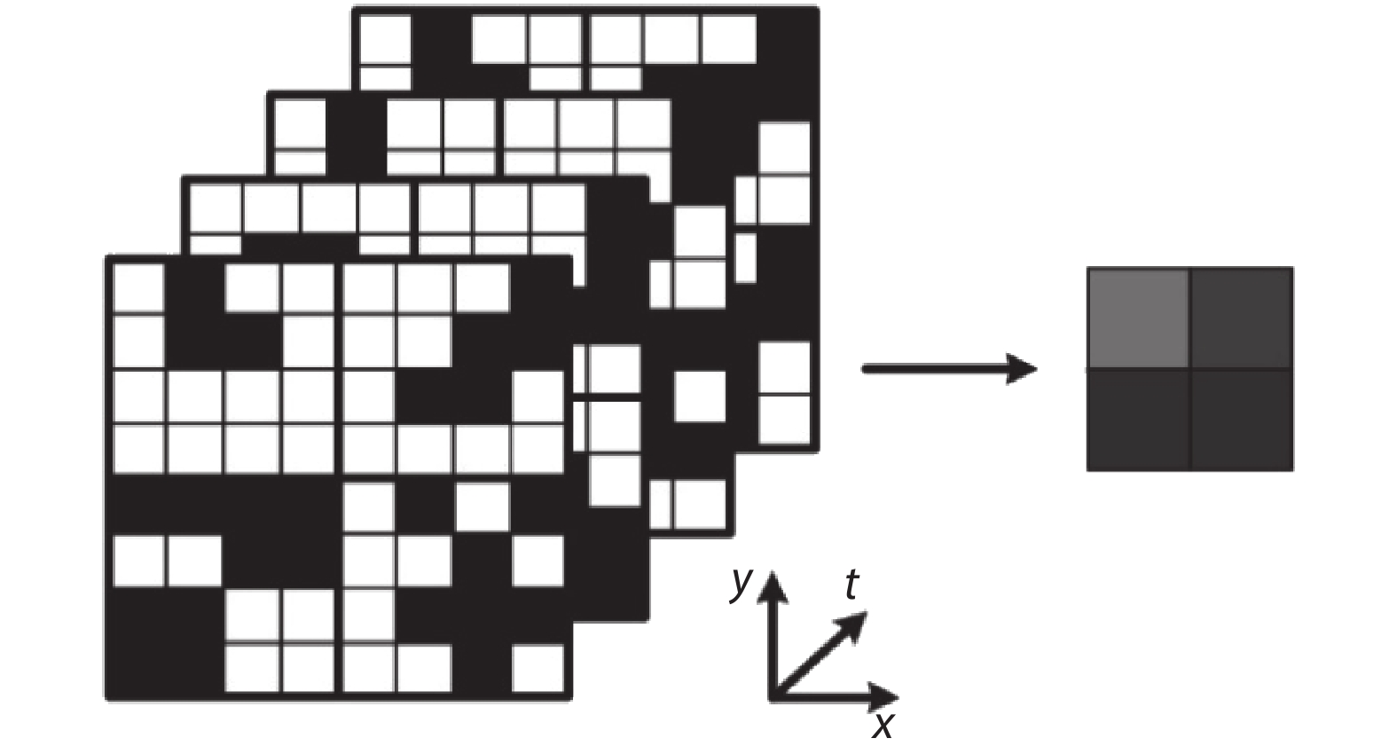
To intuitively comprehend the concept of the QIS, a conceptual illustration is shown in Fig. 1. As shown in Fig. 1, the output of the QIS is a large spatial-temporal data cube that can be flexibly combined in subsequent image processing.
![]()
Figure 1.The QIS conceptual illustration. An 8 × 8 × 4 spatial-temporal data cube of jots in the QIS (left) is reconstructed to a 2 × 2 data plane of pixels in the output image (right). Each data of pixels is equal to the sum of a 4 × 4 × 4 data sub-cube of jots.
The main development direction of image sensors is high integration, high performance, and low cost. Therefore, the size of active pixels in CISs keeps shrinking to achieve higher resolution on a smaller chip size, which meets the needs of high integration and low cost. Nevertheless, the shrinkage of pixels causes the problem of full well capacity (FWC) decrease that leads to signal-to-noise ratio (SNR) and dynamic range (DR) decreases[
To alleviate the problem of FWC decrease, the QIS, which is a candidate for the next-generation solid image sensor, was first introduced in 2005[
The prospective application fields of QISs include consumer imaging, low-light imaging, security monitoring imaging, scientific imaging, medical imaging, and space imaging. When the image performance strongly depends on the absolute measurements of incident photons, especially in scientific and medical imaging, high accuracy photon and photoelectron counting is required. Therefore, the high accuracy photon and photoelectron counting characteristics of QISs should be studied further.
The photoresponse characteristic of QISs, which is referred as D–logH response, was theoretically derived in Ref. [9] and experimentally proven in Ref. [17]. On the one hand, for high dynamic range (HDR) applications, the overexposure latitude range of the D–logH response curve can be used to extend the DR of the QIS. On the other hand, for applications that need high accuracy photon and photoelectron counting, the non-linear response of overexposure latitude range will increase the counting error of the QIS in high light level, and the non-ideal characteristics, such as dark current and read noise, will increase the counting error of the QIS[
Therefore, the photoresponse and counting error characteristics of QISs, and the effects of non-linear response and non-ideal characteristics to them are needed to be investigated. The high accuracy photon and photoelectron counting exposure ranges of QISs are required to be determined theoretically for subsequent on-chip or off-chip calibrations, and the integration time optimization under different light level and jot size is one of the common methods.
In this paper, an integration time optimization method towards high accuracy photon and photoelectron counting is presented to guide the design and operation of single-bit and multi-bit QISs. The remainder of this paper is organized as follows. A signal chain model of single-bit and multi-bit QISs is established in Section 2. The photoresponse characteristics for ideal and realistic QISs are investigated in Section 3. The signal error rates towards photon and photoelectron counting are investigated in Section 4. An optimization method of integration time that can guide the design and operation of QISs is presented in Section 5. Finally, the conclusions are given in Section 6.
2. Signal chain model
2.1. Basic concepts
The signal chain model of single-bit and multi-bit QISs is illustrated in Fig. 2, which contains signal conversion processes of photons to electrons, electrons to voltages, and voltages to digital numbers. The parameters of the signal chain model in Fig. 2 are listed in Table 1.
![]()
Figure 2.The signal chain model of quanta image sensors.
Table Infomation Is Not EnableAs shown in Fig. 2 and Table 1, the input and output signals of the proposed model are kph and DN, respectively. In the jot, kph incident photons arrive at the pinned photodiode and generate kphe photoelectrons on the condition that the quantum efficiency of the jot is QE. Then, kphe photoelectrons and kd dark signal electrons, which are generated from dark current, constitute together ke total signal electrons. Then, ke total signal electrons are transferred to the floating diffusion and converted to VCG on the condition that the conversion gain of the jot is CG. In the readout circuit, VCG is converted to VRO on the condition that the read noise of the readout circuit is vn. In the ADC, VRO is converted to DN on the condition that the quantizer threshold of the ADC is vth.
It is noted that the electron-referred values (i.e., the normalized values) of VCG, VRO, vn, and vth are UCG, URO, un, and uth, respectively. In most cases, the normalized values are introduced because it is more convenient to use them in mathematical derivation. The unit of ro (i.e., ADU) is equivalent to p or e-, when the ADC output digital numbers are compared with photons or photoelectrons. To analyze the proposed signal chain model mathematically, a series of probability distributions are introduced in the following sections.
2.2. Total signal electrons
In the proposed signal chain model, the total signal electrons consist of photoelectrons and dark signal electrons, which are generated from incident photons and dark current in the jot, respectively. As described in Refs. [13, 18], benefiting from the jot device structure and the QIS operating characteristic, the image lag and crosstalk of pump-gate jots in the QIS are acceptable for photon counting and photoelectron counting applications under different exposure levels. Therefore, other sources of total signal electrons, including image lag, optical crosstalk, and electronic crosstalk, are not considered in the proposed model.
The emission of photons from most light sources is well-described by Poisson distribution[
where μph is the mean value of incident photons, and kph is a nonnegative integer.
The quantum efficiency of the jot QE is defined as the number of photoelectrons divided by the number of incident photons. The process that photons convert to photoelectrons obeys binomial distribution[
where kphe and kph are nonnegative integers, and kphe is less than or equal to kph.
Then, the PMF that kphe photoelectrons are generated in the jot under μph and QE, which is the convolution of two mutually independent PMFs Eqs. (1) and (2), is derived as:
where
Similarly, the emission of dark signal electrons that generate from dark current in active pixels also obeys Poisson distribution. Thus, over the integration time τ, the PMF that kd dark signal electrons are generated in the jot is defined as:
where μd is the mean value of dark signal electrons, and kd is a nonnegative integer.
Then, the PMF that ke total signal electrons are generated in the jot, which is the convolution of two mutually independent PMFs Eqs. (7) and (8), is derived as:
where
2.3. Normalized jot output
The total signal electrons are transferred from pinned photodiode (PPD) to floating diffusion (FD) and converted to VCG in the jot, when the conversion gain of the jot is CG that is calculated as:
where q is the electron charge, CFD is the total capacitance of FD, and the unit of CG is usually μV/e-.
Then, the voltage-referred jot output is defined as:
It is convenient to use normalized values to simplify the analysis of the proposed model. Thus, the normalized value (i.e., the electron-referred value) of VCG is calculated as[
In the subsequent derivation, a similar method is used to convert the voltage-referred values VRO, vn, and vth to the normalized values URO, un, and uth, respectively.
2.4. Normalized readout circuit output
The readout circuit in the proposed model contains the source follower (SF), the amplifying circuit, and the correlation double sampling (CDS) circuit before the ADC. The voltage-referred read noise of the readout circuit vn, which contains thermal noise and 1/f noise, is normalized as[
It is noted that only temporal noise is considered in the proposed model. In other words, the spatial noise (i.e., fixed pattern noise (FPN), including dark signal nonuniformity (DSNU) and photoresponse nonuniformity (PRNU)), which may cause by QE, CG, un, and uth nonuniformities among jots array, are not considered in the proposed model.
The main approach of the QIS to achieve photon counting and photoelectron counting is to increase the conversion gain of jots to reduce the electron-referred read noise lower than 0.5 e- r.m.s. (i.e., deep sup-electron read noise level). For example, when vn is equal to 100 μV r.m.s., CG is required to be higher than 200 μV/e-, i.e., CFD is required to be lower than 0.8 fF, to make sure un is lower than 0.5 e- r.m.s..
When the read noise un obeys Gaussian distribution, the component probability density function (PDF) that the normalized readout circuit output URO generates from the normalized jot output UCG is defined as[
Using Eqs. (12), (14), (15), and (17), the PDF that the normalized readout circuit output URO is generated, when the mean value of total signal electrons is μe, is derived as:
where URO is a real number.
The PDF P[URO] as a function of URO on the condition that μe = 2 e- and un = 0.2 e- r.m.s. is shown in Fig. 3 as an example.
![]()
Figure 3.(Color online) The PDF
2.5. ADC output
In the process of quantization, the normalized readout circuit output URO is converted to the ADC output DN based on different quantization levels. For an n-bit QIS, there are 2n quantization levels and 2n – 1 quantization boundaries. The effective full well capacity of the QIS is generally limited by the bit depth of ADC and equal to 2n– 1.
As shown in Fig. 3, for a 2-bit QIS, four quantization levels are N0, N1, N2, and N3, which correspond to 0, 1, 2, and 3 ADU, respectively. When the normalized quantizer threshold uth = 0.5 e-, three normalized quantization boundaries are 0.5, 1.5, and 2.5 e-. When URO∈(–∞, 0.5 e-], DN = 0 ADU; when URO∈(0.5 e-, 1.5 e-], DN = 1 ADU; when URO∈(1.5 e-, 2.5 e-], DN = 2 ADU; when URO∈(2.5 e-, +∞], DN = 3 ADU.
Thus, for an n-bit QIS, the PMF that the ADC output digital numbers DN is generated, when the normalized quantizer threshold is uth, is defined as:
where the higher quantization boundary Uth1 = DN + uth, the lower quantization boundary Uth2 = DN – (1 – uth), the effective full well capacity FWCeff = 2n– 1, and DN is a nonnegative integer.
3. Photoresponse characteristic
Conventional CISs generally have linear response, and some CISs can achieve logarithmic and linear-logarithmic response through pixel or circuit structure design. In contrast from these CISs, the QIS has a special photoresponse characteristic, which is referred to as D–logH response. For high dynamic range applications, the overexposure latitude range of the D–logH response curve is used to extend the dynamic range of the QIS[
3.1. Ideal D–logH photoresponse curves
As shown in Fig. 1, by reconstructing a specified spatial-temporal data cube of jots into a single data point of a pixel in the output image, the trade-off between the equivalent full well capacity, spatial resolution, and temporal resolution can be flexibly achieved. The spatial and temporal oversampling coefficients of the QIS are defined as MS and MT, respectively, and the total oversampling coefficient of the QIS is calculated as:
where M has various spatial-temporal combinations. For example, when M = 512, a 4 × 4 × 32, 8 × 8 × 8, 16 × 16 × 2, et al. sub-cube of jots is alternative.
Assuming the jots used for reconstruction are completely equivalent (i.e., no DSNU and PRNU among jots array), the signal value of ADC output is calculated as:
where
Similarly, the saturated signal value of ADC output is calculated as:
where FWCequ and FWCeff is the equivalent and effective full well capacity respectively, and n is the bit depth of QISs (i.e., the bit depth of ADCs in those QISs). For example, for a 3-bit QIS, when MS = 4 × 4, MT = 8 and M = 4 × 4 × 8 = 128, FWCequ = M · FWCeff = 896 e-.
In Ref. [9], in the D-logH function, H denotes quanta exposure, which is defined as the average number of photons or photoelectrons arrive at a jot over the integration period; and D denotes bit density, which is defined as the number of saturated jots divided by the number of total jots for 1-bit QISs.
In this paper, the D–logH function is extended to n-bit QISs. H denotes quanta exposure, which is defined as the mean value of photons that arrive at a jot over the integration time τ. Thus, H is equal to μph. When QE = 1 e-/p, H is also equal to μphe × 1 p/e-. Meanwhile, D denotes signal density, which is defined as:
where SDN and SDN,sat are given by Eqs. (21) and (22) respectively.
The ideal D-logH response curves for 1-bit, 2-bit, 3-bit, 4-bit, and 5-bit QISs are shown in solid lines in Fig. 4, where QE = 1 e-/p, μd = 0 e-, un = 0 e- r.m.s., and uth = 0.5 e-. The ideal linear response curves for 1-bit to 5-bit CISs are shown in dashed lines in Fig. 4, where the output signal is equal to the input signal (i.e., the ideal accuracy photon counting is achieved).
![]()
Figure 4.(Color online) The ideal
As shown in Fig. 4, when D = 0.99, the saturated quanta exposure Hsat of 1-bit to 5-bit QISs are equal to 4.7, 7.3, 13, 22, and 39 p, respectively. Meanwhile, Hsat of 1-bit to 5-bit CISs are equal to 0.99, 2.97, 6.93, 14.85, and 30.69 p, respectively. Thus, compared with the n-bit CIS, the n-bit QIS has a higher Hsat and a greater potential in HDR applications in theory.
As H increases from 0.01 to 100 p, the QIS gradually enters in the nonlinear response range (the non-overlap range of solid line and dashed line) from the linear response range (the overlap range of solid line and dashed line). As n increases from 1 to 5, the linear and nonlinear response ranges of 1-bit to 5-bit QISs are extended and narrowed respectively. Thus, QISs with higher bit depth are inferred to have a better performance in applications that need high accuracy photon counting and photoelectron counting in theory.
3.2. Realistic photoresponse curves
For realistic QISs, QE < 1 e-/p, μd> 0 e-,un > 0 e- r.m.s., and uth = 0.5 e-. In the realistic response curve for an n-bit QIS, H is equal to μph, and D is calculated as Eq. (23). The realistic response curves for the 3-bit QIS under five different conditions, which are listed in Table 2, are shown in Fig. 5.
![]()
Figure 5.(Color online) The realistic response curves for the 3-bit QIS. The different conditions of curve 1 to 5 are listed in
Based on Fig. 5, the effects of QE, μd, and un to realistic response curves for the QIS are qualitatively analyzed, as follows:
(1) Curve 1 (ideal) is the ideal response curve for the 3-bit QIS as a comparison;
(2) Curve 2 (QE = 0.8 e-/p) can be approximatively considered to be obtained by shifting curve 1 to the right. This means that when QE < 1 e-/p, a higher H is required to get the same D in curve 1;
(3) In curve 3 (μd = 0.01 e-), as H increases from 0.01 p to 100 p, curve 3 gradually coincides with curve 1, the difference of D between curve 3 and curve 1 gradually decreases, i.e., μd > 0 e- has an obvious effect on low light level ( H < 0.1 p);
(4) In curve 4 (un = 0.3 e- r.m.s.), un > 0 e- r.m.s. has a similar effect on low light level ( H < 0.1 p) compared with μd > 0 e- in curve 3;
(5) Curve 5 (QE = 0.8 e-/p, μd = 0.01 e-, and un = 0.3 e- r.m.s.) combines the effects of QE < 1 e-/p, μd > 0 e-, and un > 0 e- r.m.s.. When H is lower than 0.25 p, D in curve 5 is higher than curve 1, μd > 0 e- and un > 0 e- r.m.s. are dominant. When H is higher than 0.25 p, D in curve 5 is lower than curve 1, QE < 1 e-/p is dominant.
In summary, the lower boundary of the linear response range of the QIS is limited by μd and un, the higher boundary of the above range is limited by the bit depth of QISs n, and this range shifts to the right when QE < 1 e-/p. To further study the high accuracy linear ranges towards photon counting and photoelectron counting of ideal and realistic response curves, and the effects of QE, μd, and un to the above ranges of realistic response curves, a quantitative analysis is performed in Section 4.
4. Signal error rate
In this paper, the signal error rate is defined as the absolute value of the difference between the input and output signals divided by the input signal, which is used as the qualifying factor to evaluate the accuracy of photon counting or photoelectron counting for the QIS.
4.1. Signal error rate for ideal QISs
Assuming that the jots used for reconstruction are completely equivalent, like Eq. (21), the signal value of incident photons is calculated as:
Similarly, the signal value of photoelectrons is calculated as:
And the signal error rate between SDN and Sph is defined as:
where SERph is the qualifying factor of evaluating the accuracy of photon counting in the QIS. When SERph is decreased, the difference between SDN and Sph is decreased, and the accuracy of photon counting is increased.
The signal error rate between SDN and Sphe is defined as:
where SERphe is the qualifying factor of evaluating the accuracy of photoelectron counting in the QIS. When SERphe is decreased, the difference between SDN and Sphe is decreased, and the accuracy of photoelectron counting is increased.
In this paper, based on Eqs. (26) and (27), the μph value interval corresponding to SERph < 0.01 is defined as the high accuracy photon counting exposure range (hereinafter to be referred as Rph) or high accuracy linear range of response curves, and the μphe value interval corresponding to SERphe < 0.01 is defined as the high accuracy photoelectron counting exposure range (hereinafter to be referred as Rphe).
As for n-bit ideal QISs, QE = 1 e-/p, μd = 0 e-, un = 0 e- r.m.s., and uth = 0.5 e-. In this case, μphe = μph × 1 e-/p, and SERphe = SERph, i.e., photon counting is equivalent to photoelectron counting when QE = 1 e-/p. And SERph as a function of μph for ideal 1-bit to 5-bit QISs is shown in Fig. 6.
![]()
Figure 6.(Color online) The photon counting signal error rate SERph as a function of the mean value of incident photons
As shown in Fig. 6, for a given n, when μph is increased, SERph is increased; for a given μph, when n is increased, SERph is decreased; for ideal 1-bit to 5-bit QISs, Rph is (–∞, 0.021 p), (–∞, 0.72 p), (–∞, 3.4 p), (–∞, 10 p), and (–∞, 25 p), respectively; in other words, as n increases from 1 to 5, Rph is extended from (–∞, 0.021 p) to (–∞, 25 p).
Based on these results, it can be proven theoretically that increasing the bit depth of the QIS is an effective approach to improve the performance of QISs in applications that need high accuracy photon counting and photoelectron counting.
4.2. Photon counting signal error rate for realistic QISs
As for n-bit realistic QISs, QE < 1 e-/p, μd > 0 e-, un > 0 e- r.m.s., and uth = 0.5 e-. In this case, photon counting is inequivalent to photoelectron counting. To determine the Rph of realistic QISs, SERph as a function of μph for the 3-bit QIS under five different conditions, which are listed in Table 2, is shown in Fig. 7.
![]()
Figure 7.(Color online) The photon counting signal error rate SERph as a function of the mean value of incident photons
Based on Fig. 7, the Rph of curve 1 to 5 is (–∞, 3.4 p), N/A, (0.99 p, 3.6 p), (1.2 p, 3.4 p), and (0.23p, 0.26p), respectively. And the effects of QE, μd, and un to the Rph of the realistic QIS are quantitative analyzed as follows:
(1) Curve 1 (ideal) is the ideal SERph curve for the 3-bit QIS as a comparison;
(2) In curve 2 (QE = 0.8 e-/p), when μph ≤ 1.6 p, SERph remains constant at 0.2; when μph > 1.6 p, SER ph is gradually increased to 1. This means that QE has significant effect on SERph, and QE is the main limit factor of high accuracy photon counting for the QIS;
(3) In curve 3 (μd = 0.01 e-), as μph increases from 0.01 p to 100 p, SERph first decreases from a high value to the minimum value and then gradually increases to 1. The minimum value point (i.e., the optimal point for photon counting) is (μph = 2.7 p, SERph = 2.23 × 10⁻⁴). Compared with curve 1, μd > 0 e- mainly increases the SER ph on low light level (H < 0.1 p);
(4) In curve 4 (un = 0.3 e- r.m.s.), un > 0 e- r.m.s. has a similar effect on SER ph compared with μd> 0 e- in curve 3. The minimum value point of curve 4 is (μph = 2.4 p, SERph = 2.14 × 10⁻⁴);
(5) In curve 5 (QE = 0.8, μd = 0.01 e-, and un = 0.3 e- r.m.s.), the effects of QE < 1 e-/p, μd > 0 e-, and un > 0 e- r.m.s. are combined. As μph increases from 0.01 p to 100 p, SERph first decreases and then increases. The minimum value point of curve 5 is (μph = 0.24 p, SERph = 4.37 × 10⁻³). When μph < 0.13 p, SER ph > 0.2, the effects of μd = 0.01 e- and un = 0.3 e- r.m.s. are dominant; when 0.13 p ≤ μph ≤ 3.5 p, 4.37 × 10⁻³ ≤ SERph ≤ 0.2, the effect of QE = 0.8 e-/p is dominant; when μph > 3.5 p, SER ph is gradually increased to 1 due to the saturation of jots.
The cause of optimal point in curve 5 can be explained through the following example: assuming that 10 photons arrive at the jot and convert to 9 photoelectrons under QE; if 1 dark signal electron is generated, then the number of total signal electrons is 10; thus, a dark signal electron may fill the electron loss due to QE and cause SERph decrease in some special cases.
In summary, when QE is low, Rph is limited by QE; when QE is high enough, such as 0.95 e-/p[
4.3. Photoelectron counting signal error rate for realistic QISs
To determine the Rphe of realistic QISs, SERphe as a function of μph for the 3-bit QIS under five different conditions, which are listed in Table 2, is shown in Fig. 8.
![]()
Figure 8.(Color online) The photoelectron counting signal error rate SERphe as a function of the mean value of incident photons
As shown in Fig. 8, the Rphe of curve 1 to 5 is (–∞, 3.4 p), (–∞, 4.3 p), (0.99 p, 3.6 p), (1.2 p, 3.4 p), and (2.1 p, 4.5 p), respectively. It is noted that since QE = 1 e-/p and SERphe = SERph, curve 1, 3, and 4 in Fig. 8 are the same as Fig. 7.
Curve 2 (QE = 0.8 e-/p) can be approximatively considered to be obtained by shifting curve 1 (ideal) to the right (i.e., Rphe shifts to the right when QE < 1 e-/p).
In curve 5 (QE = 0.8 e-/p, μd = 0.01 e-, and un = 0.3 e- r.m.s.), the effects of QE < 1 e-/p, μd > 0 e-, and un> 0 e- r.m.s. are combined. Asμph increases from 0.01 to 100 p, SERphe first decreases and then increases. The minimum value point of curve 5 is (μph = 3.5 p, SERphe = 1.45 × 10⁻⁴). When μph < 3.5 p, SER phe > 1.45 × 10 –4, the effects of μd = 0.01 e- and un = 0.3 e- r.m.s. are dominant; when μph ≥ 3.5 p, curve 5 gradually overlaps with curve 2, and SERphe is finally increased to 1 due to the saturation of jots.
In summary, the lower boundary of Rphe is limited by μd and un, the higher boundary of Rphe is limited by the bit depth of QISs, and Rphe shifts to the right when QE < 1 e-/p. Therefore, the main approach of extending the Rphe of realistic QISs is increasing n, and decreasing μd and un.
5. Integration time optimization
5.1. Physical explanation
As discussed in Section 4, by calculating SERph and SERphe, the μph and μphe value interval corresponding to SERph < 0.01 and SER phe < 0.01 (i.e., Rph and Rphe) are determined.
In imaging applications, under the specified illuminance level and pixel size, by adjusting the integration time of the QIS, μph and μphe can be adjusted to Rph and Rphe, respectively, and the high accuracy photon counting and photoelectron counting can be achieved.
To propose the integration time optimization method, the illuminance of the light source Ilux should be converted to the mean value of incident photons μph at first.
The conversion formula between Ilux and the mean value of photons that generate from the light source μs is defined as[
where Eph denotes the energy of a single photon, Ajot denotes the area of a single jot, τ denotes the integration time of jots, K denotes the conversion coefficient, h = 6.626 × 10⁻³⁴ J∙s denotes Planck constant, c = 2.998 × 10⁸ m/s denotes the speed of light in vacuum, λ denotes the wavelength of photons.
The conversion formula between μs and μph is defined as[
where FN denotes the F number of lens, T denotes the transmittance of lens, R denotes the reflectance of the image sensor surface, and FF denotes the fill factor of the jots.
When λ = 555 nm, K = 683 lm∙W–1 = 683 lux∙m2∙W–1[
where L is the corrected parameter of the specified QIS, and L = 9.51 × 10⁻⁵ lux–1∙μm–2∙μs–1 in this case.
For an ideal optical imaging system, the perfect lens focuses the point light source to a diffraction-limit spot, which is referred to as Airy disk, and the spot is surrounded by higher order diffraction rings. The diameter of Airy disk is calculated as[
When λ = 555 nm and FN = 2.8, DA = 3.8 μm. To intuitively describe the geometric dimensioning of the Airy disk and jot array, and make a physical explanation of the relationship between Ilux, Ajot, and τ, a conceptual illustration is shown in Fig. 9.
![]()
Figure 9.The conceptual illustration of the Airy disk and jot array. The Airy disk diameter
As shown in Fig. 9, when Ajot = 1 μm2 or Ajot = 0.25 μm2, the same Airy disk covers 9 or 44 jots, respectively. This means that under specified Ilux and τ, when Ajot is larger, the jot has a higher probability of collecting more incident photons. In other words, when Ilux and Ajot are equal to specified values, μph or μphe can be adjusted to be within Rph or Rphe by optimizing integration time τ.
5.2. Optimization method
To further describe the integration time optimization method for QISs, the correlation parameters of the 1 Mjot QIS chip in Ref. [16] are listed in Table 3.
Based on the parameters listed in Table 3, QE = 0.79 e-/p, μd = 1.6 × 10⁻⁶ e- to 4.8 × 10⁻³ e- (assuming τ = 10 μs to 30 ms), un = 0.21 e- r.m.s., and uth = 0.5 e-. SERph as a function of μph is shown in Fig. 10, and SERphe as a function of μph is shown in Fig. 11. For solid lines, QE = 0.79 e-/p, μd = 1.6 × 10⁻⁶ e-, un = 0.21 e- r.m.s., and uth = 0.5 e-; for dashed lines, QE = 0.79 e-/p, μd = 4.8 × 10⁻³ e-, un = 0.21 e- r.m.s., and uth = 0.5 e-.
![]()
Figure 10.(Color online) The photon counting signal error rate SERph as a function of the mean value of incident photons
![]()
Figure 11.(Color online) The photoelectron counting signal error rate SERphe as a function of the mean value of incident photons
As shown in Fig. 10, for solid lines, Rph is (0.035 p, 0.039 p) for 1-bit QIS, and Rph is (0.038 p, 0.042 p) for 2-bit to 5-bit QISs. For dashed lines, Rph is (0.052 p, 0.057 p) for 1-bit QIS, and Rph is (0.059 p, 0.065 p) for 2-bit to 5-bit QISs.
As shown in Fig. 11, for solid lines, Rphe is (0.13 p, 0.17 p), (0.55 p, 1.1 p), (0.65 p, 4.3 p), (0.65 p, 13 p), and (0.65 p, 31 p) for 1 to 5 bit QISs, respectively. For dashed lines, Rphe is (0.17 p, 0.2 p), (0.74 p, 1.2 p), (1 p, 4.4 p), (1 p, 13 p), and (1 p, 31 p) for 1 to 5 bit QISs, respectively.
To sum up, as for the QISs in Figs. 10 and 11, QE is required to be further increased to extend Rph; the dark current in jots is small enough that μd has a slight effect on Rphe even for a long integration time τ; un is required to be further decreased to extend Rphe; and a higher bit depth of QISs n is suggested to extend Rphe.
As listed in Table 3, the jot area Ajot = 1.21 μm2. For a more advanced process, Ajot is predicted to be smaller in the future. The range of Ajot is assumed as 0.1 to 1.5 μm2 in this paper. In addition, the acceptable integration time τ (hereinafter to be referred as Rτ) is assumed as 10 to 30 000 μs.
For the 3-bit QIS in Fig. 11, Rphe is (1 p, 4.4 p). Based on Eq. (30), the relationship between Ajot, μph, and τ under different illuminance level Ilux is shown in Fig. 12.
![]()
Figure 12.(Color online) The relationship between jot area
As shown in Fig. 12, the area in orange denotes τ < 10 μs, and τ is below Rτ; the area in blue denotes 10 μs ≤ τ ≤ 30 000 μs, and τ is within the Rτ; the area in yellow denotes τ > 30 000 μs, and τ is above Rτ. As Ilux increases from 0.1 to 10 000 lux, the area in blue increases firstly and then decreases.
When Ilux is low, such as 0.1 lux, τ is required to reach a higher value that may be above Rτ; when Ilux is high, such as 10 000 lux, τ is required to reach a lower value that may be below Rτ. Thus, it will be more difficult to ensure that the QIS is working within Rphe, when the light level is too low or too high. Combined with the result in Section 4, when Rph or Rphe is extended, the integration time optimization difficulty will be decreased. In addition, when Ilux is lower, a larger Ajot will decrease the optimization difficulty; when Ilux is higher, a smaller Ajot will decrease the optimization difficulty. For example, when Ilux = 1 lux and Ajot = 1.21 μm2, the recommended value interval of τ is (8.8 ms, 30 ms), and when Ilux = 10 000 lux and Ajot = 0.21 μm2, the recommended value interval of τ is (10 μs, 21.3 μs).
In summary, the trade-off between Ajot, μph, and τ under different Ilux is needed to be considered, when the QIS is designed and operated. By integration time optimization, the QIS can work within Rph or Rphe. The main approach of decreasing the optimization difficulty is to extend Rph or Rphe, which required higher quantum efficiency, higher bit depth of QISs, lower dark current, and lower read noise. Therefore, when the correlation parameters of QISs are determined, the similar integration time optimization method can be performed to guide the design and operation of QISs.
6. Conclusion
In this paper, a signal chain model of single-bit and multi-bit QISs, which contains signal conversion processes of photons, electrons, voltages, and digital numbers, is established. Based on the proposed model, the photoresponse characteristics and signal error rates of ideal and realistic QISs are investigated. The effects of the ADC bit depth n, quantum efficiency QE, the mean value of dark signal electrons μd, and electron-referred read noise un to them are analyzed. The signal error rate between photons or photoelectrons and digital numbers SERph and SERphe are defined as the quality factors of photon and photoelectron counting. When SERph and SERphe are lower than 0.01, the high accuracy photon and photoelectron counting exposure ranges, which are referred as Rph and Rphe, are determined. The main approach of extending Rph and Rphe is increasing n and QE, and decreasing μd and un. Moreover, an integration time optimization method to ensure that the QIS works within Rph and Rphe is presented. The trade-off between jot area Ajot, the mean value of incident photons μph, and integration time τ under different illuminance level Ilux are analyzed. When n, Ajot, QE, μd, and un of QISs are determined, the integration time optimization method can be performed to guide the design and operation of QISs.
Acknowledgements
This work was supported by the Tianjin Key Laboratory of Imaging and Sensing Microelectronic Technology.
References
[1] E Fossum, J J Ma, S Masoodian et al. The quanta image sensor: Every photon counts. Sensors, 16, 1260(2016).
[2] E R Fossum. CMOS image sensors: Electronic camera-on-a-chip. IEEE Trans Electron Devices, 44, 1689(1997).
[3] E R Fossum, D B Hondongwa. A review of the pinned photodiode for CCD and CMOS image sensors. IEEE J Electron Devices Soc, 2, 33(2014).
[4] E R Fossum. What to do with sub-diffraction-limit (SDL) pixels – A proposal for a gigapixel digital film sensor (DFS). Proceedings of Workshop on Charge-Coupled Devices and Advanced Image Sensors, 214(2005).
[5] E R Fossum. The quanta image sensor (QIS): Concepts and challenges. Proceedings of Imaging Systems and Applications, JTuE1(2011).
[6] N Teranishi. Toward photon counting image sensors. Proceedings of Imaging Systems and Applications, IMA1(2011).
[7] N Teranishi. Required conditions for photon-counting image sensors. IEEE Trans Electron Devices, 59, 2199(2012).
[8] E R Fossum. Application of photon statistics to the quanta image sensor. Proceedings of International Image Sensors Workshop, S9-1(2013).
[9] E R Fossum. Modeling the performance of single-bit and multi-bit quanta image sensors. IEEE J Electron Devices Soc, 1, 166(2013).
[10] E R Fossum. Photon counting error rates in single-bit and multi-bit quanta image sensors. IEEE J Electron Devices Soc, 4, 136(2016).
[11] W Deng, D Starkey, J Ma et al. Modelling measured 1/
[12] J J Ma, E R Fossum. A pump-gate jot device with high conversion gain for a Quanta image sensor. IEEE J Electron Devices Soc, 3, 73(2015).
[13] J J Ma, D Starkey, A R Rao et al. Characterization of quanta image sensor pump-gate jots with deep sub-electron read noise. IEEE J Electron Devices Soc, 3, 472(2015).
[14] S Masoodian, A R Rao, J J Ma et al. A 2.5 pJ/b binary image sensor as a pathfinder for quanta image sensors. IEEE Trans Electron Devices, 63, 100(2016).
[15] S Masoodian, J Ma, D Starkey et al. A 1Mjot 1040fps 0.22e- r. m. s. stacked BSI quanta image sensor with cluster-parallel readout. Proceedings of International Image Sensors Workshop, R19(2017).
[16] D Starkey, W Deng, J Ma et al. Quanta imaging sensors: Achieving single-photon counting without avalanche gain. SPIE Defense + Security. Proceedings of Micro- and Nanotechnology Sensors, Systems, and Applications X, 1063, 106391Q(2018).
[17] N Dutton, L Parmesan, S Gnecchi et al. Oversampled ITOF imaging techniques using SPAD-based quanta image sensors. Proceedings of International Image Sensors Workshop, S6-4(2015).
[18] J J Ma, L Anzagira, E R Fossum. A 1
[19] O Jun. Smart CMOS image sensors and applications. CRC Press, 181(2007).


Set citation alerts for the article
Please enter your email address

© Copyright 2018-2021 | Chinese Laser Press. All Rights Reserved 沪ICP备15018463号-20