
Mingsi Zhang, Meiling Jiang, Ziwei Feng, Xu Ouyang, Yaoyu Cao, Xiangping Li. Fundamentals and Applications of Ultrafast Laser Induced Photothermal Reshaping of Plasmonic Nanomaterials[J]. Laser & Optoelectronics Progress, 2020, 57(11): 111401
- Laser & Optoelectronics Progress
- Vol. 57, Issue 11, 111401 (2020)
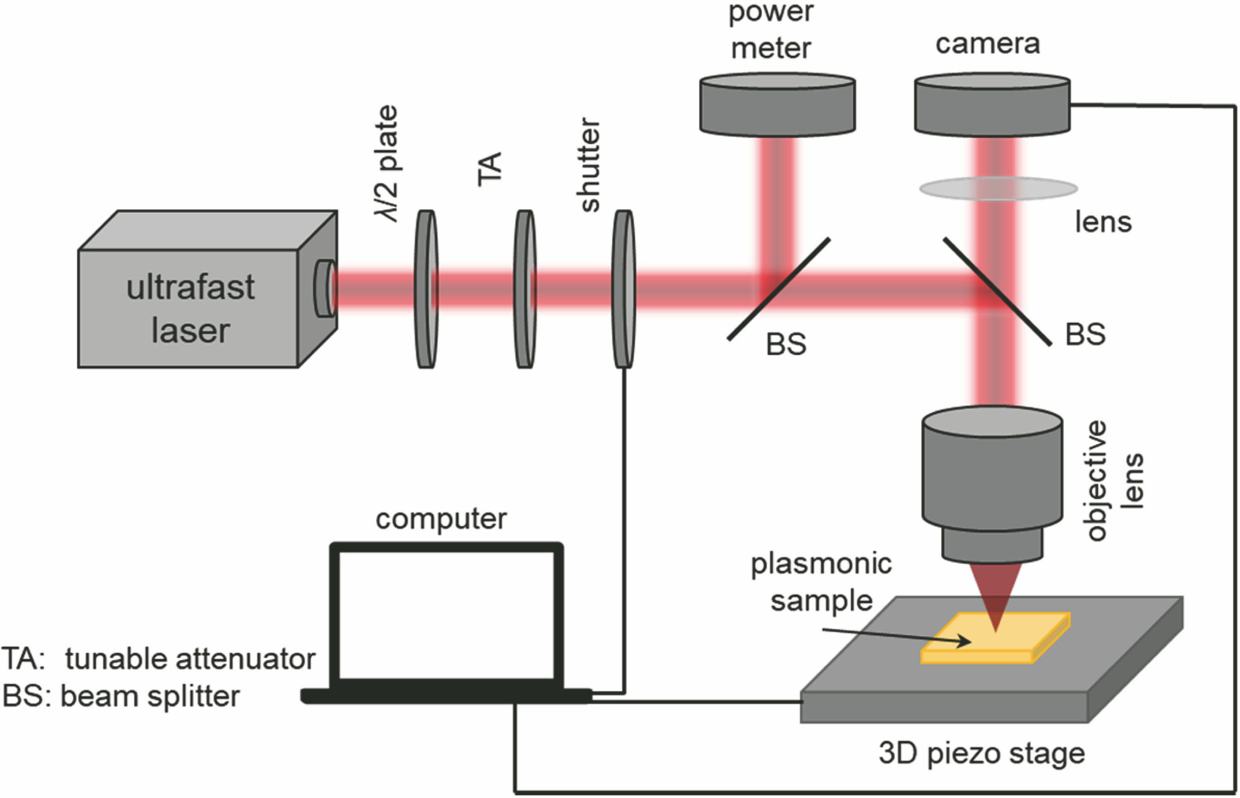
Fig. 1. Schematic of ultrafast laser direct writing system
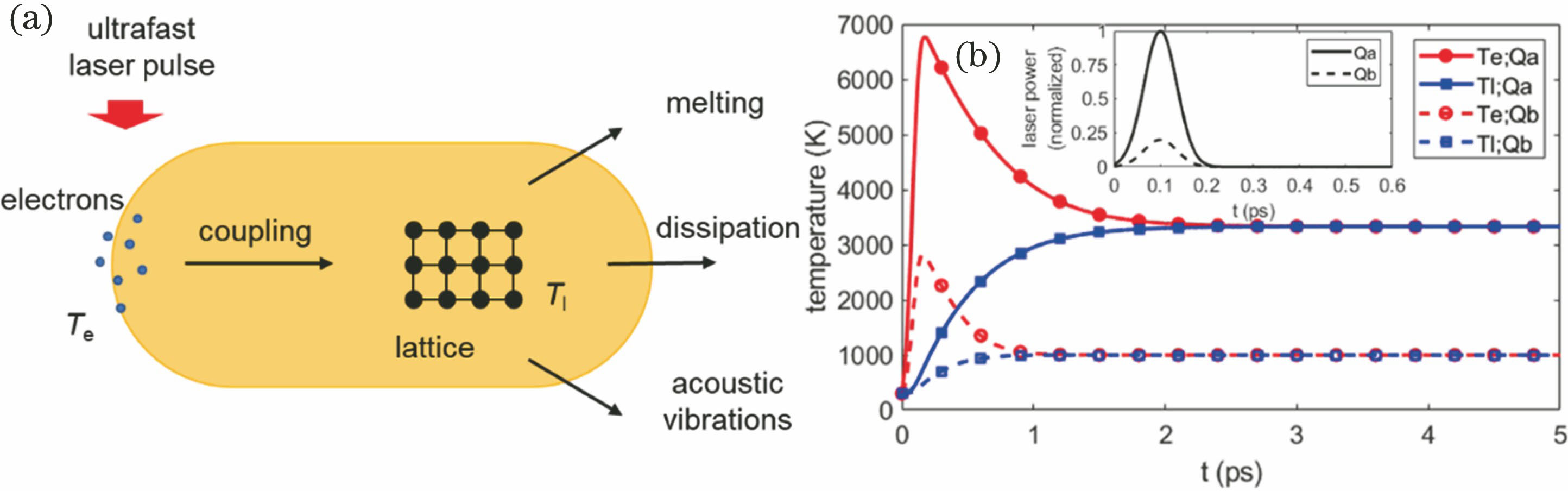
Fig. 2. Schematic of two temperature model (TTM) for plasmonic materials. (a) Schematic of excitation and relaxation of electrons and lattice; (b) variations of electron temperature Te and lattice temperature Tl with time obtained by simulation after fetosecond laser heating with power densities of Qa and Qb (Qa>Qb)
Fig. 3. Schematic of melting above threshold. (a) Schematic for the structural transformation from gold nanorod to nanosphere[30]; (b)TEM image of gold nanorod[31]; (c) TEM image of gold nanosphere[31]; (d) absorption spectrum of gold nanorod[32]; (e) absorption spectrum of gold nanosphere[![Schematics of thermal reshaping and photothermal reshaping[34]. (a) Simulated thermal reshaping evolution of nanorods at constant temperature of 430 K; (b) aspect ratio of Au nanorods in thermal reshaping; (c) thermal reshaping evolution of an gold nanorod by a 150 fs pulse width laser irradiation; (d) photothermal reshaping trajectory with respect to time; (e) final aspect ratio and SEM images vs absorbed energy density after laser pulse irradia](/Images/icon/loading.gif)
Fig. 4. Schematics of thermal reshaping and photothermal reshaping[34]. (a) Simulated thermal reshaping evolution of nanorods at constant temperature of 430 K; (b) aspect ratio of Au nanorods in thermal reshaping; (c) thermal reshaping evolution of an gold nanorod by a 150 fs pulse width laser irradiation; (d) photothermal reshaping trajectory with respect to time; (e) final aspect ratio and SEM images vs absorbed energy density after laser pulse irradia
Fig. 5. Schematics of surface melting for gold nanoparticles [35]. (a) SEM images of gold nanoparticles after surface melting; (b) absorption spectra recorded before and after single-pulse laser heating with various laser energies; (c)(d)(e) schemes for laser-induced size reduction of gold nanoparticles, three possibilities are considered
Fig. 6. Schematic of classical short-pulse laser-matter interaction[36]. (a) Mechanism of classical short-pulse laser-matter interaction; (b) classical short-pulse laser ablation temperature model; (c) laser ablated metal film by 80 μs pump beam with different pulses; (d) laser ablated metal film by 60 ns pulses with different pulses
Fig. 7. Schematic of ultrafast beam-matter interaction[36]. (a) Mechanism of ultrafast beam-matter interaction; (b) two-temperature model as basis of ultrafast ablation model; (c) laser ablated metal film by 10 ps pump beam with different pulses; (d) laser ablated metal film by 170 fs pump beam with different pulses
Fig. 8. Five-dimensional optical data storage based on coding gold nanorod[15]. (a) Schematic of writing progress; (b) schematic of reading progress
Fig. 9. Three-dimensional polarization encoding[16]. (a) Schematic illustration of randomly aligned gold nanorods and the focal polarization with angles θ and β; (b) orientation-unlimited selective excitation and melting of gold nanorods from three-dimensional orientation polarized light; (c) demonstration of 3D orientation-unlimited polarization encryption of five patterns
Fig. 10. Colour printing on nanoimprinted plasmonic metasurfaces using laser post-writing[21]. (a) Schematic illustrations of laser printing governed by photothermal reshaping; (b) measured spectra, corresponding color and SEM images of samples printed under laser dosage from 0 to 535 nJ for single-pulse; (c) illustrations and examples of laser printing on samples without (left) and with (right) polymer coating; (d) laser printing on large and flexible sa
Fig. 11. Schematic illustrations of the near-percolation plasmonic reflector arrays[22]. (a) Schematic of Au-SiO2-Au structure fabrication and SEM images of Au nanoparticles with different colors; (b)(c) samples printed by x and y polarized lasers; (d)(e) optical reflectance spectra of samples printed by x and y polarized lasers with different powers
Fig. 12. Concept of full-visible multifunctional metasurfaces by anisotropic laser printing [23]. (a) Schematic illustration of Al-SiO2-Al structures and polarization selective photothermal reshaping; (b) SEM images of reshaped Al cross nanostructures by a horizontal polarization femtosecond pulse with different laser fluences; (c) measured reflectance specrta and optical images of different Al cross nanostructures at parallel polarization and
Fig. 13. Schematic illustration of on-chip steganography in angular anisotropy nanovolcanoes[25]. (a) SEM images of samples processed at different fluences; (b) simulated and experimental scattering spectra; (c) angularly anisotropic color appearances as a function of the incident angle; (d) the nanovolcano and nanocrater under dark-field objective lenses with different incident angles; (e) sketch of angular steganography under dark-field lenses
Fig. 14. Schematic illustration of nanocrater regulated ratiometric upconversion nanoparticles (UCNPs) emission[26]. (a) Schematics, SEM images and resonance peaks of the nanocraters processed by the laser with different powers; (b) upconversion luminescence spectra from UCNPs deposited on different nanocraters substrates under a 980 nm continuous-wave laser excitation, the insets illustrate the luminous principle; (c) SEM images of UCNPs and decoding of

Set citation alerts for the article
Please enter your email address
© Copyright 2018-2021 | Chinese Laser Press. All Rights Reserved 沪ICP备15018463号-20