• Journal of Semiconductors
  • Vol. 41, Issue 1, 011701 (2020)
Yanbin Huang1、2、3, Jun Liu1、2, Yanchun Deng1、2、4, Yuanyuan Qian1、2、5, Xiaohao Jia1、2, Mengmeng Ma1、2, Cheng Yang1、2, Kong Liu1、2, Zhijie Wang1、2, Shengchun Qu1、2, and Zhanguo Wang1、2
Author Affiliations
  • 1Key Laboratory of Semiconductor Materials Science, Beijing Key Laboratory of Low Dimensional Semiconductor Materials and Devices, Institute of Semiconductors, Chinese Academy of Sciences, Beijing 100083, China
  • 2Center of Materials Science and Optoelectronics Engineering, University of Chinese Academy of Sciences, Beijing 100049, China
  • 3School of Mathematical Science and Engineering, Hebei University of Engineering, Handan 056038, China
  • 4College of Environmental Science and Engineering, Beijing Forestry University, Beijing 100083, China
  • 5Anhui Key Laboratory of Chemo/Biosensing, College of Chemistry and Materials Science, Anhui Normal University, Wuhu 241002, China
  • show less
    DOI: 10.1088/1674-4926/41/1/011701 Cite this Article
    Yanbin Huang, Jun Liu, Yanchun Deng, Yuanyuan Qian, Xiaohao Jia, Mengmeng Ma, Cheng Yang, Kong Liu, Zhijie Wang, Shengchun Qu, Zhanguo Wang. The application of perovskite materials in solar water splitting[J]. Journal of Semiconductors, 2020, 41(1): 011701 Copy Citation Text show less
    (Color online) (a) Schematic structure of cubic ABX3 perovskite unit cell, and (b) the extended tridimensional structure of perovskites formed by the corner-linked octahedral.
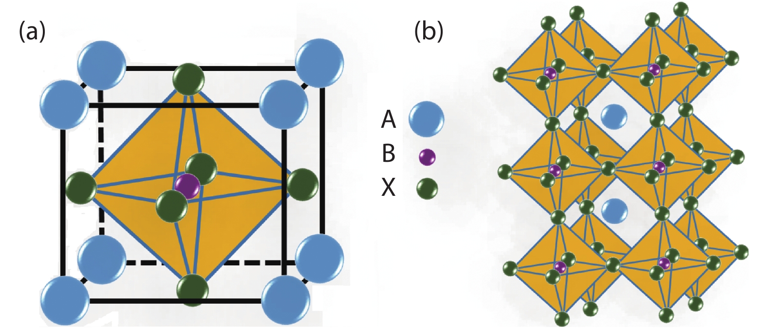
    Fig. 1. (Color online) (a) Schematic structure of cubic ABX3 perovskite unit cell, and (b) the extended tridimensional structure of perovskites formed by the corner-linked octahedral.
    (Color online) Schematic illustration of the basic reaction mechanism of the overall water splitting on a semiconductor (a), and uphill reaction process of photocatalytic water splitting (b). Reprinted from Ref. [44].
    Fig. 2. (Color online) Schematic illustration of the basic reaction mechanism of the overall water splitting on a semiconductor (a), and uphill reaction process of photocatalytic water splitting (b). Reprinted from Ref. [44].
    (Color online) (a) Schematic illustration of water splitting using a TiO2 photoelectrode. Reprinted from Ref. [44]. (b) H-type glass container for the separate evolution of H2 and O2 using a TiO2 thin film photocatalyst device (TiO2 side, 1.0 M NaOH aqueous solutions; Pt side, 0.5 M H2SO4 aqueous solution). Reprinted from Ref. [54].
    Fig. 3. (Color online) (a) Schematic illustration of water splitting using a TiO2 photoelectrode. Reprinted from Ref. [44]. (b) H-type glass container for the separate evolution of H2 and O2 using a TiO2 thin film photocatalyst device (TiO2 side, 1.0 M NaOH aqueous solutions; Pt side, 0.5 M H2SO4 aqueous solution). Reprinted from Ref. [54].
    (Color online) Schematic illustration of the main processes of the photocatalytic overall water splitting reaction.
    Fig. 4. (Color online) Schematic illustration of the main processes of the photocatalytic overall water splitting reaction.
    (Color online) Schematic illustration of (a) the band structure and (b) DOS (density of states) plots of LCTO, (c) typical time course of photocatalytic H2 evolution reaction, (d) photocatalytic O2 evolution rate as a function of the cutoff wavelength of incident light. Reprinted from Ref. [69].
    Fig. 5. (Color online) Schematic illustration of (a) the band structure and (b) DOS (density of states) plots of LCTO, (c) typical time course of photocatalytic H2 evolution reaction, (d) photocatalytic O2 evolution rate as a function of the cutoff wavelength of incident light. Reprinted from Ref. [69].
    (Color online) (a) Schematic diagram of band positions relative to the vacuum level and NHE for the BFO50-STO50 film. A, B, and C represent the photoexcited carriers relaxation and recombination processes. (b) Current density-potential curves of BFO, BFO75-STO25, BFO50-STO50, BFO25-STO75, and STO films. Reprinted from Ref. [81].
    Fig. 6. (Color online) (a) Schematic diagram of band positions relative to the vacuum level and NHE for the BFO50-STO50 film. A, B, and C represent the photoexcited carriers relaxation and recombination processes. (b) Current density-potential curves of BFO, BFO75-STO25, BFO50-STO50, BFO25-STO75, and STO films. Reprinted from Ref. [81].
    (Color online) The morphology engineering strategy for SrTiO3 nanocrystals. (a–c) The morphology of 6-facet SrTiO3 nanocrystals. (d) The structure of the {001} facet of SrTiO3. (e) The schematic description of changing SrTiO3 nanocrystals from 6-facet to 18-facet. (f–h) The morphology of 18-facet SrTiO3 nanocrystals. (i) The structure of the {110} facet of SrTiO3. Reprinted from Ref. [85].
    Fig. 7. (Color online) The morphology engineering strategy for SrTiO3 nanocrystals. (a–c) The morphology of 6-facet SrTiO3 nanocrystals. (d) The structure of the {001} facet of SrTiO3. (e) The schematic description of changing SrTiO3 nanocrystals from 6-facet to 18-facet. (f–h) The morphology of 18-facet SrTiO3 nanocrystals. (i) The structure of the {110} facet of SrTiO3. Reprinted from Ref. [85].
    (Color online) (a) UV–vis absorption spectra and (b) typical time course of photocatalytic H2 evolution reaction of c-NaNbO3 (cubic NaNbO3) and o-NaNbO3 (orthorhombic NaNbO3) samples. Reprinted from Ref. [31].
    Fig. 8. (Color online) (a) UV–vis absorption spectra and (b) typical time course of photocatalytic H2 evolution reaction of c-NaNbO3 (cubic NaNbO3) and o-NaNbO3 (orthorhombic NaNbO3) samples. Reprinted from Ref. [31].
    (Color online) (a) External quantum yield spectra measured for BFO electrodes before poling and after + 8 and –8 V poling. (b) Photocurrent-potential characteristics of the photoelectrodes with different polarization states. Schematic illustrations of the mechanisms in photoexcited charge transfer from BFO films to the electrolyte and from excited surface modifiers to the BFO films after the BFO films were (c) positively and (d) negatively poled. Reprinted from Ref. [99]. (e, f) Schematic electronic band structure and the mechanisms for the injected hot-electron transfer from PZT films to the electrolyte for the two poling configurations. Reprinted from Ref. [101].
    Fig. 9. (Color online) (a) External quantum yield spectra measured for BFO electrodes before poling and after + 8 and –8 V poling. (b) Photocurrent-potential characteristics of the photoelectrodes with different polarization states. Schematic illustrations of the mechanisms in photoexcited charge transfer from BFO films to the electrolyte and from excited surface modifiers to the BFO films after the BFO films were (c) positively and (d) negatively poled. Reprinted from Ref. [99]. (e, f) Schematic electronic band structure and the mechanisms for the injected hot-electron transfer from PZT films to the electrolyte for the two poling configurations. Reprinted from Ref. [101].
    (Color online) Schematic illustration of the (a) electron–hole separation of La2Ti2O7/LaCrO3 heterojunction and (b) g-C3N4/SrTiO3:Rh composite under visible light irradiation. Reprinted from Refs. [111, 113], respectively.
    Fig. 10. (Color online) Schematic illustration of the (a) electron–hole separation of La2Ti2O7/LaCrO3 heterojunction and (b) g-C3N4/SrTiO3:Rh composite under visible light irradiation. Reprinted from Refs. [111, 113], respectively.
    (Color online) (a) Synthesis route of SrTiO3/TiO2 HoMs from hydrothermal reaction. (b) Typical time course of photocatalytic H2 and O2 evolution reaction of triple shelled SrTiO3/TiO2 HoMs photocatalyst. (c) Possible band structure diagram for SrTiO3/TiO2 HoMs. Reprinted from Ref. [118].
    Fig. 11. (Color online) (a) Synthesis route of SrTiO3/TiO2 HoMs from hydrothermal reaction. (b) Typical time course of photocatalytic H2 and O2 evolution reaction of triple shelled SrTiO3/TiO2 HoMs photocatalyst. (c) Possible band structure diagram for SrTiO3/TiO2 HoMs. Reprinted from Ref. [118].
    (Color online) Schematic illustration of (a) the photogenerated charge transfer and catalytic reaction mechanisms of the fabricated LaCoO3/Au nano-composite (Reprinted from Ref. [125]), and (b) the prepared Au/LTO NSP. (c) The diffuse reflectance spectra (left axis, blue line) and apparent quantum efficiency (right axis, red column) of Au-LTO NSP under vis-NIR (λ > 420 nm) light irradiation. Reprinted from Ref. [ 127].
    Fig. 12. (Color online) Schematic illustration of (a) the photogenerated charge transfer and catalytic reaction mechanisms of the fabricated LaCoO3/Au nano-composite (Reprinted from Ref. [125]), and (b) the prepared Au/LTO NSP. (c) The diffuse reflectance spectra (left axis, blue line) and apparent quantum efficiency (right axis, red column) of Au-LTO NSP under vis-NIR (λ > 420 nm) light irradiation. Reprinted from Ref. [ 127].
    (Color online) (a) Schematics and cross-section of scanning electron microscope (SEM) of the fabricated ITO/PZT/Au, ITO/PZT/Au/PZT, and ITO/Au/PZT electrodes. (b) Top-view SEM image of nano-Au array fabricated on ITO glass; scale bar, 1 μm. The inset zooms in one part of the SEM; scale bar, 200 nm. (c) FDTD-simulated spatial distribution of the electric field intensity around the square dot illuminated by 800 nm light. (d) Photocurrent-potential measurements of ITO/nano-Au/PZT(black), ITO/PZT/nano-Au/PZT (red) and ITO/PZT/nano-Au (blue) under the white-light excitation (filtered, > 450 nm). (e) Photocurrent-potential measurements of the ITO/PZT/nano-Au/PZT (the as-grown (black), + 10 V (red) and –10 V (blue) poled) under the white-light excitation (filtered, > 450 nm). Reprinted from Ref. [ 101].
    Fig. 13. (Color online) (a) Schematics and cross-section of scanning electron microscope (SEM) of the fabricated ITO/PZT/Au, ITO/PZT/Au/PZT, and ITO/Au/PZT electrodes. (b) Top-view SEM image of nano-Au array fabricated on ITO glass; scale bar, 1 μm. The inset zooms in one part of the SEM; scale bar, 200 nm. (c) FDTD-simulated spatial distribution of the electric field intensity around the square dot illuminated by 800 nm light. (d) Photocurrent-potential measurements of ITO/nano-Au/PZT(black), ITO/PZT/nano-Au/PZT (red) and ITO/PZT/nano-Au (blue) under the white-light excitation (filtered, > 450 nm). (e) Photocurrent-potential measurements of the ITO/PZT/nano-Au/PZT (the as-grown (black), + 10 V (red) and –10 V (blue) poled) under the white-light excitation (filtered, > 450 nm). Reprinted from Ref. [ 101].
    Yanbin Huang, Jun Liu, Yanchun Deng, Yuanyuan Qian, Xiaohao Jia, Mengmeng Ma, Cheng Yang, Kong Liu, Zhijie Wang, Shengchun Qu, Zhanguo Wang. The application of perovskite materials in solar water splitting[J]. Journal of Semiconductors, 2020, 41(1): 011701
    Download Citation