• Photonics Research
  • Vol. 11, Issue 7, 1275 (2023)
Valerio Vitali1、2、*, Thalía Domínguez Bucio1, Cosimo Lacava2, Riccardo Marchetti3, Lorenzo Mastronardi1, Teerapat Rutirawut1, Glenn Churchill1, Joaquín Faneca1、4, James C. Gates1, Frederic Gardes1, and Periklis Petropoulos1
Author Affiliations
  • 1Optoelectronics Research Centre, University of Southampton, Southampton, SO17 1BJ, UK
  • 2Electrical, Computer and Biomedical Engineering Department, University of Pavia, 27100 Pavia, Italy
  • 3Advanced Fiber Resources Milan S.r.l., 20098 San Donato Milanese, Italy
  • 4Currently at Instituto de Microelectrónica de Barcelona, IMB-CNM (CSIC), Campus UAB, 08193 Bellaterra, Spain
  • show less
    DOI: 10.1364/PRJ.488970 Cite this Article Set citation alerts
    Valerio Vitali, Thalía Domínguez Bucio, Cosimo Lacava, Riccardo Marchetti, Lorenzo Mastronardi, Teerapat Rutirawut, Glenn Churchill, Joaquín Faneca, James C. Gates, Frederic Gardes, Periklis Petropoulos. High-efficiency reflector-less dual-level silicon photonic grating coupler[J]. Photonics Research, 2023, 11(7): 1275 Copy Citation Text show less
    (a) 2D schematic view and simulation layout of the proposed dual-level Si GC; (b) cross-sectional schematic with the parameter names used to indicate the GC dimensions.
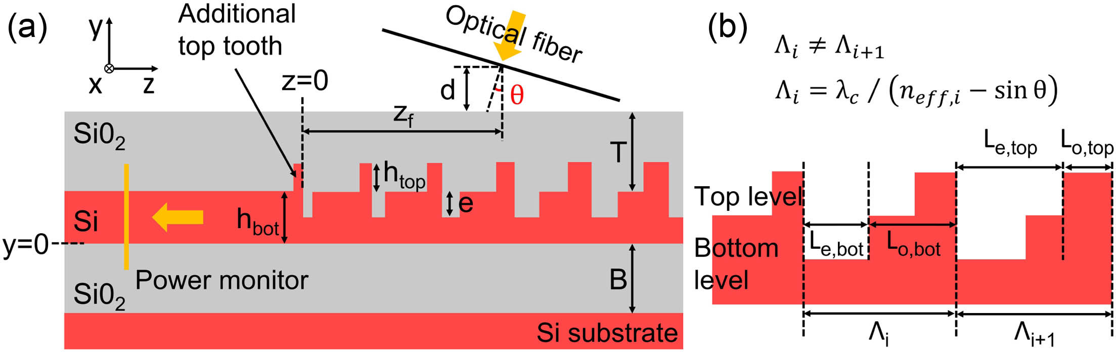
    Fig. 1. (a) 2D schematic view and simulation layout of the proposed dual-level Si GC; (b) cross-sectional schematic with the parameter names used to indicate the GC dimensions.
    (a) 2D numerical simulations of the CE at 1550 nm as a function of the bottom linear apodization factor Rbot and the etching depth e considering a single-level GC with a waveguide thickness hbot=220 nm. Other parameters used in the simulations are B=2 μm, Fin,bot=0.9, θ=14.5°, and T=720 nm. (b) 3D numerical simulations of the CE as a function of wavelength for the best-performing single-level and dual-level GC considering hbot=220 nm.
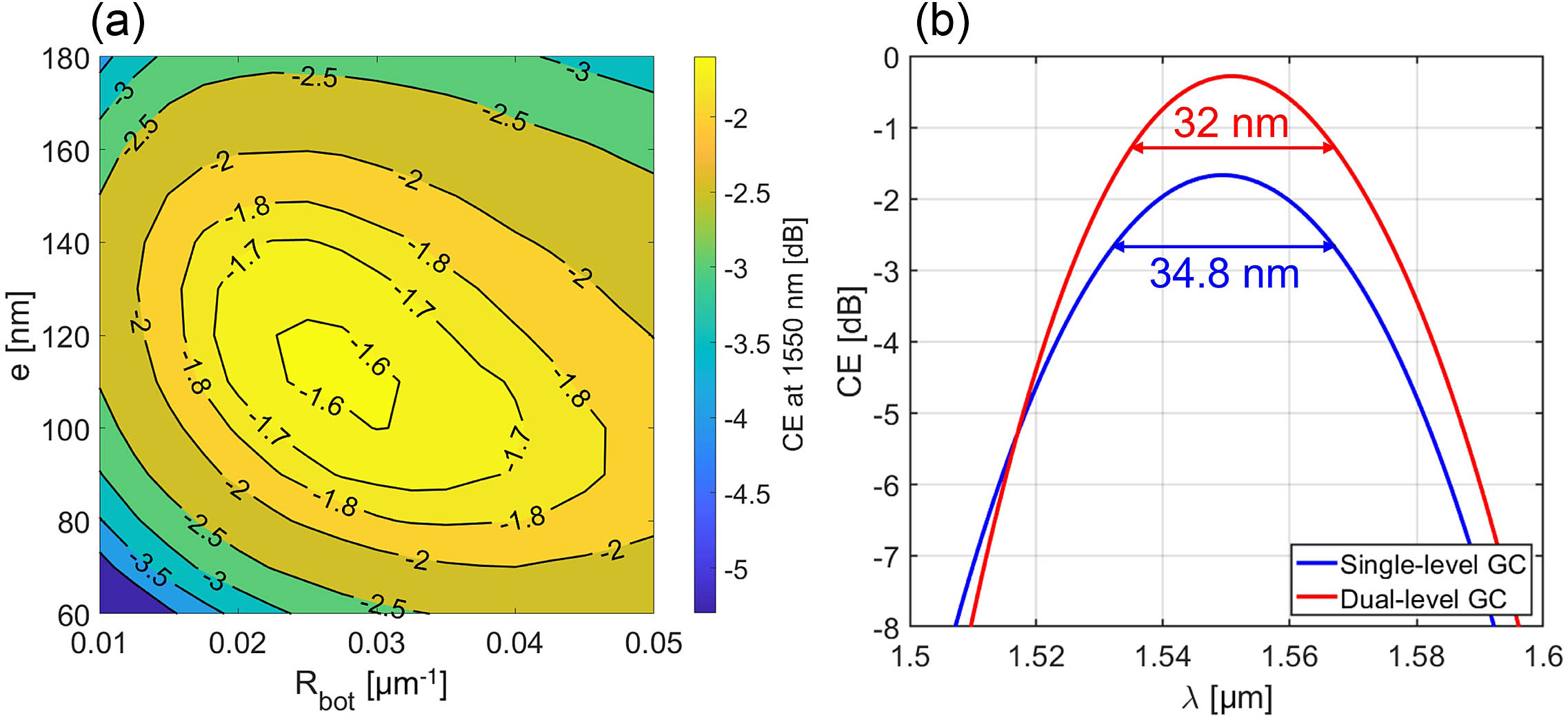
    Fig. 2. (a) 2D numerical simulations of the CE at 1550 nm as a function of the bottom linear apodization factor Rbot and the etching depth e considering a single-level GC with a waveguide thickness hbot=220  nm. Other parameters used in the simulations are B=2  μm, Fin,bot=0.9, θ=14.5°, and T=720  nm. (b) 3D numerical simulations of the CE as a function of wavelength for the best-performing single-level and dual-level GC considering hbot=220  nm.
    2D numerical simulations of (a) directionality and (b) CE at 1550 nm as a function of the top linear apodization factor Rtop and thickness of the top level htop for a dual-level GC with hbot=220 nm. Other parameters used in the simulations are e=110 nm, Rbot=0.0275 μm−1, B=2 μm, Fin,bot=0.9, Fin,top=0.1, θ=14.5°, and T=720 nm.
    Fig. 3. 2D numerical simulations of (a) directionality and (b) CE at 1550 nm as a function of the top linear apodization factor Rtop and thickness of the top level htop for a dual-level GC with hbot=220  nm. Other parameters used in the simulations are e=110  nm, Rbot=0.0275  μm1, B=2  μm, Fin,bot=0.9, Fin,top=0.1, θ=14.5°, and T=720  nm.
    Fabrication process diagram for the dual-level GC: (a) starting from SOI wafer with a Si thickness of 340 nm; (b) bottom GC level etching; (c) top GC level etching; (d) waveguide etching; (e) SiO2 cladding deposition. (f) Top-view and (g) angled-view SEM images of a fabricated device.
    Fig. 4. Fabrication process diagram for the dual-level GC: (a) starting from SOI wafer with a Si thickness of 340 nm; (b) bottom GC level etching; (c) top GC level etching; (d) waveguide etching; (e) SiO2 cladding deposition. (f) Top-view and (g) angled-view SEM images of a fabricated device.
    Simulated (red curve) and experimentally measured (blue curve) CE as a function of wavelength for the fabricated dual-level GC with a bottom waveguide thickness hbot=220 nm and top-level thickness htop=120 nm.
    Fig. 5. Simulated (red curve) and experimentally measured (blue curve) CE as a function of wavelength for the fabricated dual-level GC with a bottom waveguide thickness hbot=220  nm and top-level thickness htop=120  nm.
    (a) Peak CE (CEpeak, left y axis) and peak wavelength (λpeak, right y axis) as a function of the mask misalignment; variation of the dimensions of the first top tooth and first bottom trench in the cases of (b) aligned masks, (c) −30 nm mask misalignment, and (d) +30 nm mask misalignment.
    Fig. 6. (a) Peak CE (CEpeak, left y axis) and peak wavelength (λpeak, right y axis) as a function of the mask misalignment; variation of the dimensions of the first top tooth and first bottom trench in the cases of (b) aligned masks, (c) 30  nm mask misalignment, and (d) +30  nm mask misalignment.
    Si [nm]DescriptionCES [dB]CEE [dB]Ref.Si [nm]DescriptionCES [dB]CEE [dB]Ref.
    220GA*−2.15[15]220GA*−1.9[16]
    220GA + DBR*−0.36[15]220bDual-level−0.28−0.8This work
    220Poly-Si overlay−1.08[17]250Full-etch PhC−1.8−1.74[18]
    220Poly-Si overlay*−1.6[19]250Lag effect etch*−1.31−1.9[20]
    220Linear apodiz.−2.6−2.7[21]250Linear apodiz.−2.2−2.7[22]
    220Gold BR−1.43−1.61[23]250Aluminum BR*−0.33−0.5[24]
    220DBR*−0.86−1.58[25]250Aluminum BR*−0.33−0.62[26]
    220Linear apodiz.−1.6[27]250Aluminum BR−0.43−0.58[28]
    220DBR*−1.02[29]260Linear apodiz.−0.8−0.9[27]
    220Si overlay*−1.8−2.6[30]260GA*−1.0[16]
    220Ge overlay−1.19[31]300Dual-etch−0.25[32]
    220Dual-etch−1.24−2.2[33]300Dual-etch−2.2−2.7[34]
    220Dual-etch−1.05[35]340GA*−0.5[16]
    220Dual-etch−1.1−1.3[36]340Apodized GC−0.76−1.2[37]
    220Aluminum BR−0.67−0.69[38]340Apodized GC−1[39]
    220SWG+prism−0.5−1.0[40]340Apodized GC*−0.7[39]
    Table 1. Summary of the Best Numerically Simulated (CES) and Experimentally Measured (CEE) Coupling Efficiencies Reported in the Literature for Different GCs in the C-Telecom Banda
    No.Λ[nm]Lo,bot[nm]Lo,top[nm]No.Λ[nm]Lo,bot[nm]Lo,top[nm]
    16105496113643434161
    26135406914646424170
    36165327715649413179
    46185228516652402188
    56215139317656392198
    662350310118659381208
    762649410919662369217
    862948411720665358227
    963247512621669347237
    1063546513422672335247
    1163745414323675323257
    1264044415224679311268
    Table 2. Optimal Dimensions (Common Period Λ, Bottom Tooth Width Lo,bot, and Top Tooth Width Lo,top) Obtained from the Optimization of the Apodized Dual-Level Si GC with Waveguide Thickness hbot = 220 nm and Top Level Thickness htop = 120 nma
    Valerio Vitali, Thalía Domínguez Bucio, Cosimo Lacava, Riccardo Marchetti, Lorenzo Mastronardi, Teerapat Rutirawut, Glenn Churchill, Joaquín Faneca, James C. Gates, Frederic Gardes, Periklis Petropoulos. High-efficiency reflector-less dual-level silicon photonic grating coupler[J]. Photonics Research, 2023, 11(7): 1275
    Download Citation