We present the design and experimentally demonstrate a dual-level grating coupler with subdecibel efficiency for a 220 nm thick silicon photonics waveguide which was fabricated starting from a 340 nm silicon-on-insulator wafer. The proposed device consists of two grating levels designed with two different linear apodizations, with opposite chirping signs, and whose period is varied for each scattering unit. A coupling efficiency of at 1550 nm is experimentally demonstrated, which represents the highest efficiency ever reported in the telecommunications C-band in a single-layer silicon grating structure without the use of any backreflector or index-matching material between the fiber and the grating.
1. INTRODUCTION
Silicon photonics leverages the mature and monolithic processing techniques inherited from microelectronics to achieve the fabrication of highly integrated optical chips at a wafer-scale level [1,2]. Thanks to the strong refractive index contrast between the Si core ( at 1550 nm) and the cladding ( at 1550 nm) achieved in the silicon-on-insulator (SOI) platform, single-mode waveguides with tight bending radii [3,4] can be fabricated. As a result, and because of the SOI compatibility with CMOS processes and the possibility to fabricate low-cost and high-performance optical devices, interest in silicon photonics has continued to grow and covers a wide range of research fields including all-optical processing [5,6], sensing [7,8], metrology [9], and quantum technologies [10,11]. However, an important challenge that remains in silicon photonics is the efficient fiber-to-chip coupling, which originates from the significant dimension difference between the optical fiber [with a mode field diameter (MFD) of 10.4 μm for a standard single-mode fiber (SMF-28)] and the integrated SOI waveguides (which have a typical cross section of ) [12].
To tackle this challenge, the two most widely adopted solutions are based on the use of edge couplers (ECs) and grating couplers (GCs). ECs enable remarkably low coupling losses ( is achievable) over a wide wavelength range () and can be realized using different configurations such as inverse tapers, multi-layer structures [13], or subwavelength grating metamaterial mode expanders [14] located at the chip facets. Although this approach is effective in achieving a high coupling efficiency (CE), it is not suitable for wafer-scale automated testing and high-volume production, since ECs require accurate post-fabrication processes, such as high-quality polishing of the chip facets and precise optical alignment. Conversely, GCs represent a better coupling interface for rapid wafer-scale testing because they can be fabricated anywhere on the chip surface and are characterized by much more relaxed alignment tolerances compared to those achievable using ECs [12]. However, standard uniform grating couplers (UGCs) typically show a narrow 1 dB bandwidth (BW) (usually in the range of 30–40 nm) and poor CE, which is usually lower than [12]. Several design and fabrication techniques have been reported in the literature to overcome this limit and increase the CE of SOI GCs, whose best results in the telecommunications C-band are summarized in Table 1.
Summary of the Best Numerically Simulated (CES) and Experimentally Measured (CEE) Coupling Efficiencies Reported in the Literature for Different GCs in the C-Telecom Banda
Si [nm]
Description
[dB]
[dB]
Ref.
Si [nm]
Description
[dB]
[dB]
Ref.
220
GA*
−2.15
–
[15]
220
GA*
−1.9
–
[16]
220
GA + DBR*
−0.36
–
[15]
220b
Dual-level
−0.28
−0.8
This work
220
Poly-Si overlay
−1.08
–
[17]
250
Full-etch PhC
−1.8
−1.74
[18]
220
Poly-Si overlay*
–
−1.6
[19]
250
Lag effect etch*
−1.31
−1.9
[20]
220
Linear apodiz.
−2.6
−2.7
[21]
250
Linear apodiz.
−2.2
−2.7
[22]
220
Gold BR
−1.43
−1.61
[23]
250
Aluminum BR*
−0.33
−0.5
[24]
220
DBR*
−0.86
−1.58
[25]
250
Aluminum BR*
−0.33
−0.62
[26]
220
Linear apodiz.
−1.6
–
[27]
250
Aluminum BR
−0.43
−0.58
[28]
220
DBR*
−1.02
–
[29]
260
Linear apodiz.
−0.8
−0.9
[27]
220
Si overlay*
−1.8
−2.6
[30]
260
GA*
−1.0
–
[16]
220
Ge overlay
−1.19
–
[31]
300
Dual-etch
−0.25
–
[32]
220
Dual-etch
−1.24
−2.2
[33]
300
Dual-etch
−2.2
−2.7
[34]
220
Dual-etch
−1.05
–
[35]
340
GA*
−0.5
–
[16]
220
Dual-etch
−1.1
−1.3
[36]
340
Apodized GC
−0.76
−1.2
[37]
220
Aluminum BR
−0.67
−0.69
[38]
340
Apodized GC
–
−1
[39]
220
SWG+prism
−0.5
−1.0
[40]
340
Apodized GC*
–
−0.7
[39]
The symbol * in the Description columns indicates the use of an index-matching material between the fiber and the GC.
220 nm thick Si waveguide fabricated starting from a 340 nm SOI wafer.
In general, the CE is proportional to the GC directionality (defined as the percentage of the optical power that is scattered from the direction of the waveguide and GC upwards toward the optical fiber) and GC-fiber mode matching, and inversely proportional to the reflectivity at the waveguide–GC interface. Directionality enhancement can be achieved by employing different techniques, such as a staircase design with dual- or multi-etching depths [32,34,41] or the use of poly-silicon [17,19,42] or germanium (Ge) [31] over-layers. For example, CE values as high as [43] and [44] in devices designed for 1200 nm and 1300 nm, respectively, were experimentally demonstrated using a bi-layer GC with a poly-silicon overlay and a 5 μm MFD lensed fiber. Another common approach to increase the GC directionality is the use of backreflectors (BRs) embedded in the substrate, either based on metallic mirrors [23,24,26,28,38] or distributed Bragg reflectors (DBRs) [15,25]. As can be seen from Table 1, GCs with embedded BRs typically outperform all other solutions in the telecom C-band. However, this approach presents some limitations and difficulties from a fabrication perspective. Regarding the use of metallic mirrors, the fabrication of metal BRs may require the adoption of non-CMOS compatible materials which can be unviable in a metal-free fabrication environment [28]. As for DBRs, they can be fabricated using a stack of several amorphous Si and layers, but this requires additional fabrication steps and may result in low fabrication tolerances and large difference from the simulated performance [25]. Therefore, GC designs that do not require the use of BRs are generally preferable.
Sign up for Photonics Research TOC. Get the latest issue of Photonics Research delivered right to you!Sign up now
An effective way to increase the CE is the application of an apodization profile, which can tailor the amount of power scattered by each grating period so as to decrease the mode mismatch between the field profile radiated by the GC and the Gaussian-like fiber mode. Apodization also results in a reduction of the backreflection at the waveguide–GC interface. It is typically performed by varying either the fill factor of each period [15–17,21,22,26–28,37,45] or the etching depth [20]. Two main design strategies are usually employed, and sometimes combined, to perform a GC apodization. In the first approach, numerical simulations, commonly based on genetic algorithms, are used to define the apodization profile by maximizing a specific figure of merit (generally the CE) [26]. The second approach makes use of analytical expressions to tailor the apodization profile and match the power-distribution profile of the optical fiber. An example is the use of a linear apodization, in which one of the GC parameters (e.g., the fill factor) is linearly chirped while keeping the other parameters constant (or modifying them accordingly) [27]. In addition to these techniques, to avoid loss of power due to reflections at the air interface, an index-matching material between the fiber and the GC can be used, which typically results in a CE increase of about 0.3 dB [24,39].
In this work, we propose and experimentally demonstrate an apodized dual-level GC for a 220 nm thick SOI platform with a measured CE of . To the best of our knowledge, this represents the highest CE ever achieved in the telecommunications C-band for SOI GCs without the use of any BR or index-matching material between the fiber and the grating. The proposed structure consists of two grating levels where two different linear apodizations, with opposite signs, are applied. The bottom and top gratings have the same period, whose value is varied for each scattering unit to ensure that the Bragg condition is satisfied along the entire GC length. The GC was fabricated starting from a 340 nm thick SOI wafer by means of two etching steps, which allowed achieving a dual-level configuration without the need of depositing an additional poly-Si overlay. An additional etching step was performed to define single-mode waveguides and linear tapers to connect two GCs together to allow their characterization. Thanks to its versatility, the presented design strategy can in principle be applied to any SOI thickness or other integrated photonic platforms.
2. GRATING COUPLER LAYOUT
In standard UGCs, trenches with a fixed length and constant etching depth are etched in the Si waveguide with a period . By defining the grating fill factor as the ratio between the tooth length (the un-etched section of the period) and the total length of the scattering unit, it is possible to express the effective refractive index of the GC as follows: where and are the effective refractive indices of the original Si slab and the etched section, respectively. The periodic variation in the effective refractive index between the trenches and the un-etched teeth results in the diffraction of the optical mode propagating in the Si waveguide to free space at a certain angle. According to the first-order Bragg condition, the GC period can be calculated as where is the coupling wavelength and is the diffraction angle in air. As previously mentioned, a linear apodization of the factor can help increase the CE thanks to an improvement in the GC-fiber mode matching and a reduction in the optical impedance mismatch between the waveguide and the grating section [16]. In most of the linearly apodized GC demonstrations reported in the literature, is kept constant along the whole grating length [16,21,22]. As we discussed in our previous work [27], this approach does not allow for the Bragg condition to be simultaneously satisfied by all of the scattering units: as the parameter is varied along the GC, the effective refractive index of each grating element changes, and therefore the Bragg law is satisfied only at a specific position of the GC but not along its whole length. To mitigate this issue, we proposed a new design methodology based on the simultaneous linear apodization of and a corresponding variation of along the GC length, so as to satisfy the Bragg condition along the whole structure.
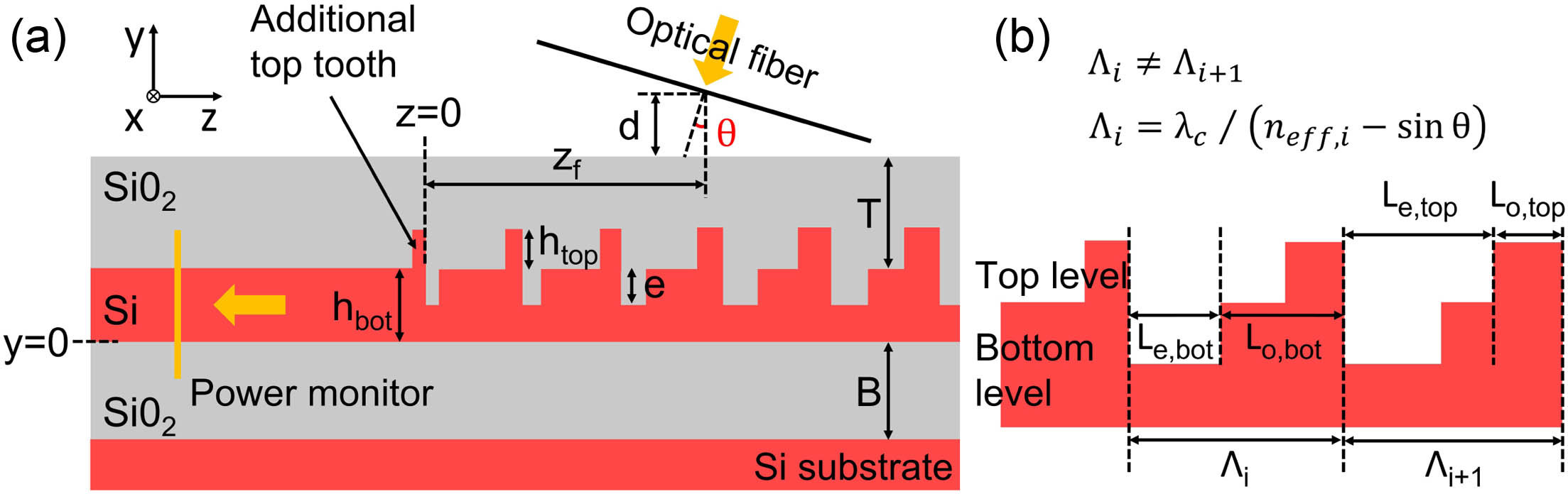
While keeping these considerations into account, the design we present in this work aims at further improving the CE by maximizing the GC directionality. The schematic layout of the apodized dual-level SOI GC proposed here is shown in Figs. 1(a) and 1(b). The bottom level, which acts as the light guiding level, has a thickness and an etching depth , while the top GC level has a thickness and is fully etched. For each radiative unit, the two GC levels have the same period and their teeth are aligned on the furthermost border. The fill factors of the two levels are defined by two linear apodization functions, with opposite chirping signs. This architecture ensures that the design objective of increasing directionality is achieved, while facilitating the reduction of the mode mismatch thanks to the GC apodization. The following expression is used to apodize the bottom GC: in which is the initial fill factor of the first bottom radiative unit, stands for the bottom linear apodization factor, and is the distance of each radiative unit from the start of the GC. The starting position of the GC is indicated by in Fig. 1(a), while the end point corresponds to the last period of the GC (not shown in the figure). In a similar way, the equation used to define the apodization of the top level is the following: in which is the initial fill factor of the first top radiative unit and stands for the top linear apodization factor. An additional tooth in the top level, whose width was set equal to the minimum dimension achievable in our fabrication process (60 nm), is added before the first GC period to increase the CE, as already discussed in Refs. [45–47].
Figure 1.(a) 2D schematic view and simulation layout of the proposed dual-level Si GC; (b) cross-sectional schematic with the parameter names used to indicate the GC dimensions.
The adoption of two linear apodizations with opposite signs for the two levels has two main benefits: the first is that it allows minimizing the backreflection at the GC interface and the mismatch between the bottom Si mode and the composite dual-level GC mode [45]. The second benefit is that it reduces the space of simulation variables: since the values of and are constrained by the minimum feature dimension achievable in fabrication and the common period is recalculated for each scattering unit using Eqs. (1)–(3), the tooth and trench lengths for both levels are defined only by two variables, namely and . This allows exploring a broad variable space and a large number of possible GC configurations by simultaneously varying the dimensions of both levels; this is in contrast to previously reported designs where each grating period and fill factor were optimized independently [46]. Considering a thickness of for the bottom Si level and μ for the bottom layer, the other free GC parameters to be optimized are , , and the thickness of the top cladding (TOX) . A standard SMF-28 optical fiber was considered, with an outer diameter of 125 μm and an MFD of 10.4 μm at 1550 nm. The angle of incidence was set equal to 14.5° with respect to the vertical direction to help reduce any backreflections into the fiber [27]. The point of the optical fiber closest to the TOX surface was set at a distance of 0.5 μm, corresponding to a distance between the center of the optical fiber core and the TOX surface μ for [see Fig. 1(a)]. Therefore, the only fiber parameter to be optimized is the offset , i.e., the distance of the central position of the fiber to the start of the GC.
3. DESIGN METHODOLOGY AND SIMULATIONS
The design of the dual-level GC was carried out in three steps. In the first step, only the bottom GC level was considered [setting referring to Fig. 1(a)]: a linear apodization of the fill factor was applied [see Eq. (3)] and was varied along the whole structure to satisfy the Bragg condition for in each point of the GC. Concerning the choice of , it has been shown that increasing its value (and, thus, decreasing the first bottom trench width), results in an increase in the grating CE [22]. Considering a minimum feature size of 60 nm, which is compatible with the use of E-beam lithography, we set the value of equal to 0.9. The optimal values for and that maximize the CE of the bottom GC were then found by performing a set of full vectorial 2D-FDTD simulations using FDTD Solutions (from ANSYS Inc.). Specifically, the CE was calculated by modeling the GC as an in-coupling device, i.e., coupling power from the fiber into the SOI waveguide by means of the grating [see the simulation layout of Fig. 1(a), considering for this first design step]. The electric field polarization of the Gaussian beam was set along the direction, which resulted in the incoming optical power being coupled to the fundamental TE mode of the SOI waveguide. A frequency-domain power monitor was used to calculate the total power coupled in the fundamental TE waveguide mode and, hence, the grating CE. For each value of the pair of parameters, the value of the fiber offset was also optimized. This was performed by sweeping from 3 to 10 μm at 0.2 μm steps for each combination of the pair of parameters and by selecting the fiber offset value maximizing the GC CE. The results of the parameter sweep for the bottom GC level with are reported in Fig. 2(a), which shows a contour plot of the peak CE at 1550 nm as a function of the and parameters. A maximum CE equal to can be achieved by setting and μ, with the optimized fiber offset value equal to 6.2 μm. A full vectorial 3D-FDTD simulation was then performed on the optimum single-level GC to account for the grating width and verify the GC performance. Figure 2(b) shows the resulting CE as a function of wavelength for the optimized single-level GC considering a grating width in the direction of 14 μm, with a peak CE at 1550 nm of and a 1 dB BW of 34.8 nm.
Figure 2.(a) 2D numerical simulations of the CE at 1550 nm as a function of the bottom linear apodization factor and the etching depth considering a single-level GC with a waveguide thickness . Other parameters used in the simulations are μ, , , and . (b) 3D numerical simulations of the CE as a function of wavelength for the best-performing single-level and dual-level GC considering .
A major factor contributing to the CE reported above for the optimum single-level GC is the directionality of the grating, which was calculated to be equal to 72.6% at 1550 nm. To address this, in the second design step, the top grating level was added and its impact on the overall GC performance was investigated. The parameters of the bottom grating were set equal to those of the optimum configuration found in the first step. A linear apodization of the fill factor, with a chirping sign opposite to the one of the bottom level, was applied to the top level [see Eq. (4)]. In order to minimize the mode mismatch between the waveguide mode and the dual-level GC mode, a small dimension for the first top tooth is required [45]. Therefore, by considering a smallest feature of 60 nm as before, the value of was set to 0.1. Since the top level is fully etched and has the same period as the bottom grating for each scattering element, the only two top GC parameters that need to be optimized are and . To get a complete understanding of the effect of these two parameters on the overall performance, the grating was initially simulated as an out-coupling device. A fundamental TE mode source was set in the SOI waveguide and a power monitor was positioned above the GC to evaluate its directionality. Specifically, a 1D horizontal power monitor was placed at μ spanning from μ to μ [see Fig. 1(a) for the Cartesian axes] to collect all of the optical power scattered upwards by the GC. Figure 3(a) shows the directionality of the dual-level GC at 1550 nm as a function of and . As can be seen, the addition of the top level enables directionality values in excess of 96%, showing a significant improvement compared to the case of the best-performing single-level GC (directionality at 1550 nm equal to 72.6%). Moreover, it can be noticed that directionality values greater than 90% can be achieved over a large range of the parameter, from 50 to 140 nm. The increased directionality can be explained considering that the addition of the top level further “breaks” the GC symmetry compared to the case of the partially etched single-level GC and, therefore, it allows for properly designing the GC structure to maximize the diffracted contribution in the upward direction and minimize the optical power scattered toward the substrate [12], as in the case of blazed GCs [48]. The CE of the dual-level GC was then simulated for the same parameter range modeling the grating as an in-coupling device, as in the first design step, with the final results shown in Fig. 3(b). A maximum CE of can be achieved at 1550 nm by setting and μ. It is interesting to note that a CE greater than (which is 1 dB greater compared to the optimum single-level GC case) can be achieved across a wide range of combinations, thus showing relaxed fabrication tolerances.
Figure 3.2D numerical simulations of (a) directionality and (b) CE at 1550 nm as a function of the top linear apodization factor and thickness of the top level for a dual-level GC with . Other parameters used in the simulations are , μ, μ, , , , and .
In the third design step, a final particle swarm optimization (PSO) was carried out on the parameter space {, , , } to further increase the CE by setting and to the best values found in the previous two steps. In this work, we set due to the availability of SOI wafers with a Si thickness of 340 nm in our cleanroom. Considering , a peak CE of was found with the PSO algorithm (using 2D-FDTD numerical simulations) for μ, μ, , and μ. The GC dimensions for each period of the optimized structure are listed in Table 2, while Fig. 2(b) shows the results of the final 3D-FDTD simulation carried out considering a grating width of 14 μm, exhibiting a peak CE of and a 1 dB BW of 32 nm. The addition of the top grating level results in a CE increase of 1.39 dB compared to the optimum single-level GC. The tolerance of the GC performance to a deviation of the fiber offset from the optimized value μ was then calculated for the final dual-level configuration. A 1 dB BW of the CE equal to 5.2 μm around the central value μ was numerically simulated, showing a good tolerance of the GC CE to the fiber misalignment. Finally, the use of an index-matching material (refractive index 1.444) between the optical fiber and the TOX surface was considered. A 3D-FDTD simulation that was carried out considering the final dual-level GC design with a grating width of 14 μm resulted in the same peak CE value of as in the case of an air gap, with an increased 1 dB BW equal to 33.9 nm. The fiber angle was changed to 10.5° to have the GC response centered at 1550 nm and the optimized fiber offset value was calculated to be equal to 6.4 μm. This demonstrates the possibility to use the proposed device in a packaged system, where the use of an epoxy layer may be required to secure the fiber position on the chip surface.
Optimal Dimensions (Common Period , Bottom Tooth Width Lo,bot, and Top Tooth Width Lo,top) Obtained from the Optimization of the Apodized Dual-Level Si GC with Waveguide Thickness hbot = 220 nm and Top Level Thickness htop = 120 nma
No.
[nm]
[nm]
[nm]
No.
[nm]
[nm]
[nm]
1
610
549
61
13
643
434
161
2
613
540
69
14
646
424
170
3
616
532
77
15
649
413
179
4
618
522
85
16
652
402
188
5
621
513
93
17
656
392
198
6
623
503
101
18
659
381
208
7
626
494
109
19
662
369
217
8
629
484
117
20
665
358
227
9
632
475
126
21
669
347
237
10
635
465
134
22
672
335
247
11
637
454
143
23
675
323
257
12
640
444
152
24
679
311
268
The additional tooth in the top level which is added before the first GC period has a width equal to 60 nm.
4. DEVICE FABRICATION AND CHARACTERIZATION
To experimentally measure the CE of the dual-level GC, we fabricated structures consisting of two GCs connected by a 1 cm long straight single-mode waveguide with a width of 500 nm and a thickness equal to 220 nm. Linear tapers with 500 μm length were used to connect the GCs to the single-mode waveguides. In order to isolate the contributions of the GC losses from the waveguide propagation losses, a set of spiral waveguides (cross section: ) with different lengths was fabricated to perform cut-back measurements. The fabrication process flow for the designed GC devices is outlined in Fig. 4. The test structures were fabricated using a 200 mm SOI wafer with a 340 nm thick Si layer and a 2 μm buried oxide layer as a starting substrate [Fig. 4(a)]. The bottom [Fig. 4(b)] and top [Fig. 4(c)] grating levels were defined using two E-beam lithography steps with a high-resolution 200 nm thick ZEP520A resist and were then transferred to the Si layer in two separate reactive ion etching (RIE) steps, based on a chemistry, with an etching depth of 110 and 120 nm, respectively. An additional E-beam lithography step with a 600 nm thick ZEP520A resist and an RIE etching step with a 220 nm etch depth [Fig. 4(d)] were performed to define linear tapers and single-mode strip waveguides connecting two GCs together to allow their experimental characterization. Finally, the dual-level GC was covered with a 600 nm thick cladding [Fig. 4(e)] deposited through plasma-enhanced chemical vapor deposition. Figures 4(f) and 4(g) show scanning electron microscope (SEM) images with a top view and angled view of a fabricated device, respectively, in which it is possible to appreciate the staircase structure and the apodizations with opposite chirping signs applied to the two levels.
Figure 4.Fabrication process diagram for the dual-level GC: (a) starting from SOI wafer with a Si thickness of 340 nm; (b) bottom GC level etching; (c) top GC level etching; (d) waveguide etching; (e) cladding deposition. (f) Top-view and (g) angled-view SEM images of a fabricated device.
Experimental measurements were performed by using a vertical coupling scheme with polarization-maintaining (PM) SMF-28 fibers to properly couple light into the fundamental TE mode of the waveguide. Both fibers were tilted at an angle of 14.5° with respect to the vertical direction. A PM external cavity laser was used as the optical source, while a power meter was employed to record the output power collected from the device under test. No index-matching fluid was used between the fibers and the sample TOX. Figure 5 shows the measured CE as a function of wavelength for the dual-level GC. A peak CE of at a wavelength of 1558 nm and a 1 dB BW of 31.3 nm were measured. Considering that the tooth and trench dimensions of both levels measured by critical dimension SEM well matched the nominal design dimensions, the 8 nm shift of the GC response toward longer wavelengths may be the result of several contributions such as a non-perfect quality of the optical fiber facets in the vertical coupling setup (e.g., dependent on the quality of the fiber cleaving) or a slight tilt in the fiber angles relative to the nominal 14.5° value used in the simulations. Another possible reason may be an under-etch in the two etching steps employed to define the dual-level GC geometry [see Figs. 4(b) and 4(c)]. In particular, according to numerical simulations, an etching depth 2.5 nm smaller than the nominal one for the two etching steps results in an 8 nm redshift of the central wavelength of the GC response.
Figure 5.Simulated (red curve) and experimentally measured (blue curve) CE as a function of wavelength for the fabricated dual-level GC with a bottom waveguide thickness and top-level thickness .
In this paper, we reported the experimental demonstration of an apodized dual-level GC for a 220 nm silicon photonics platform which was fabricated starting from a 340 nm thick SOI wafer. The device consists of two GC levels in which two different linear apodizations, with opposite chirping signs, are applied. Both gratings have the same length in each scattering element. Unlike most of the configurations reported in the literature, where a fixed period is used for the apodized grating, the period in our design is recalculated for each radiative element to fulfill the Bragg condition along the whole structure. The combination of this design approach together with the addition of a top grating level with 120 nm thickness enables a simulated directionality of 97.3% and a CE equal to . The numerically optimized GC was then fabricated starting from a 340 nm thick Si layer with a fabrication process consisting of three etching steps. A peak CE and a 1 dB BW of and 31.3 nm were experimentally measured. To the best of the authors’ knowledge, this result represents the highest CE ever reported in the telecommunications C-band for SOI GCs without the use of any BRs or index-matching material between the fiber and the grating. We believe that, thanks to its versatility, the design procedure discussed in this work can also be applied to other photonic integrated platforms for the realization of high-efficiency coupling solutions.
Acknowledgment
Acknowledgment. The use of the IRIDIS High Performance Computing Facility at the University of Southampton is acknowledged. Joaquin Faneca acknowledges the support of the Agencia Estatal de Investigación and NextGenerationEU/PRTR.
APPENDIX A: TOLERANCE OF THE GRATING COUPLER PERFORMANCE TO MASK MISALIGNMENT
Since the alignment of the two masks in the two E-beam lithography steps used to define the bottom [see Fig. 4(b)] and top [see Fig. 4(c)] levels of the GC may represent a critical parameter in fabrication, the tolerance of the grating performance to its deviation was numerically simulated. 2D-FDTD simulations were carried out considering the final dual-level GC design. The fiber offset was optimized for each value of the mask misalignment, which was defined as the offset in the position of the mask used to define the top-level dimensions in the second lithography step compared to the aligned condition (mask misalignment = 0). Figure 6(a) shows the variation of the peak CE () and peak wavelength (, the wavelength corresponding to the peak CE) as a function of the mask misalignment. To graphically show the effect of mask misalignment on the GC layout, Figs. 6(b)–6(d) report the dimensions of the first top tooth [additional tooth in Fig. 1(a)] and first bottom trench for three example cases: when the masks are aligned, at a mask misalignment, and at a mask misalignment, respectively. Considering a variation of the mask misalignment, which represents a reasonable maximum value for E-beam lithography systems, a maximum decrease of of around 0.1 dB and a maximum variation of of around 10 nm were numerically simulated. As can be noticed, a positive value of the mask misalignment results in a larger wavelength shift of compared to a negative one. This can be explained by considering that for a negative value of the mask misalignment, the top teeth are simply shifted to the direction [see Fig. 6(c)], without affecting the bottom trenches. However, for a positive value of the mask misalignment, the bottom trench widths decrease [see Fig. 6(d)], which results in a greater effective refractive index of the GC and, hence, in a further shift of toward longer wavelengths. Finally, it should be noted that positive values of the mask misalignment may result in relatively small features for the top teeth and bottom trenches, in particular for the first few periods of the GC, which may not be properly resolved in the lithography and etching steps. Therefore, in order to achieve an even more robust design suitable for large-volume fabrication processes, it may be beneficial to perform a dual-level GC design with relatively larger features for the first few periods or with the top level slightly shifted toward the direction compared to the bottom level, at the expense of a slight decrease of the simulated peak CE.
Figure 6.(a) Peak CE (, left axis) and peak wavelength (, right axis) as a function of the mask misalignment; variation of the dimensions of the first top tooth and first bottom trench in the cases of (b) aligned masks, (c) mask misalignment, and (d) mask misalignment.
[25] S. K. Selvaraja, D. Vermeulen, M. Schaekers, E. Sleeckx, W. Bogaerts, G. Roelkens, P. Dumon, D. Van Thourhout, R. Baets. Highly efficient grating coupler between optical fiber and silicon photonic circuit. Conference on Lasers and Electro-Optics and 2009 Conference on Quantum electronics and Laser Science Conference, 1-2(2009).
[43] J. Notaros, F. Pavanello, M. T. Wade, C. M. Gentry, A. Atabaki, L. Alloatti, R. J. Ram, M. A. Popović. Ultra-efficient CMOS fiber-to-chip grating couplers. Optical Fiber Communications Conference and Exhibition (OFC), 1-3(2016).
[44] B. Zhang, D. Gluhovic, A. Khilo, M. A. Popović. Sub-decibel efficiency, bi-layer, O-band fiber-to-chip grating coupler demonstrated in a 45 nm CMOS foundry platform. CLEO: Science and Innovations, STu5G-4(2022).