• Journal of Semiconductors
  • Vol. 42, Issue 5, 052701 (2021)
Arya Babu, Arya Vasanth, Shantikumar Nair, and Mariyappan Shanmugam
Author Affiliations
  • Amrita Centre for Nanosciences and Molecular Medicine, Amrita Vishwa Vidyapeetham, Kochi, Kerala - 682041, India
  • show less
    DOI: 10.1088/1674-4926/42/5/052701 Cite this Article
    Arya Babu, Arya Vasanth, Shantikumar Nair, Mariyappan Shanmugam. WO3 passivation layer-coated nanostructured TiO2: An efficient defect engineered photoelectrode for dye sensitized solar cell[J]. Journal of Semiconductors, 2021, 42(5): 052701 Copy Citation Text show less
    Surface morphology of pristine TiO2 at the magnifications of (a) 1000× and (b) 40 000× showing macroscopic clusters and agglomerated particles respectively, (c, d) WO3 coated TiO2 nanoparticles layer showing randomly distributed TiO2 nanoparticles and the porous nature.
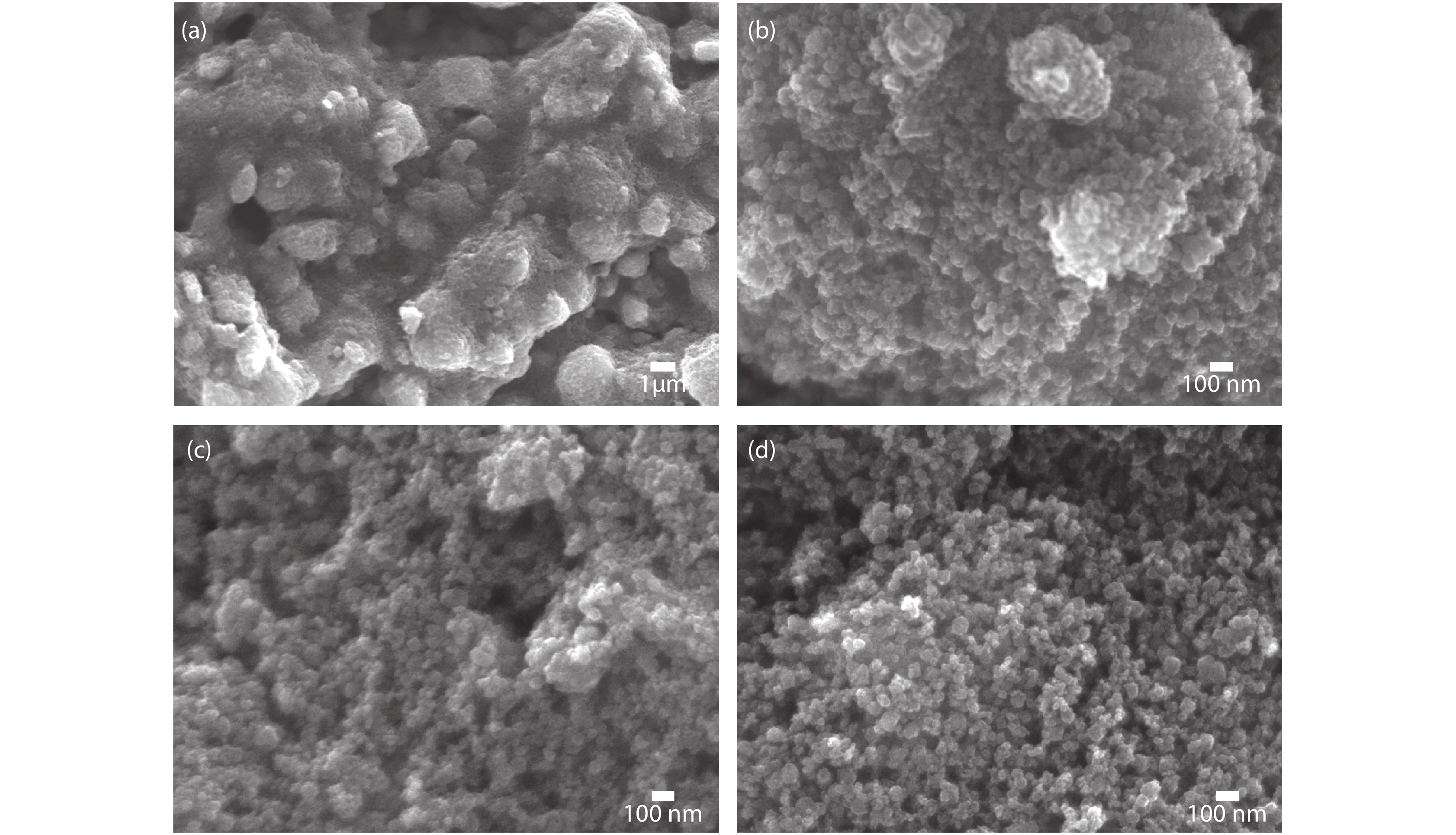
    Fig. 1. Surface morphology of pristine TiO2 at the magnifications of (a) 1000× and (b) 40 000× showing macroscopic clusters and agglomerated particles respectively, (c, d) WO3 coated TiO2 nanoparticles layer showing randomly distributed TiO2 nanoparticles and the porous nature.
    (Color online) (a–c) High resolution XPS scans showing Ti 2p, W 4f and O 1s peaks from the WO3 coated TiO2 sample. (d) XRD pattern obtained from the same sample.
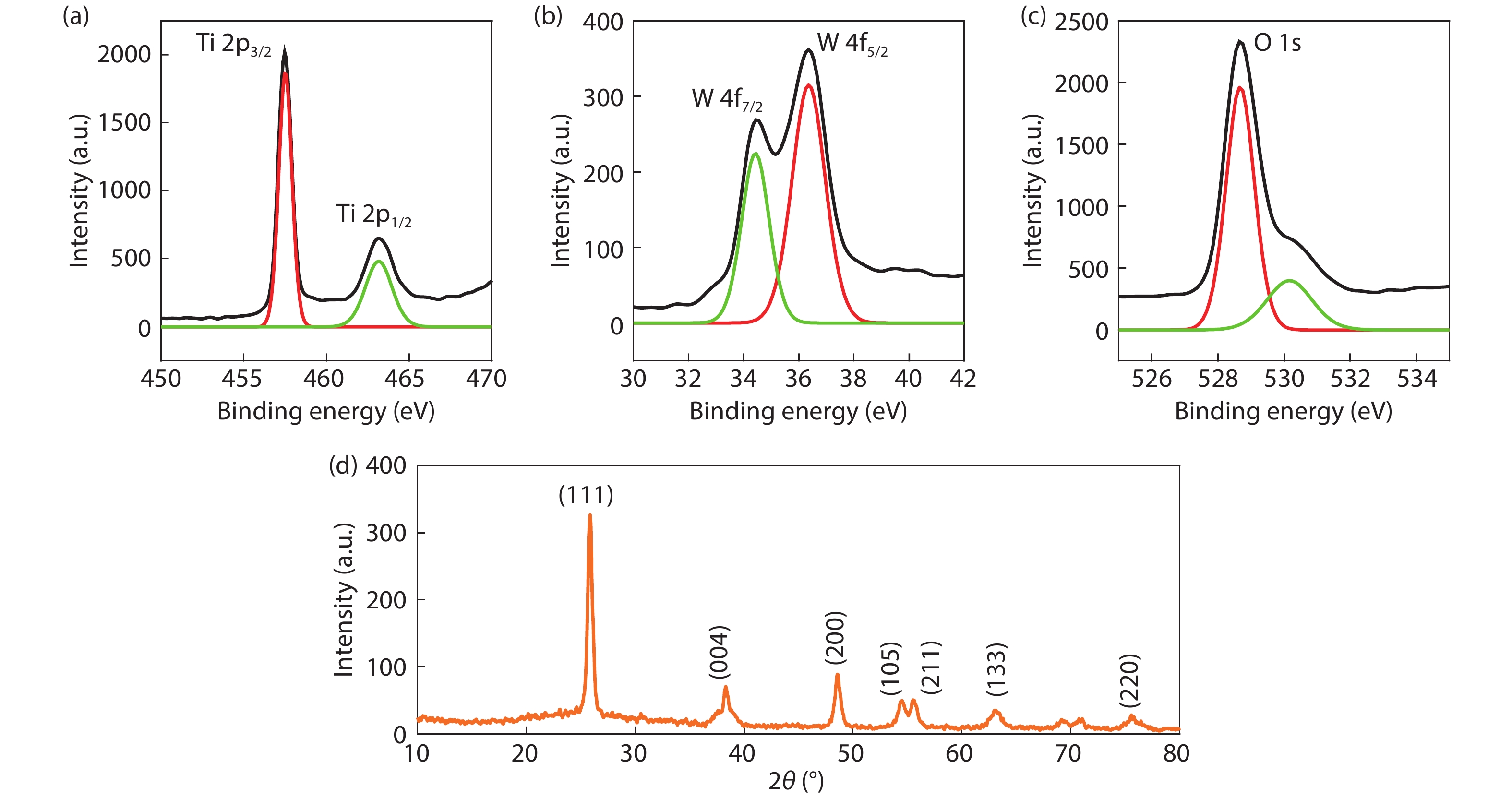
    Fig. 2. (Color online) (a–c) High resolution XPS scans showing Ti 2p, W 4f and O 1s peaks from the WO3 coated TiO2 sample. (d) XRD pattern obtained from the same sample.
    (Color online) Digital photographic images of (a) TiO2 nanoparticle layer coated on FTO covered glass substrates showing the deposition of WO3 surface passivation layer with different thickness values. (b) Photographs of the samples after N719 dye coating confirming the WO3 did not affect the loading much. (c) UV–visible absorption spectra of the samples.
    Fig. 3. (Color online) Digital photographic images of (a) TiO2 nanoparticle layer coated on FTO covered glass substrates showing the deposition of WO3 surface passivation layer with different thickness values. (b) Photographs of the samples after N719 dye coating confirming the WO3 did not affect the loading much. (c) UV–visible absorption spectra of the samples.
    (Color online) (a) J–V characteristics of the DSSC with and without WO3 passivation on TiO2. (b) Comparison of PMAX of DSSCs, dark current characteristics of DSSCs in (c) linear and (d)semi-log scale showing the saturation current values.
    Fig. 4. (Color online) (a) JV characteristics of the DSSC with and without WO3 passivation on TiO2. (b) Comparison of PMAX of DSSCs, dark current characteristics of DSSCs in (c) linear and (d)semi-log scale showing the saturation current values.
    (Color online) Schematic illustration of (a) FTO/TiO2/dye/electrolyte and (b) FTO/TiO2/WO3/Dye/electrolyte interfaces in DSSCs showing electron–hole transport and recombination mediated by defects in TiO2.
    Fig. 5. (Color online) Schematic illustration of (a) FTO/TiO2/dye/electrolyte and (b) FTO/TiO2/WO3/Dye/electrolyte interfaces in DSSCs showing electron–hole transport and recombination mediated by defects in TiO2.
    DSSCsWO3 coating duration (min) VOC (mV) JSC (mA/ cm2) FF (%)η(%) SD in η
    Pristine TiO274509.359.04.10.05
    15 nm WO3 on TiO2773211.850.84.30.06
    22 nm WO3 on TiO21071211.157.24.50.10
    30 nm WO3 on TiO21572010.053.13.80.09
    Table 1. Photovoltaic parameters of the DSSCs measured under AM1.5 illumination level.
    Arya Babu, Arya Vasanth, Shantikumar Nair, Mariyappan Shanmugam. WO3 passivation layer-coated nanostructured TiO2: An efficient defect engineered photoelectrode for dye sensitized solar cell[J]. Journal of Semiconductors, 2021, 42(5): 052701
    Download Citation