
Arya Babu, Arya Vasanth, Shantikumar Nair, Mariyappan Shanmugam. WO3 passivation layer-coated nanostructured TiO2: An efficient defect engineered photoelectrode for dye sensitized solar cell[J]. Journal of Semiconductors, 2021, 42(5): 052701
- Journal of Semiconductors
- Vol. 42, Issue 5, 052701 (2021)
Abstract
1. Introduction
The most important technological arrival of nanotechnology has endorsed multifarious nanostructured functional materials for energy conversion applications[
A variety of metal oxides and dielectrics were used in DSSCs to control the recombination at TiO2/dye/electrolyte interfaces[
The present work identified tungsten oxide (WO3) as a possible wide bandgap material which can be used for effective surface passivation on TiO2 to modify the surface to achieve better control over defects. Results showed the possibility of improving DSSC performance by coating WO3 via RF-sputtering on TiO2 in which defects are most dominating in terms of interfacial recombination.
2. Experimental section
Commercially available fluorine-doped tin oxide (FTO) glass substrates were used for DSSC fabrication process. The FTO-coated glass substrates were cleaned by sonicating them in soap solution for 15 min, then in DI water and finally with ethanol for 15 min to remove all sort of contaminations. The cleaned FTO-coated glass substrates were kept in an oven for drying at 72 ˚C. Colloidal TiO2 paste was prepared by mixing the required amount of TiO2 powder (Sigma Aldrich, 99.9% purity) and polyethylene glycolate (PEG). Both were mixed and ground thoroughly using a mortar and pestle until a required form of colloidal paste was obtained. TiO2 colloidal paste was doctor-bladed onto FTO-coated glass substrates using adhesive tape as a shadow-mask, which were removed after making the TiO2 films. Colloidal TiO2 films coating the FTO samples were then annealed at 450 ˚C for 3 h with a ramp rate of 3 ˚C per minute.
WO3 thin film was coated on TiO2 nanoparticle films using the RF sputtering technique. Samples were fixed on the substrate holder using temperature-sustainable, vacuum-compatible Kapton tape. They were placed in the RF-sputter chamber in which tungsten was used as target with oxygen as a bombarding process gas. The oxygen gas flow rate was maintained at 70 sccm with a FR-power of 25 W. To assess the effect of thickness of WO3 surface passivation on TiO2, the present study varied the thickness values of WO3 to 15, 22, and 30 nm on TiO2. This thickness variation was achieved by varying the duration of WO3 coating on TiO2 for 7, 10, and 15 min. The WO3-coated TiO2 nanoparticle layer on FTO was removed from the RF-sputter chamber and annealed at 120 ˚C.
In the present work, two categories of DSSCs were fabricated using (i) pristine TiO2 and (ii) WO3-coated TiO2 to validate the effect of WO3 passivation on TiO2 nanoparticle layer in DSSC performance. Ruthenium-based N719 dye was prepared using a mixture of 50 mL of tert-butyl alcohol and 50 mL of acetonitrile. Then, 0.5 mM of N719 dye (59.43 mg for 100 mL) was added and stirred for 30 min to make the required homogeneous N719 dye. The pristine TiO2 and WO3-coated TiO2 samples prepared on FTO-coated glass substrates were immersed in dye solution to sensitize. DSSCs were fabricated using N719-adsorbed pristine TiO2 and WO3-coated TiO2 as photo-anodes to compare the effect of WO3 passivation. Hole-transporting iodide/tri-iodide was used as an electrolyte along with a platinum counter electrode for the DSSCs. The only difference between the two categories of DSSCs was the WO3 passivation on the TiO2 nanoparticle layer.
Surface morphology of the pristine and WO3-coated TiO2 samples were characterized using a JSN 7610S Plus JEOL-JSM-6490-LA scanning electron microscope (FESEM). X-ray photoelectron spectroscopy (XPS) used a Kratos Analytical unit. X-ray diffraction (XRD) patterns of the WO3 coated samples were obtained using PANalytical X’Pert PRO X-Ray Diffractometer. UV–visible optical spectra of the samples were obtained in a Perkin Elmer Lambda-750 UV–visible spectrometer. The fabricated DSSCs were characterized under 1-Sun illumination (AM 1.5 G) in a Newport Oriel Class A solar simulator to measure required J–V characteristics using a Keithley-2420 digital source meter.
3. Results and discussion
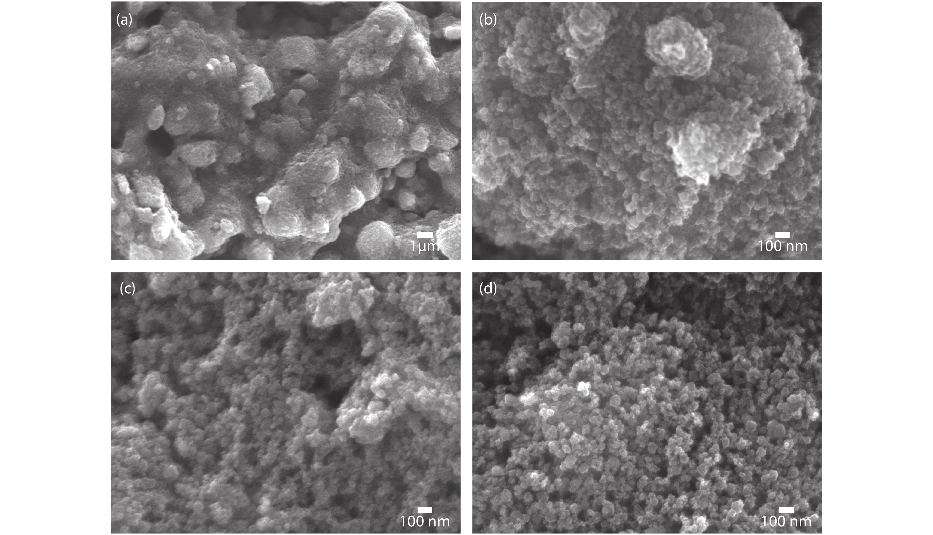
Figs. 1(a) and 1(b) show surface morphology of the TiO2 nanoparticle layer coated on the FTO substrate for DSSC fabrication. Macroscopic clustered TiO2 was observed at the low (1000×) magnification in Fig. 1(a), and a further magnified image exhibited smaller size TiO2 particles agglomerated on the macroscopic clusters as shown in Fig. 1(b) which was obtained at the magnification of 40 000×. While the lower magnified image exhibited a macroscopic cluster film, the higher one showed the nanoparticles agglomerated as clusters. Figs. 1(c) and 1(d) were obtained from the TiO2 nanoparticle layer after coating the WO3 passivation layer at 15 and 30 nm, respectively. It is evident that the coating of thin WO3 on the TiO2 nanoparticle layer did not change the morphology significantly in terms of surface morphology. The WO3 coating was performed by RF-sputtering, which is a gas-phase plasma assisted physical vapor deposition process to achieve uniform coating of functional material. The surface morphology images shown in Figs. 1(c) and 1(d) clearly addressed the pristine nature of the TiO2 nanoparticle layer was not modified as the RF-sputtering process uniformly covered the TiO2 nanoparticles and the coating did not block the porosity of the TiO2, as can be seen in Figs. 1(a) and 1(b). In general, the surface passivation coating is applied on nanostructured functional materials in which defects are playing a dominated role on charge transport characteristics and deteriorates the performance of the resulting solar cells. Thus, it is essential to coat the surface passivation layer but if it is too thick or not uniform then the surface passivation layer itself might block the charge transport and thus recombination would dominate. In the present study, the surface morphology images prove that WO3 did not affect TiO2 morphology as it was thin enough and uniform.
![]()
Figure 1.Surface morphology of pristine TiO2 at the magnifications of (a) 1000× and (b) 40 000× showing macroscopic clusters and agglomerated particles respectively, (c, d) WO3 coated TiO2 nanoparticles layer showing randomly distributed TiO2 nanoparticles and the porous nature.
Fig. 2 shows results from XPS and XRD studies performed on the WO3-coated TiO2 nanoparticle layer. Fig. 2(a) shows a high-resolution XPS scan obtained from the sample showing Ti 2p peaks. Specifically, Ti 2p3/2 and Ti 2p1/2 were 457.4 and 463.1 eV respectively, showing the spin-orbital splitting of photoelectrons. The binding energy difference between two peaks was 5.7 eV. Fig. 2(b) shows a high-resolution XPS scan of tungsten (W) which belongs to the WO3 passivation layer on the TiO2 nanoparticle layer. The spin-orbital splitting of photoelectrons exhibited W 4f7/2 and W 4f5/2 at the binding energy values of 34.4 and 36.3 eV respectively. The energy difference between the two peaks was observed to be 1.9 eV. The high-resolution XPS scan showing O 1s spectrum obtained from the sample is shown in Fig. 2(c). The peak occurred at 528.7 eV. All these characteristic peaks, identified with respect to their binding energy values, confirmed the WO3 coating on the TiO2 nanoparticle layer. Fig. 2(d) shows XRD pattern of the WO3-coated TiO2 nanoparticle layer. The XRD peak appeared at 2θ of 25.8° represents (101) which corresponds to the anatase TiO2 phase and this was confirmed from JCPDS-84-1286. The TiO2 is considered to be phase pure as it did not show the rutile phase at 2θ value of 27.36°. Further the XRD peaks at 2θ values of 38.3° (004), 48.5° (200) and 55.6° (211) also assert the TiO2 nanoparticle layer. The indices (105), (133) and (220) at 2θ values of 54.4°, 63.1°, 75.5° represent the WO3 thin film coating on the TiO2 nanoparticle layer. Thus, the XRD pattern obtained from the WO3 passivation thin film-coated TiO2 nanoparticle layer also confirmed both the functional materials with respective to their characteristic peaks.
![]()
Figure 2.(Color online) (a–c) High resolution XPS scans showing Ti 2p, W 4f and O 1s peaks from the WO3 coated TiO2 sample. (d) XRD pattern obtained from the same sample.
Fig. 3(a) shows photographs of the pristine TiO2 nanoparticle layer along with 15, 22, 30 nm WO3-coated TiO2. It was very obvious that WO3 passivation was thin enough, which did not change the TiO2 much in terms of the color. However, it was very clear from the picture that WO3 was coated on the surface of the TiO2 nanoparticle film. In this study, WO3 was coated on TiO2 to modify/suppress the defects which are actively participating in the charge transport process in DSSCs. Thus, it was a genuine expectation that WO3 should not affect the dye adsorption on the surface of TiO2. The photograph shown in Fig. 3(b) shows the pristine TiO2 nanoparticle layer along with 15, 22, and 30 nm WO3-coated TiO2 after the dye loading process. It provided evidence that coating of WO3 on the TiO2 nanoparticle layer did not affect the dye loading significantly. In general, a surface passivation layer is expected to control the defects in semiconductors to improve the charge transport characteristics to yield high performance photovoltaic devices. If the dye loading into the TiO2 nanoparticle layer is impeded by WO3, then exciton generation will be reduced significantly which, in turn, would result in lower photo-current and overall performance. Fig. 3(c) shows UV–visible optical absorption spectroscopic measurements performed on the pristine TiO2 nanoparticle layer in comparison with TiO2 samples coated with the 15, 22, and 30 nm WO3 surface passivation layer. As shown in the Fig. 3(c), the pristine and WO3-coated TiO2 did not show any significant absorption in the spectral window of 400–800 nm in which a major portion of visible energy photons are available. Thus, passivating TiO2 by WO3 will not impede visible spectral photons to reach dye molecules to generate excitons. Thus, WO3 coating on TiO2 can be categorized as an advantage for DSSC operation in terms of defect passivation but has no disadvantage in terms of absorption loss due to the optimum band structure characteristics. In DSSCs, incident photons enter through a transparent electrode, FTO, and travel through the TiO2 nanoparticle layer to reach organic dye to generate excitons. Passivation layers are coated on TiO2 in DSSCs to control defects. If the passivation layer scatters or disperses photons between TiO2 and dye, it will lead to major optical loss which would affect the photo-current generation. Thus, it is important to confirm the passivation layer does not interact with incident photons in the visible spectral range. Further, UV–visible spectra of WO3-coated TiO2 samples exhibited that absorption at the high energy spectral region was significantly suppressed after WO3 coating. WO3 exhibits an optical bandgap in the range of 2.6–3 eV. When pristine TiO2 showed absorption in the high energy range, WO3 coating suppressed the exciton generation at this specific range due to the heterostructure alignment in the band-structure[
![]()
Figure 3.(Color online) Digital photographic images of (a) TiO2 nanoparticle layer coated on FTO covered glass substrates showing the deposition of WO3 surface passivation layer with different thickness values. (b) Photographs of the samples after N719 dye coating confirming the WO3 did not affect the loading much. (c) UV–visible absorption spectra of the samples.
Fig. 4(a) shows illuminated J–V characteristics of the DSSCs which used pristine TiO2 as a photo-anode along with the WO3 passivation layer-coated TiO2. The illuminated J–V characteristics of the DSSCs showed that coating of WO3 on the TiO2 nanoparticle played a significant role in terms of all photovoltaic parameters including open circuit voltage (VOC), short circuit current density (JSC), fill factor (FF) and efficiency (η). All the key photovoltaic parameters measured under AM 1.5 illumination are listed in Table 1 along with standard deviation in η. The reference DSSC, which used a pristine TiO2-based photo-anode (no WO3 coating), resulted in VOC, JSC, FF and η of 745 mV, 9.3 mA/cm2, 59.0%, and 4.1% respectively. The DSSC, which used 22 nm coating of WO3 on TiO2 as a photo-anode, resulted in VOC, JSC, FF and η of 712 mV, 11.1 mA/cm2, 57.2%, and 4.5%, respectively. This is approximately 10% enhancement in η due to the increment in JSC. As can be seen in Table 1, further increment in the duration of WO3 coating on TiO2 affected photovoltaic parameters significantly. It can be directly attributed to the reduction in JSC by creating a thicker energy barrier between the TiO2 and dye where the charge carrier injection occurred. It is well known that if the energy barrier thickness increases, then tunneling probability would decrease. Thus, an optimum thickness of the passivation layer is required to passivate the defects. In the present study, it was found that 10 min WO3 coating on TiO2 performed better than other DSSCs.
![]()
Figure 4.(Color online) (a)
Fig. 4(b) shows power density–voltage characteristics of the reference DSSCs along with DSSCs used WO3 passivation showing the maximum power point (PMAX) values. It was noticed that DSSC used 10 min of WO3 passivation on TiO2 resulted in 4.5 mW/cm2 while the reference DSSC exhibited 4 mW/cm2. This is one of the parameters along with the increment in JSC improved the ~10% enhancement in η for the DSSC with 22 nm WO3 passivation on TiO2. The DSSC with 15 min of WO3 passivation showed 3.8 mW/cm2. It clearly indicated that increasing thickness of WO3 affected the PMAX and thus the detrimental effect on photovoltaic performance. Fig. 4(c) shows dark current–voltage characteristics of the DSSCs with a semi-log plot of the same in the higher applied range of 0.7 to 1 V. It is possible to assess the electronic quality of interfaces in DSSCs through dark saturation current (IO) which can be obtained from the general ID = IOexp(qV/kT–1), where ID and IO are current density and saturation current respectively under dark conditions. The parameters in equation q, V, k and T are electronic charge, applied bias to the DSSCs, Boltzmann constant and temperature at which the DSSCs work respectively. It is well known that DSSCs with good quality interfaces exhibit higher IO values at higher applied bias regions, lower IO values at lower and medium forward bias regions. Increasing IO in the low and medium forward bias regions can directly be attributed to the defect dominated charge transport. Thus, the parameter (IO) needs to be suppressed to obtain a DSSC with improved photovoltaic performance. Inset in Fig. 4(c) clearly showed the DSSC with 10 min WO3 coating resulted in higher IO value compared with other DSSCs. Fig. 4(d) shows semi-log plots of dark current characteristics of the reference DSSC along with DSSC used WO3 passivation. We have chosen the applied bias region close to 0.3 V to consider the IO values for the DSSCs. It is evident that DSSC with 10 min of WO3 passivation on TiO2 exhibited 1 × 10⁻⁷ A, which is 20 times lower than the IO values showed by reference DSSC which was 2 × 10⁻⁶ A. In this calculation, 0.3 V applied bias has been considered to extract the IO values for all DSSCs for the reason that a linear dark current increment was observed in the semi-log plot as shown in Fig. 4(d). If the dark current is highly linear in the log-scale, it is a perfect exponential diode characteristic feature. Thus, the applied bias of 0.3 V has been used to extract IO values.
Figs. 5(a) and 5(b) show the energy level diagram representing FTO/TiO2/dye/electrolyte and FTO/TiO2/WO3/Dye/electrolyte interfaces respectively. The only difference between the two categories of DSSCs examined in the present work was WO3 passivation on TiO2. Thus, the variation in photovoltaic performance is directly attributed to the ability of WO3 to passivate defects in TiO2. Photo-generated electrons in the lowest unoccupied molecular orbital (LUMO) of the dye need to be injected into the conduction band edge of TiO2 (EC) in which they are all transported to reach the FTO electrode by diffusion as represented by process (1). Meanwhile, the holes from the highest occupied molecular orbital (HOMO) of the dye will be regenerated by the electrolyte as shown in process (2). These two categories are electron and hole transport, which eventually contribute to photo-current in DSSCs. However, the photo-electrons in the bulk of TiO2 nanoparticle layer can be trapped by defects present in the bandgap of TiO2 as illustrated by process (3). If the trap states, which are close to the trapped electron, can trap a hole from the HOMO of the dye as shown in process (4), then electron-hole recombination will occur at the bandgap of TiO2 mediated by defects. Fig. 5(b) shows the possible changes that can occur at the electron–hole transport and recombination kinetics after coating the WO3 surface passivation layer on TiO2. The photo-generated electron injection from the LUMO of the dye will be injected through the WO3 surface passivation layer by tunneling as the thickness is facilitating such a transport process. Photo-generated electrons in the TiO2 further can be trapped by defects but the probability of hole trapping, process (4), is rather difficult as the WO3 will not allow the trap states in TiO2 to interact with holes at the HOMO of the dye. Thus, hole trapping will not occur at the TiO2/dye interface after coating the passivation layer. The photo-generated electron will not be lost without having a hole in the bulk vicinity of TiO2. The probability of recombination loss is expected to be suppressed by coating a thin WO3 film on TiO2. This situation will lead to improved DSSC performance.
![]()
Figure 5.(Color online) Schematic illustration of (a) FTO/TiO2/dye/electrolyte and (b) FTO/TiO2/WO3/Dye/electrolyte interfaces in DSSCs showing electron–hole transport and recombination mediated by defects in TiO2.
4. Conclusion
A dominant recombination pathway at the TiO2/dye interface was significantly suppressed by passivating the TiO2 surface using RF-sputtered WO3 film. RF-sputtering is a versatile technique to coat WO3 surface passivation on the TiO2 nanoparticle layer without blocking the porosity. DSSC with WO3 passivation exhibited ~10% enhancement in performance. Results from DSSCs confirmed that there is an optimum thickness of WO3, at which the electron-hole transport was facilitated while the recombination probability was reduced.
Acknowledgements
We thank the Amrita Centre for Nanosciences for providing us with the PVD cluster equipment to coat various functional thin films for the energy conversion technology development.
References
[1] V Mlinar. Engineered nanomaterials for solar energy conversion. Nanotechnology, 24, 042001(2013).
[2] S Kumar, M Nehra, A Deep et al. Quantum-sized nanomaterials for solar cell applications. Renew Sustain Energy Rev, 73, 821(2017).
[3] H Sun, J Deng, L B Qiu et al. Recent progress in solar cells based on one-dimensional nanomaterials. Energy Environ Sci, 8, 1139(2015).
[4] L J Brennan, M T Byrne, M Bari et al. Carbon nanomaterials for dye-sensitized solar cell applications: A bright future. Adv Energy Mater, 1, 472(2011).
[5] N L Yang, J Zhai, D Wang et al. Two-dimensional graphene bridges enhanced photoinduced charge transport in dye-sensitized solar cells. ACS Nano, 4, 887(2010).
[6] R Yu, Q F Lin, S F Leung et al. Nanomaterials and nanostructures for efficient light absorption and photovoltaics. Nano Energy, 1, 57(2012).
[7] Y Hu, H Wang, B Hu. Thinnest two-dimensional nanomaterial— graphene for solar energy. ChemSusChem, 3, 782(2010).
[8] W Li, A Elzatahry, D Aldhayan et al. Core-shell structured titanium dioxide nanomaterials for solar energy utilization. Chem Soc Rev, 47, 8203(2018).
[9] S Su, W H Wu, J M Gao et al. Nanomaterials-based sensors for applications in environmental monitoring. J Mater Chem, 22, 18101(2012).
[10] Y M Sun, N Liu, Y Cui. Promises and challenges of nanomaterials for lithium-based rechargeable batteries. Nat Energy, 1, 16071(2016).
[11] M Gao, J C Yao, C Yan et al. Novel composite nanomaterials with superior thermal and pressure stability for potential LED applications. J Alloy Compd, 734, 282(2018).
[12] G Ramakrishna, A K Singh, D K Palit et al. Dynamics of interfacial electron transfer from photoexcited quinizarin (Qz) into the conduction band of TiO2 and surface states of ZrO2 nanoparticles. J Phys Chem B, 108, 4775(2004).
[13] I Hanzu, T Djenizian, P Knauth. Electrical and point defect properties of TiO2 nanotubes fabricated by electrochemical anodization. J Phys Chem C, 115, 5989(2011).
[14] F Nasirpouri, N S Peighambardoust, A Samardak et al. Structural defect-induced bandgap narrowing in dopant-free anodic TiO2 nanotubes. ChemElectroChem, 4, 1227(2017).
[15] H Menon, G Gopakumar, V Sankaranarayanan Nair et al. 2D-layered MoS2-incorporated TiO2-nanofiber- based dye-sensitized solar cells. ChemistrySelect, 3, 5801(2018).
[16] A Goban, K S Choi, D J Alton et al. Demonstration of a state-insensitive, compensated nanofiber trap. Phys Rev Lett, 109, 033603(2012).
[17] H Zhu, M M Zhao, J K Zhou et al. Surface states as electron transfer pathway enhanced charge separation in TiO2 nanotube water splitting photoanodes. Appl Catal B, 234, 100(2018).
[18] M Sachs, E Pastor, A Kafizas et al. Evaluation of surface state mediated charge recombination in anatase and rutile TiO2. J Phys Chem Lett, 7, 3742(2016).
[19] J W Zheng, L E Mo, W C Chen et al. An investigation of surface states energy distribution and band edge shifts in solar cells based on TiO2 submicrospheres and nanoparticles. Electrochimica Acta, 232, 38(2017).
[20] T Sidorova. A model of electron tunneling to the surface states in TiO2 with application to photocatalysis. Int J Nanosci, 18, 1940034(2019).
[21] C Fàbrega, D Monllor-Satoca, S Ampudia et al. Tuning the fermi level and the kinetics of surface states of TiO2 nanorods by means of ammonia treatments. J Phys Chem C, 117, 20517(2013).
[22] R Huber, S Spörlein, J E Moser et al. The role of surface states in the ultrafast photoinduced electron transfer from sensitizing dye molecules to semiconductor colloids. J Phys Chem B, 104, 8995(2000).
[23] M Antuch, P Millet, A de Iwase et al. The role of surface states during photocurrent switching: Intensity modulated photocurrent spectroscopy analysis of BiVO4 photoelectrodes. Appl Catal B, 237, 401(2018).
[24] M K Hossain, A A Mortuza, S K Sen et al. A comparative study on the influence of pure anatase and Degussa-P25 TiO2 nanomaterials on the structural and optical properties of dye sensitized solar cell (DSSC) photoanode. Optik, 171, 507(2018).
[25] C K Kim, J M Ji, H Zhou et al. Tellurium-doped, mesoporous carbon nanomaterials as transparent metal-free counter electrodes for high-performance bifacial dye-sensitized solar cells. Nanomaterials, 10, E29(2019).
[26] S Mehra, S Bishnoi, A Jaiswal et al. A review on spectral converting nanomaterials as a photoanode layer in dye-sensitized solar cells with implementation in energy storage devices. Energy Storage, 2, e120(2020).
[27] K K Tehare, S T Navale, F J Stadler et al. Enhanced DSSCs performance of TiO2 nanostructure by surface passivation layers. Mater Res Bull, 99, 491(2018).
[28] G Gopakumar, A Ashok, S N Vijayaraghavan et al. MoO3 surface passivation on TiO2: An efficient approach to minimize loss in fill factor and maximum power of dye sensitized solar cell. Appl Surf Sci, 447, 554(2018).
[29] K E Roelofs, T P Brennan, J C Dominguez et al. Effect of Al2O3 recombination barrier layers deposited by atomic layer deposition in solid-state CdS quantum dot-sensitized solar cells. J Phys Chem C, 117, 5584(2013).
[30] A R Pascoe, L Bourgeois, N W Duffy et al. Surface state recombination and passivation in nanocrystalline TiO2 dye-sensitized solar cells. J Phys Chem C, 117, 25118(2013).
[31] C Prasittichai, J T Hupp. Surface modification of SnO2 photoelectrodes in dye-sensitized solar cells: Significant improvements in photovoltage via Al2O3 atomic layer deposition. J Phys Chem Lett, 1, 1611(2010).
[32] E Palomares, J N Clifford, S A Haque et al. Slow charge recombination in dye-sensitised solar cells (DSSC) using Al2O3 coated nanoporous TiO2 films. Chem Commun (Camb), 14, 1464(2002).
[33] Y J Wang, W K Bai, S L Han et al. Promoted photoelectrocatalytic hydrogen production performance of TiO2 nanowire arrays by Al2O3 surface passivation layer. Curr Catal, 6, 50(2017).
[34] J A Jeong, H K Kim. Thickness effect of RF sputtered TiO2 passivating layer on the performance of dye-sensitized solar cells. Sol Energy Mater Sol Cells, 95, 344(2011).
[35] M Shanmugam, R Jacobs-Gedrim, C Durcan et al. 2D layered insulator hexagonal boron nitride enabled surface passivation in dye sensitized solar cells. Nanoscale, 5, 11275(2013).
[36] X J Yang, L Zhao, K Lv et al. Enhanced efficiency for dye-sensitized solar cells with ZrO2 as a barrier layer on TiO2 nanofibers. Appl Surf Sci, 469, 821(2019).
[37] J A van Delft, D Garcia-Alonso, W M Kessels. Atomic layer deposition for photovoltaics: Applications and prospects for solar cell manufacturing. Semicond Sci Technol, 27, 074002(2012).
[38] A Vasanth, N S Powar, D Krishnan et al. Electrophoretic graphene oxide surface passivation on titanium dioxide for dye sensitized solar cell application. J Sci: Adv Mater Devices, 5, 316(2020).
[39] C J Flynn, S M McCullough, E Oh et al. Site-selective passivation of defects in NiO solar photocathodes by targeted atomic deposition. ACS Appl Mater Interfaces, 8, 4754(2016).
[40] H Sun, H Kurotaki, K Kanomata et al. ZnO/TiO2 core-shell photoelectrodes for dye-sensitized solar cells by screen printing and room temperature ALD. Microsyst Technol, 24, 647(2018).
[41] J R Bakke, K L Pickrahn, T P Brennan et al. Nanoengineering and interfacial engineering of photovoltaics by atomic layer deposition. Nanoscale, 3, 3482(2011).
[42] L P Li, S K Chen, C Xu et al. Comparing electron recombination via interfacial modifications in dye-sensitized solar cells. ACS Appl Mater Interfaces, 6, 20978(2014).
[43] C B Fei, J J Tian, Y J Wang et al. Improved charge generation and collection in dye-sensitized solar cells with modified photoanode surface. Nano Energy, 10, 353(2014).
[44] S A Kim, M A Abbas, L Lee et al. Control of morphology and defect density in zinc oxide for improved dye-sensitized solar cells. Phys Chem Chem Phys, 18, 30475(2016).
[45] G Arthi, J Archana, M Navaneethan et al. Hydrothermal growth of ligand-passivated high-surface-area TiO2 nanoparticles and dye-sensitized solar cell characteristics. Scr Mater, 68, 396(2013).
[46] S W Rhee, H W Choi. Influence of RF magnetron sputtering condition on the ZnO passivating layer for dye-sensitized solar cells. Trans Electr Electron Mater, 14, 86(2013).
[47] S Y Lee, S H Kim. Deposition of TiO2 passivation layer by plasma enhanced chemical vapor deposition between the transparent conducting oxide and mesoporous TiO2 electrode in dye sensitized solar cells. Jpn J Appl Phys, 51, 10NE19(2012).
[48] C Y Neo, J Y Ouyang. Precise modification of the interface between titanium dioxide and electrolyte of dye-sensitized solar cells with oxides deposited by thermal evaporation of metals and subsequent oxidation. J Power Sources, 196, 10538(2011).
[49] Y S Jin, H W Choi. Properties of dye-sensitized solar cells with TiO2 passivating layers prepared by electron-beam evaporation. J Nanosci Nanotechnol, 12, 662(2012).
[50] N Tétreault, L P Heiniger, M Stefik et al. Atomic layer deposition for novel dye-sensitized solar cells. ECS Trans, 41, 303(2019).
[51] M Zafar, B Kim, D H Kim. Improvement in performance of inverted polymer solar cells by interface engineering of ALD ZnS on ZnO electron buffer layer. Appl Surf Sci, 481, 1442(2019).
[52] T Cossuet, E Appert, O Chaix-Pluchery et al. Epitaxial TiO2 shell grown by atomic layer deposition on ZnO nanowires using a double-step process and its beneficial passivation effect. J Phys Chem C, 124, 13447(2020).
[53] D H Kim, M D Losego, Q Peng et al. Atomic layer deposition for sensitized solar cells: Recent progress and prospects. Adv Mater Interfaces, 3, 1600354(2016).
[54]
[55] L F Paula, M Hofer, V P B Lacerda et al. Unraveling the photocatalytic properties of TiO2/WO3 mixed oxides. Photochem Photobiol Sci, 18, 2469(2019).

Set citation alerts for the article
Please enter your email address
© Copyright 2018-2021 | Chinese Laser Press. All Rights Reserved 沪ICP备15018463号-20