
Xuefen Cai, Peng Zhang, Su-Huai Wei. Revisit of the band gaps of rutile SnO2 and TiO2: a first-principles study[J]. Journal of Semiconductors, 2019, 40(9): 092101
- Journal of Semiconductors
- Vol. 40, Issue 9, 092101 (2019)
![(Color online) Band gaps and band alignments between rutile SnO2 and TiO2. In (a) the band gaps of SnO2 is taken from Ref. [15] and the CB band alignment is taken from Ref. [19], while in (b) both of them are calculated in this work. The band gap of TiO2 is always set to its experimental value (taken from Ref. [20]).](/richHtml/jos/2019/40/9/092101/img_1.jpg)
Fig. 1. (Color online) Band gaps and band alignments between rutile SnO2 and TiO2. In (a) the band gaps of SnO2 is taken from Ref. [15 ] and the CB band alignment is taken from Ref. [19 ], while in (b) both of them are calculated in this work. The band gap of TiO2 is always set to its experimental value (taken from Ref. [20 ]).
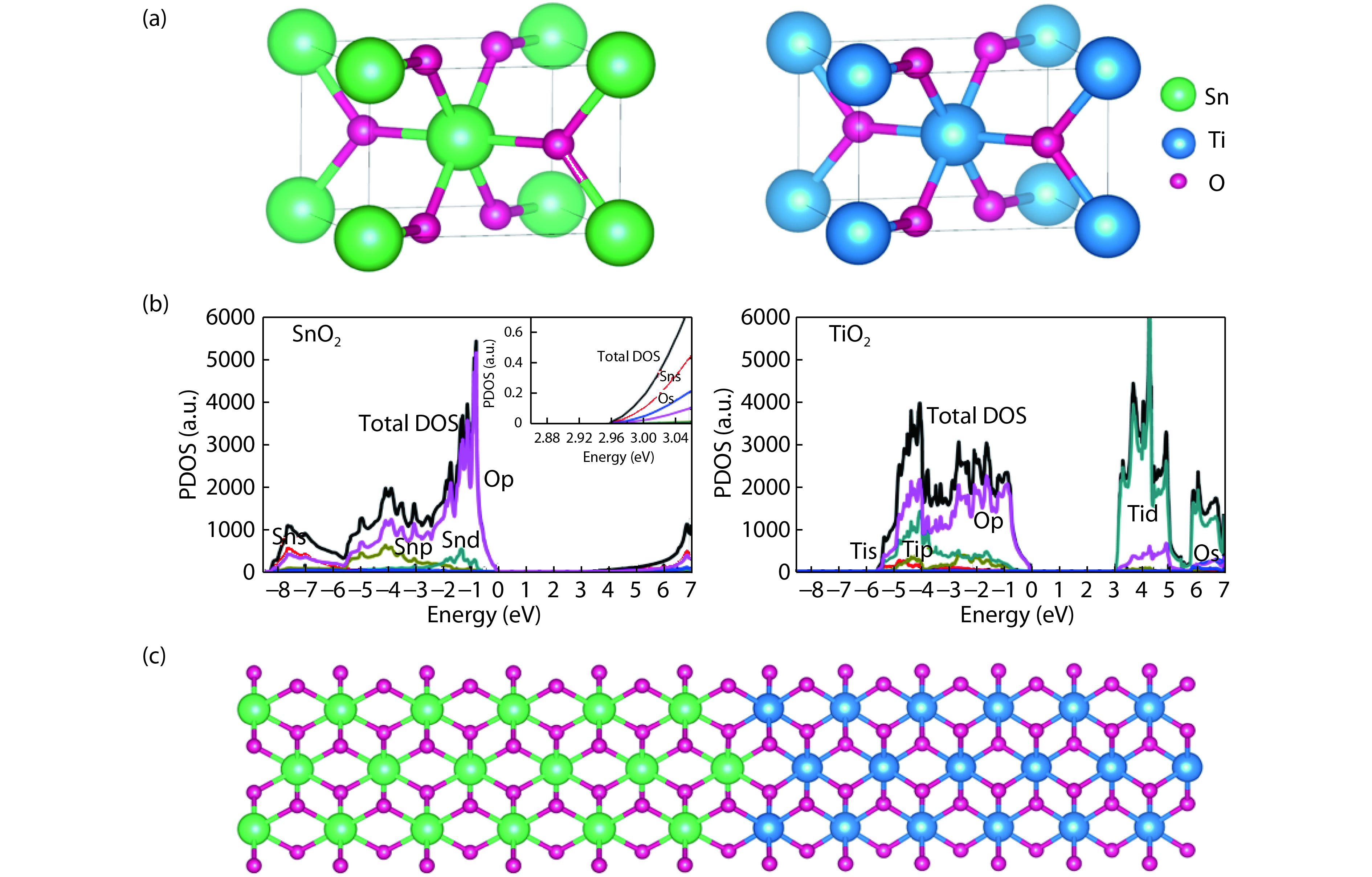
Fig. 2. (Color online) (a) Primitive unit cells and (b) calculated total and partial density of states for rutile SnO2 and TiO2. The green, blue and purple balls represent Sn, Ti and O respectively. (c) Side view of the atomic configuration for SnO2/TiO2 heterojunction (top panel).
Fig. 3. (Color online) (a) Band structure of SnO2 along two high symmetry lines M–Γ–Z. (b) Optical absorption coefficient of SnO2. The valence band maximum is set at zero. In (a), the red and green arrows represent the possible optical transitions at Γ-point and away from Γ-point, respectively.
Fig. 4. (Color online) Differences between the HSE06 + G0W0 calculated and experimentally measured band gaps
Fig. 5. (Color online) Calculated DOS of SnO2 for the valence bands below VBM level. The right-hand side shows the DOS with enlarged energy scale below the VBM at E = 0 eV.
|
Table 1. The calculated optical transition matrix elements (in arbitrary units) between the valence band states and conduction band states for rutile SnO2. Three transition paths are considered: two are at Γ-point and one is at the vicinity of Γ-point, as shown in Fig. 3 . The energy for the valance (E VB) and conduction band states (E CB) are calculated with respect to the VBM and their energy difference is ΔE = E CB – E VB.
|
Table 2. Calculated fundamental band gaps (eV) of rutile TiO2 and SnO2 using different calculation methods and functionals.
|
Table 3. The calculated fundamental band gaps by HSE06 + G0W0 method (


Set citation alerts for the article
Please enter your email address

© Copyright 2018-2021 | Chinese Laser Press. All Rights Reserved 沪ICP备15018463号-20