
Xuefen Cai, Peng Zhang, Su-Huai Wei. Revisit of the band gaps of rutile SnO2 and TiO2: a first-principles study[J]. Journal of Semiconductors, 2019, 40(9): 092101
- Journal of Semiconductors
- Vol. 40, Issue 9, 092101 (2019)
Abstract
1. Introduction
Post-transition-metal oxides, such as In2O3 and SnO2, have been extensively used as transparent conducting oxides (TCOs), a unique class of materials that combine the high electrical conductivity and optical transmission in the visible or near-infrared spectral range, which are needed in various optoelectronic devices, such as solar cells, flat-panel displays, light emitting diodes (LEDs) and transparent transistors[
In contrast to the case of In2O3, the band gap problem of SnO2 is still not fully understood, largely because of the lack of detailed experimental measurements. Analogous to bixbyite In2O3, rutile SnO2 also has the inversion symmetry and the dipole-forbidden transitions between the band edge states. As a result, one may expect different fundamental and optical gaps of SnO2 as well, which, however, has never been reported in experiments. The single-photon and two-photon absorption experiments showed an optical gap of SnO2 at ~3.60 eV, which has been widely taken as its “band gap”[
Despite the absence of direct measurements on its fundamental gap, more insight can be obtained from the recent experiments where SnO2 was employed as the electron transport layer (ETL) in both dye-sensitized and perovskite solar cells to replace the commonly used TiO2[
![]()
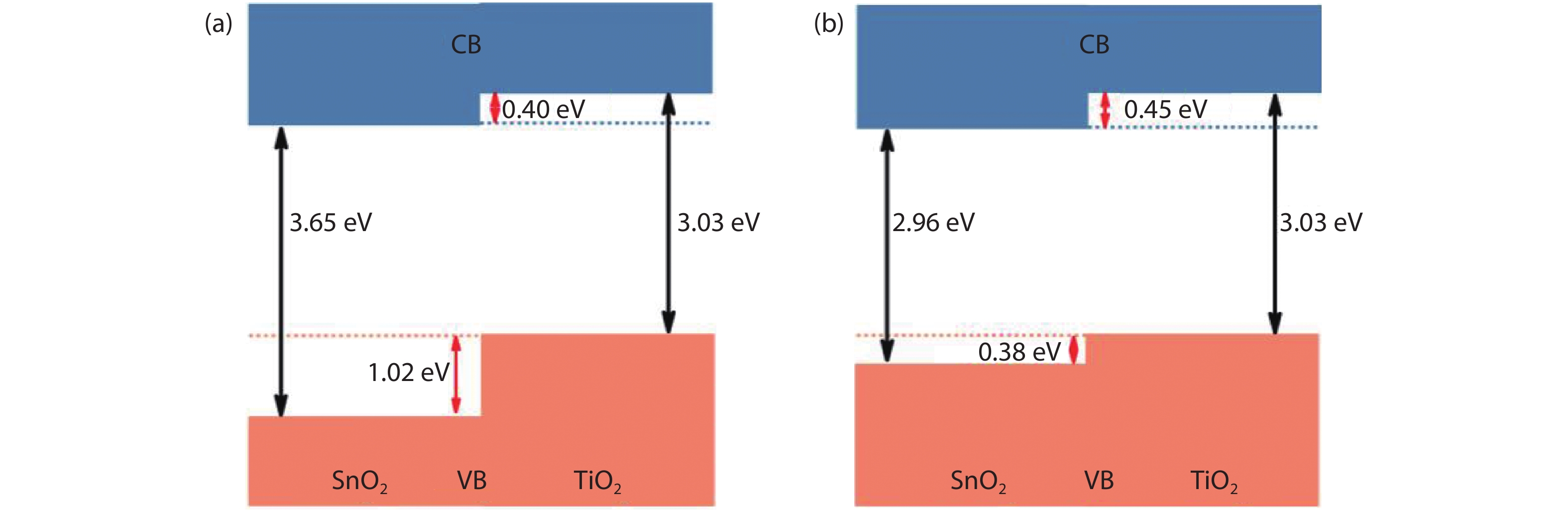
Figure 1.(Color online) Band gaps and band alignments between rutile SnO2 and TiO2. In (a) the band gaps of SnO2 is taken from Ref. [
To address this issue, in this work, we revisit the band gap problem for the rutile SnO2 by using first-principles calculations. Different-level computational methods and functionals, such as PBE, PBE + G0W0, HSE06 and HSE06 + G0W0 are employed and the results are carefully compared. We find that the HSE06 calculations yield a VB offset of 0.38 eV between SnO2 and TiO2, generally obeying the common-anion rule. The fundamental gap is calculated to be 2.96 eV, which is much smaller than the previously reported value. The conduction band (CB) offset is then found to be 0.45 eV, in good agreement with experiments[
2. Theoretical calculation
Our calculations are carried out using the projector augmented wave (PAW) method[
3. Results and discussion
Fig. 2(a) illustrates the tetragonal rutile structure for both SnO2 and TiO2 with the space group
![]()
Figure 2.(Color online) (a) Primitive unit cells and (b) calculated total and partial density of states for rutile SnO2 and TiO2. The green, blue and purple balls represent Sn, Ti and O respectively. (c) Side view of the atomic configuration for SnO2/TiO2 heterojunction (top panel).
The first two terms on the right-hand side are the core-level to VBM energy separations for pure bulk TiO2 and SnO2, respectively, and the third term
The calculated band alignment for SnO2 and TiO2 is shown in Fig. 1(b). We find that the VBM of SnO2 is 0.38 eV lower in energy than that of TiO2, which generally follows the common-anion rule. The slightly lower VBM of SnO2 can be attributed to the more polar Sn4+ ions, compared to Ti4+ ions. The calculated fundamental gaps of SnO2 and TiO2 are 2.96 and 3.15 eV, respectively, with the latter slightly larger than the experimental value of 3.03 eV[
![]()
Figure 3.(Color online) (a) Band structure of SnO2 along two high symmetry lines M–Γ–Z. (b) Optical absorption coefficient of SnO2. The valence band maximum is set at zero. In (a), the red and green arrows represent the possible optical transitions at Γ-point and away from Γ-point, respectively.
Table Infomation Is Not EnableIt should be noted that the fundamental gap of SnO2 obtained here is quite different from the values reported by the previous calculations[
One may argue that the hybrid functional and/or GW approximation may have different impacts on the fundamental gaps of SnO2 and TiO2, because of the different component of their CBM states, as shown in Fig. 1(b). To clarify this point, we consider a series of metal oxides, including ZnO, CdO, Ga2O3, In2O3 and GeO2, for which the CBM and VBM components are all similar to that of SnO2. Table 3 gives the calculated fundamental gaps by the HSE06 + G0W0 method, together with the available experimental data. We find that although the HSE06 + G0W0 calculations can result in reasonable fundamental gaps for IIB oxides ZnO and CdO, which have large d orbital component at the VBM, it significantly overestimates the band gaps of IIIA oxides Ga2O3, In2O3 and IVA oxides GeO2, which have similar band edge wavefunction characters as SnO2. We find the differences between the calculated and experimentally measured fundamental gaps
![]()
Figure 4.(Color online) Differences between the HSE06 + G0W0 calculated and experimentally measured band gaps
Recently, a hard X-ray photoelectron spectroscopy (HAXPES) measurement showed that the sharp increase of the VBM occurs at ~3.6 eV below the Fermi energy for undoped SnO2[
![]()
Figure 5.(Color online) Calculated DOS of SnO2 for the valence bands below VBM level. The right-hand side shows the DOS with enlarged energy scale below the VBM at
4. Conclusion
In conclusion, we have performed a systematic first-principles calculations and symmetry analysis to revisit the long-standing band gap problem for SnO2. Different-level computational methods and functionals, such as PBE, PBE + G0W0, HSE06 and HSE06 + G0W0 are employed. We find that in all these calculations the band gap of SnO2 is similar or slightly smaller than that of TiO2. The HSE06 calculations yield a fundamental gap of 3.0 eV and a much larger optical gap of 3.6 eV for SnO2, which is consistent with recent experimental measurement of the band alignment between SnO2 and TiO2, but smaller than the previously reported fundamental band gap of 3.65 eV for SnO2. The discrepancy between the fundamental and optical gaps is attributed to the inversion symmetry of rutile SnO2 and the resultant dipole-forbidden transitions between the VBM and CBM, similar to what has been found in In2O3. On the other hand, we find that the HSE06 + G0W0 method, as employed in previous calculations, would overestimate the fundamental gaps of both TiO2 and SnO2 as well as a series of other oxides, including Ga2O3, In2O3 and GeO2. More experimental tests of our predictions are called for. Because SnO2 is widely used in optoelectronic devices, our new understanding of the band structure and optical properties of SnO2 should have large impact on the future design of optoelectronic materials.
Acknowledgment
We acknowledge the computational support from the Beijing Computational Science Research Center (CSRC). This work was supported by the Science Challenge Project (No. TZ2016003), the National Key Research and Development Program of China (No. 2016YFB0700700), and the Nature Science Foundation of China (No. 11634003, 51672023, U1930402 ).
References
[1] K Chopra, S Major, D Pandya. Transparent conductors-a status review. Thin Solid Films, 102, 1(1983).
[2] K Nomura, H Ohta, K Ueda et al. Thin-film transistor fabricated in single-crystalline transparent oxide semiconductor. Science, 300, 1269(2003).
[3] J F Wager. Transparent electronics. Science, 300, 1245(2003).
[4] K Nomura, H Ohta, A Takagi et al. Room-temperature fabrication of transparent flexible thin-film transistors using amorphous oxide semiconductors. Nature, 432, 488(2004).
[5] T Minami. Transparent conducting oxide semiconductors for transparent electrodes. Semicond Sci Technol, 20, S35(2005).
[6] C G Granqvist. Transparent conductors as solar energy materials: a panoramic review. Sol Energy Mater Sol Cells, 91, 1529(2007).
[7] K H Zhang, K Xi, M G Blamire et al. P-type transparent conducting oxides. J Phys Condens Matter, 28, 383002(2016).
[8] R Weiher, R Ley. Optical properties of indium oxide. J Appl Phys, 37, 299(1966).
[9] P Erhart, A Klein, R G Egdell et al. Band structure of indium oxide: Indirect versus direct band gap. Phys Rev B, 75, 153205(2007).
[10] S Z Karazhanov, P Ravindran, P Vajeeston et al. Phase stability, electronic structure, and optical properties of indium oxide polytypes. Phys Rev B, 76, 075129(2007).
[11] A Walsh, J L Da Silva, S H Wei et al. Nature of the band gap of In2O3 revealed by first-principles calculations and X-ray spectroscopy. Phys Rev Lett, 100, 167402(2008).
[12] K Reimann, M Steube. Experimental determination of the electronic band structure of SnO2. Solid State Commun, 105, 649(1998).
[13] D Fröhlich, R Kenklies, R Helbig. Band-gap assignment in SnO2 by two-photon spectroscopy. Phys Rev Lett, 41, 1750(1978).
[14] M Nagasawa, S Shionoya. Temperature dependence of the fundamental optical absorption edge in stannic oxide. J Phys Soc Jpn, 30, 1118(1971).
[15] A Schleife, J Varley, F Fuchs et al. Tin dioxide from first principles: Quasiparticle electronic states and optical properties. Phys Rev B, 83, 035116(2011).
[16] J Berger, L Reining, F Sottile. Efficient GW calculations for SnO2, ZnO, and rubrene: The effective-energy technique. Phys Rev B, 85, 085126(2012).
[17] F P Sabino, L N Oliveira, i S H Wei et al. Optical and fundamental band gaps disparity in transparent conducting oxides: new findings for the In2O3 and SnO2 systems. J Phys: Condens Matter, 29, 085501(2017).
[18] H J Snaith, C Ducati. SnO2-based dye-sensitized hybrid solar cells exhibiting near unity absorbed photon-to-electron conversion efficiency. Nano Lett, 10, 1259(2010).
[19] Q Jiang, L Zhang, H Wang et al. Enhanced electron extraction using SnO2 for high-efficiency planar-structure HC(NH2)2PbI3-based perovskite solar cells. Nat Energy, 2, 16177(2017).
[20] D O Scanlon, C W Dunnill, J Buckeridge et al. Band alignment of rutile and anatase TiO2. Nat Mater, 12, 798(2013).
[21] W A Harrison. Elementary theory of heterojunctions. J Vac Sci Technol, 14, 1016(1977).
[22] S H Wei, A Zunger. Role ofdorbitals in valence-band offsets of common-anion semiconductors. Phys Rev Lett, 59, 144(1987).
[23] S H Wei, A Zunger. Calculated natural band offsets of all II–VI and III–V semiconductors: Chemical trends and the role of cation d orbitals. Appl Phys Lett, 72, 2011(1998).
[24] A Walsh, J L F Da Silva, S H Wei. Multi-component transparent conducting oxides: Progress in materials modelling. J Phys: Condens Matter, 23, 334210(2011).
[25] W Chen, A Pasquarello. Band-edge positions in GW: effects of starting point and self-consistency. Phys Rev B, 90, 165133(2014).
[26] G Kresse, D Joubert. From ultrasoft pseudopotentials to the projector augmented-wave method. Phys Rev B, 59, 1758(1999).
[27] J Heyd, G E Scuseria, M Ernzerhof. Hybrid functionals based on a screened Coulomb potential. J Chem Phys, 118, 8207(2003).
[28] G Kresse, J Furthmüller. Efficiency of ab-initio total energy calculations for metals and semiconductors using a plane-wave basis set. Comput Mater Sci, 6, 15(1996).
[29] J Haines, J M Léger. X-ray diffraction study of the phase transitions and structural evolution of tin dioxide at high pressure: Relationships between structure types and implications for other rutile-type dioxides. Phys Rev B, 55, 11144(1997).
[30] M Landmann, E Rauls, W G Schmidt. The electronic structure and optical response of rutile, anatase and brookite TiO2. J Phys: Condens Matter, 24, 195503(2012).
[31] J P Perdew, K Burke, M Ernzerhof. Generalized gradient approximation made simple. Phys Rev Lett, 77, 3865(1996).
[32] F Aryasetiawan, O Gunnarsson. The GW method. Rep Prog Phys, 61, 237(1998).
[33] S H Wei, A Zunger. Valence band splittings and band offsets of AlN, GaN, and InN. Appl Phys Lett, 69, 2719(1996).
[34] Y Kang, G Kang, H H Nahm et al. GW calculations on post-transition-metal oxides. Phys Rev B, 89(2014).
[35] D C Reynolds, D C Look, B Jogai et al. Valence-band ordering in ZnO. Phys Rev B, 60, 2340(1999).
[36] F P Koffyberg. Thermoreflectance spectra of CdO: Band gaps and band-population effects. Phys Rev B, 13, 4470(1976).
[37] M Rebien, W Henrion, M Hong et al. Optical properties of gallium oxide thin films. Appl Phys Lett, 81, 250(2002).
[38] A Trukhin, M Kink, Y Maksimov et al. Luminescence of GeO2 glass, rutile-like and α-quartz-like crystals. J Non-Cryst Solids, 352, 160(2006).
[39] F Borgatti, J A Berger, D Céolin et al. Revisiting the origin of satellites in core-level photoemission of transparent conducting oxides: The case of n-doped SnO2. Phys Rev B, 97, 155102(2018).


Set citation alerts for the article
Please enter your email address

© Copyright 2018-2021 | Chinese Laser Press. All Rights Reserved 沪ICP备15018463号-20