• Photonics Research
  • Vol. 8, Issue 3, 381 (2020)
Roy Avrahamy1, Moshe Zohar2, Mark Auslender1、*, Benny Milgrom3, Shlomo Hava1、2, and Rafi Shikler1、4
Author Affiliations
  • 1School of Electrical and Computer Engineering, Ben-Gurion University of the Negev, Beer-Sheva 84105, Israel
  • 2Electrical and Electronics Engineering Department, Shamoon College of Engineering, Beer-Sheva 84100, Israel
  • 3School of Electrical Engineering, The Jerusalem College of Technology, Jerusalem 91160, Israel
  • 4Ilse Katz Institute for Nanoscale Science & Technology, Ben-Gurion University of the Negev, Beer-Sheva 84105, Israel
  • show less
    DOI: 10.1364/PRJ.375802 Cite this Article Set citation alerts
    Roy Avrahamy, Moshe Zohar, Mark Auslender, Benny Milgrom, Shlomo Hava, Rafi Shikler. In-depth investigation and applications of novel silicon photonics microstructures supporting optical vorticity and waveguiding for ultra-narrowband near-infrared perfect absorption[J]. Photonics Research, 2020, 8(3): 381 Copy Citation Text show less
    Sketch of the enhanced light-absorption structure that comprises a cavity-embedding Si layer, two GLs enclosing the cavity, and a substrate. The coordinate system is shown, where the grating periodicity and grooves/lines are along the x and y axes, respectively, and the layer stacking and light impinging directions are along the z axis.
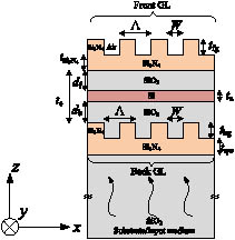
    Fig. 1. Sketch of the enhanced light-absorption structure that comprises a cavity-embedding Si layer, two GLs enclosing the cavity, and a substrate. The coordinate system is shown, where the grating periodicity and grooves/lines are along the x and y axes, respectively, and the layer stacking and light impinging directions are along the z axis.
    Sketchy flowchart of the optimization process. The GUI Module inputs the trial parameters, assessed as described in the text, fixed parameters, and constraints to the Optimization Module. There, the trial-and-error multi-start algorithm generates the next start points and inputs them into the Simulation Module, which feeds the algorithm back and loops until attaining an optimum.
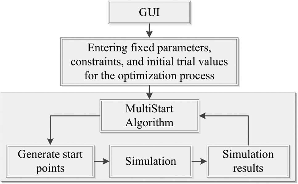
    Fig. 2. Sketchy flowchart of the optimization process. The GUI Module inputs the trial parameters, assessed as described in the text, fixed parameters, and constraints to the Optimization Module. There, the trial-and-error multi-start algorithm generates the next start points and inputs them into the Simulation Module, which feeds the algorithm back and loops until attaining an optimum.
    Efficiency spectra of the designed structures with a 0.15 μm thick Si layer. Broken lines: red, 2GL−TE1; green, 2GL−TM1; full blue line, 2DBR1. The structural parameters are found in Table 2.
    Fig. 3. Efficiency spectra of the designed structures with a 0.15 μm thick Si layer. Broken lines: red, 2GLTE1; green, 2GLTM1; full blue line, 2DBR1. The structural parameters are found in Table 2.
    Efficiency spectra of the designed structures with a 0.025 μm thick Si layer. Broken lines: red, 2GL−TE2; green, 2GL−TM2; full blue line, 2DBR2. The structural parameters are found in Table 2.
    Fig. 4. Efficiency spectra of the designed structures with a 0.025 μm thick Si layer. Broken lines: red, 2GLTE2; green, 2GLTM2; full blue line, 2DBR2. The structural parameters are found in Table 2.
    Electric and magnetic fields’ amplitudes squared (left ordinate) and Poynting vector modulus (right ordinate), normalized to the input |Sz|, across the cavity–absorber range of the dual-DBR structures: (a) 2DBR1; (b) 2DBR2. The intersections of the dashed lines with the abscissa mark the Si layer ends. Simulated at the CDW.
    Fig. 5. Electric and magnetic fields’ amplitudes squared (left ordinate) and Poynting vector modulus (right ordinate), normalized to the input |Sz|, across the cavity–absorber range of the dual-DBR structures: (a) 2DBR1; (b) 2DBR2. The intersections of the dashed lines with the abscissa mark the Si layer ends. Simulated at the CDW.
    Normalized to the input values, squared amplitudes of the EM fields versus 0≤x/Λ≤1 and z as defined in the text. (a), (c), (e) For 2GL−TE1: 0.22 μm≤z≤0.671 μm; x/Λ=0.426 is the internal grating lamella-groove interface derived line; (0,1)×(0.35 μm,0.5 μm) is the absorber cut within the microcavity. (b), (d), (f) For 2GL−TE2: 0.209 μm≤z≤0.679 μm; x/Λ=0.433 is the internal grating lamella-groove interface derived line; (0,1)×(0.412 μm,0.437 μm) is the absorber cut within the microcavity. Simulated at the CDW.
    Fig. 6. Normalized to the input values, squared amplitudes of the EM fields versus 0x/Λ1 and z as defined in the text. (a), (c), (e) For 2GLTE1: 0.22  μmz0.671  μm; x/Λ=0.426 is the internal grating lamella-groove interface derived line; (0,1)×(0.35  μm,0.5  μm) is the absorber cut within the microcavity. (b), (d), (f) For 2GLTE2: 0.209  μmz0.679  μm; x/Λ=0.433 is the internal grating lamella-groove interface derived line; (0,1)×(0.412  μm,0.437  μm) is the absorber cut within the microcavity. Simulated at the CDW.
    Normalized squared amplitudes of the (a), (b) electric and (c) magnetic fields’ components for the 2GL−TM1 structure shown versus 0≤x/Λ≤1 and 0.273 μm≤z≤0.631 μm as defined in the text. For a simulation convenience, the grating cell was inverted so that x/Λ=0.396 is now the grating lamella-groove interface derived line; (0,1)×(0.305 μm,0.455 μm) is the absorber cut within the microcavity. The normalization and simulation wavelengths are the same as in Fig. 6.
    Fig. 7. Normalized squared amplitudes of the (a), (b) electric and (c) magnetic fields’ components for the 2GLTM1 structure shown versus 0x/Λ1 and 0.273  μmz0.631  μm as defined in the text. For a simulation convenience, the grating cell was inverted so that x/Λ=0.396 is now the grating lamella-groove interface derived line; (0,1)×(0.305  μm,0.455  μm) is the absorber cut within the microcavity. The normalization and simulation wavelengths are the same as in Fig. 6.
    Maps of the EM power flow at the CDW in the structures (a) 2GL−TE1 and (b) 2GL−TE2 (Table 2). The quiver ranges are defined in Section 4, and the horizontal dashed lines show the material interfaces. The structure cut is shown in the inset to (a).
    Fig. 8. Maps of the EM power flow at the CDW in the structures (a) 2GLTE1 and (b) 2GLTE2 (Table 2). The quiver ranges are defined in Section 4, and the horizontal dashed lines show the material interfaces. The structure cut is shown in the inset to (a).
    Maps of the EM power flow at the CDW in the structures (a) 2GL−TM1 and (b) 2GL−TM2 (Table 2). The quiver ranges are defined in Section 4, and the horizontal dashed lines show the material interfaces.
    Fig. 9. Maps of the EM power flow at the CDW in the structures (a) 2GLTM1 and (b) 2GLTM2 (Table 2). The quiver ranges are defined in Section 4, and the horizontal dashed lines show the material interfaces.
    Possible placement of electrical contacts to the photoactive Si layer in the PD applications of the dual-GL structure, sketched in Fig. 1. The placement is appropriate for the BSI considered in this study as described in the text.
    Fig. 10. Possible placement of electrical contacts to the photoactive Si layer in the PD applications of the dual-GL structure, sketched in Fig. 1. The placement is appropriate for the BSI considered in this study as described in the text.
    Efficiency spectra θ dependence of the 2GL−TM2 structure. The structural parameters are found in Table 2.
    Fig. 11. Efficiency spectra θ dependence of the 2GLTM2 structure. The structural parameters are found in Table 2.
    Front standalone GL: (a) the original; (b) an effective-medium bilayer substitute.
    Fig. 12. Front standalone GL: (a) the original; (b) an effective-medium bilayer substitute.
    Back standalone GL: (a) the original; (b) an effective-medium bilayer substitute.
    Fig. 13. Back standalone GL: (a) the original; (b) an effective-medium bilayer substitute.
    λ0 [μm]Si3N4SiO2Si
    0.81.9962+i  01.4533+i  03.6925+i  0.0065
    Table 1. RIs at the CDW of the Materials that Are Set in the Text
    StructuretbgdbdftSi3N4tfgΛWηmaxQλRNt
    ta1=0.150
    2DBR10.0690.0300.808 (0.995)30333 (63)3.779 (7.346)
    2GLTE10.1200.1301.7100.7920.3050.4390.2520.999197.530.64273.307
    2GLTM10.1730.0321.7641.3800.2150.4680.1850.9991012.60.68473.814
    ta2=0.025
    2DBR20.0940.0530.353 (0.985)23029 (71)3.226 (8.220)
    2GLTE20.1090.2030.9680.2710.3220.4430.2510.999249.220.64471.998
    2GLTM20.5860.0031.2620.0470.4370.4790.1750.9955925.90.69672.460
    Table 2. Parameters of the Structures Designed Shown Below with Two Si Layer Thicknesses Outlined in the Texta
    Etching Errors2GLTE12GLTE2
    ΔWWΔtbgtbgΔtfgtfgΔλ0, nmΔηmax, %Δλ0, nmΔηmax, %
    +0.3+0.0+0.36+0.1
    ++0.3+0.0+0.26+0.1
    +−0.3−3.4−0.23−0.7
    ++−0.3−0.6−0.11−1.1
    ++0.4−0.3+0.32−0.6
    +++0.4−0.3+0.32+0.0
    ++−0.2−0.3−0.20−0.3
    +++−0.2−0.2−0.20−0.3
    Table 3. Performance Changes of the 2GL−TE Structures with Varying Grating Etch Parametersa
    Etching Errors2GLTM12GLTM2
    ΔWWΔtbgtbgΔtfgtfgΔλ0, nmΔηmax, %Δλ0, nmΔηmax, %
    +1.8−16.5−0.8−35.3
    ++1.8−8.3−0.7−53.3
    ++9.5−22.9+3.1−61.6
    +++9.5−18.9+3.6−7.5
    +−9.7−42.4−3.6−23.1
    ++−9.7−51.4−3.4−36.3
    ++−3.8−18.2+0.4−86.3
    +++−3.9−31.2+0.7−59.7
    Table 4. Performance Changes of the 2GL−TM Structures with the Varying Grating Etch Parametersa
    Roy Avrahamy, Moshe Zohar, Mark Auslender, Benny Milgrom, Shlomo Hava, Rafi Shikler. In-depth investigation and applications of novel silicon photonics microstructures supporting optical vorticity and waveguiding for ultra-narrowband near-infrared perfect absorption[J]. Photonics Research, 2020, 8(3): 381
    Download Citation