We propose a novel concept of designing silicon photonics metamaterials for perfect near-infrared light absorption. The study’s emphasis is an in-depth investigation of various physical mechanisms behind the ~ ultra-narrowband record peak absorptance of the designed structures, comprising an ultrathin silicon absorber. The electromagnetic power transport, described by the Poynting vector, is innovatively explored, which shows combined vortex and crossed-junction two-dimensional waveguide-like flows as outcomes of optical field singularities. These flows, though peculiar for each of the designed structures, turn out to be key factors of the perfect resonant optical absorption. The electromagnetic fields show tight two-dimensional confinement: a sharp vertical confinement of the resonant-cavity type combined with a lateral metasurface supported confinement. The silicon-absorbing layer and its oxide environment are confined between two subwavelength metasurfaces such that the entire design is well compatible with silicon-on-insulator microelectronics. The design concept and its outcomes meet the extensive challenges of ultrathin absorbers for minimum noise and an ultra-narrowband absorptance spectrum, while maintaining an overall very thin structure for planar integration. With these materials and such objectives, the proposed designs seem essential, as standard approaches fail, mainly due to a very low silicon absorption coefficient over the near-infrared range. Tolerance tests for fabrication errors show fair tolerability while maintaining a high absorptance peak, along with a controllable deviation off the central-design wavelength. Various applications are suggested and analyzed, which include but are not limited to: efficient photodetectors for focal plane array and on-chip integrated silicon photonics, high-precision spectroscopic chemical and angular-position sensing, and wavelength-division multiplexing.
1. INTRODUCTION
Enhancement of optical absorption is sorely sought in various light-management devices, such as solar photovoltaic and heat-storage cells and photodetectors (PDs), and it may also contribute to cutting-edge optical camouflage implementations. Silicon (Si) has such physical properties, including optical and electronic ones, that made it dominant in microelectronics and also a favorite for many photonic and optoelectronic applications, in particular those mentioned above. Broadly, Si photonics terms the field of prediction, design, fabrication, and implementation of photonic devices made of Si, its compounds with O and N, and with other IV-group elements. Often, this term is used in a narrower sense to refer to optical solutions to problems of connectivity and communication within a Si chip package by integrating Si-based optics and optoelectronics within the chip. Research on Si photonics began in the 1990s [1–5], proceeded through the 2000s [6–9], and has continued ever since [10–14]. On-chip optical interconnects require high-power lasers to convert the electrical data signals into light pulses, optical waveguides/fibers to propagate the light, and fast PDs to turn the optical signals back into electrical signals. Many breakthroughs have already been achieved [10–14] in the realm of diverse Si-based photonic and optoelectronic components.
From now on, the term PD is used for brevity to present any photo-absorbing device. Assume for simplicity that each photon absorbed by the photoactive layer of the PD generates an electron–hole pair. Then , where and are the quantum efficiency and optical absorptance, respectively, of the PD. In a monolithic PD, the detected light traverses the absorber once, so may be increased only by increasing its thickness , but the thicker the absorber, the stronger the thermal noise and the longer the transit time (in a diode PD). For some applications, e.g., PDs’ focal plane arrays (FPAs) [15], high and low noise are of paramount importance in order to show high responsivity while avoiding faulty high-density packaging. For others, e.g., the on-chip integrated Si-PDs (which should also be thin enough to be compatible with current planar-chip technology), the short transit time is also crucial.
A drastic decrease of to decrease the noise and transit time while maintaining high requires the confinement of incoming light around the absorber layer. An approach adopted to this end is based on the solid-state resonant Fabry–Perot cavity, in which this layer is sandwiched between two multilayered sections. In each of these, the distributed Bragg reflector (DBR) acts as a mirror and two layers adjacent to the absorber layer form an optical cavity. There, even very thin active layer may absorb most of the incident light power. Such a resonant-cavity enhanced PD (RCE-PD) [16] enables much more efficient (and faster, when relevant) detection, as well as operation at higher temperatures with a much thinner absorber than in its monolithic counterpart, although these benefits are traded off against a smaller spectral bandwidth.
Sign up for Photonics Research TOC. Get the latest issue of Photonics Research delivered right to you!Sign up now
The field of RCE-PDs has matured over the past decades regarding different spectral ranges, absorber materials, and physical devices; see, e.g., Refs. [3–6,17,18] for Si-PDs. However, the restriction on the DBRs’ reflectances [16] for attaining maximal peak may require deposition of too many layers, such that even with quite a thin absorber the entire device may prove too thick for on-chip integration. Such a high number of layers, as a rule, exceeds a technology-defined critical value, beyond which growth defects inevitably emerge and impair the device’s performance even with lossless DBRs; see, e.g., Ref. [19] for the ones. The reported on-chip Si-PDs, fabricated with thin but absorbing DBRs and rather large [3–6], showed very low NIR efficiency . Thus, reducing the Si RCE-PD thickness below some threshold clearly conflicts with the perfect- objective.
Due to the reasons outlined above, to concurrently meet the challenges of a high , thin Si layer, and small overall thickness of a NIR Si-PD, a new design solution, quite different from the RCE approach, is needed. We suggest using metasurfaces [20], which enable us to redesign the known photonic devices to make them thinner and planar while concurrently being of a highly reduced complexity and a high performance. For our purposes, we use the simplest kind of metasurface, a subwavelength (SW) grating-on-layer (GL) metasurface. So far, an upgrade of the RCE-PD with the replacement of the front DBR by a one-dimensional (1D) GL (not necessarily an SW one) was proposed, and proof-of-concept examples of the thus modified HgCdTe-PDs were reported [21,22]. The round-trip phase control [16] extended to account for the presence of the grating and an optimization allowed for [21,22] fabrication-tolerant designs with peak and a back DBR twice as thin as that of the best performing RCE-PD composed of the same materials. However, due to the remaining DBR, such a design solution proves yet insufficient for downscaling the Si-PD at goal.
In Si photonics, a diffraction order grating was theorized [1] to bend normally incident light into the depletion region of the on-chip Si-PD. Another efficient light coupling into a CMOS-compatible Si-PD was demonstrated; see, e.g., Ref. [7], with a Si–air grating under oblique incidence, at which only one nonspecular diffraction order is supported. A similar strategy is followed [13,14,23] in contemporary Si photonics. In several important applications, the high-refractive-index (RI) contrast SW-GL, despite its structural simplicity, may function like a much more complex metasurface [20]. Due to this fact, such SW-GL nowadays attracts much interest [24] as a new platform for integrated optoelectronics, in particular, Si photonics [13,14].
In this study, novel ultrathin Si-photonics structures are proposed and designed to show strikingly efficient light absorption within a narrow portion of the NIR range, around the center-design wavelength (CDW) μ. In theoretical studies [1], this wavelength was allocated as one from operation bandwidths of on-chip NIR Si photodiode PDs [3–5,7,9], implying that a short-haul light guiding with Si [10–13] is still feasible at . Remarkably, these structures exhibit strong vortex and waveguide flows of the internal electromagnetic (EM) power as outcomes of the EM fields’ singularities [25].
The rest of the paper is organized into six sections. Section 2 states the problem, outlines the suggested structures, and discusses their modeling. In Section 3, an optimization-based design procedure is described, and the considered structural parameters and computed absorptance spectra are presented. In Section 4, the simulations of the EM-fields-related physical quantities at the CDW are reported, and their results are discussed. Section 5 reports the designs’ tolerance testing results. Section 6 considers possible applications of the designed structures, and Section 7 concludes the study.
2. STATEMENT OF PROBLEM, PROPOSED ENHANCED ABSORPTION STRUCTURES, AND PRINCIPLES OF MODELING
In the quest to thin the Si-photonics structure as much as possible, it will perfectly absorb light at the designated NIR CDW while surpassing the bounds on the mirrors’ and cavity’s thicknesses noted in the introduction. We redesign the RCE structure by replacing both DBR mirrors by 1D GL with the same grating period . Since and are well technologically compatible with each other and Si for composing the DBR and the cavity [19], respectively, we employ these materials in the redesign, while benefiting from the previous design technique [21,22] to attain nearly perfect peak absorptance.
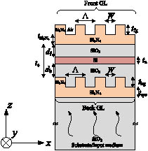
Figure 1 shows a schematic of the dual-GL structures under study. There, the cavity and substrate material is , and the front air– with the back GL encloses the cavity. As shown in Fig. 1, we consider the through-substrate backside illumination (BSI) at normal incidence. Benefiting from the absence of the backside electrical contacts, BSI has the essential advantage of reducing the PD pixel size without decreasing the amount of input light power [26], which is desirable for on-chip applications.
Figure 1.Sketch of the enhanced light-absorption structure that comprises a cavity-embedding Si layer, two GLs enclosing the cavity, and a substrate. The coordinate system is shown, where the grating periodicity and grooves/lines are along the and axes, respectively, and the layer stacking and light impinging directions are along the axis.
In this paper, we adopt the modeling, which simplifies the design to one in which only the optics need to be considered. Herewith, rather than being restricted to a specific PD technology, we analyze the structures optically, characterizing the constitutive layers by complex RIs , where are the real RIs and are the extinction coefficients. This modeling still has widespread use for initial designs of the electronic PDs [16,18,21,22,26,27]. In such cases, optical modeling can be complemented and refined by an electron-device simulation [18,28,29]; however, it is not expected to disprove the optical modeling outcomes. The and spectra for the involved materials are found in Refs. [30–32]; their values at the CDW are given in Table 1.
λ0 [μm]
Si3N4
SiO2
Si
0.8
1.9962+i0
1.4533+i0
3.6925+i0.0065
Table 1. RIs at the CDW of the Materials that Are Set in the Text
Here, the design emphasis is put on obtaining the maximal CDW efficiency , while maintaining constant per design, and keeping the back-GL cladding’s thickness (similarly to the DBR layers’ thicknesses) fixed at the quarter-wave value . Such dimensions as and the groove width (constrained for simplicity to be the same for both GLs), etch depths and , as well as the thicknesses of the front-grating cladding and front and back cavities, and , respectively, are the design variables. We observe the SW regime, limiting ab initio the operation wavelengths from below by the Rayleigh wavelength , which suppresses the non-specular orders of the grating diffraction into the cavity and so prevents losses due to light escaping from the structure’s sides. Note that this is not compulsory since the non-specular orders can be suppressed with extra constraints; see, e.g., Refs. [21,33].
3. DESIGN PROCEDURE, OPTIMAL STRUCTURES, AND THEIR EFFICIENCY SPECTRA
We perform the computer-aided designs with an in-house software run in MATLAB environment. The software consists of two modules: “Simulation,” which contains the codes of an in-house recast rigorous coupled-wave analysis (RCWA) for simulations of the structures merging smooth and grating-patterned layers as described in detail elsewhere (see Ref. [21] and references therein); and “Optimization,” which calls a multi-start optimization algorithm from MATLAB Optimization Toolbox [34–36] and a graphical user interface (GUI), which forces the modules to interact and thus drives the simulations and designs as shown in Fig. 2.
Figure 2.Sketchy flowchart of the optimization process. The GUI Module inputs the trial parameters, assessed as described in the text, fixed parameters, and constraints to the Optimization Module. There, the trial-and-error multi-start algorithm generates the next start points and inputs them into the Simulation Module, which feeds the algorithm back and loops until attaining an optimum.
In order that the optimization would not be blind, we are guided by an approach to obtaining initial (start, trial) design parameters that, in modern terms, are geometric-phase control [20]. Homogenizing the gratings as described in Appendix A, we first design the front and back GLs to be standalone and to be highly and lowly reflective (subsections A and B), respectively, at a normal CDW incidence from a semi-infinite . In this way, we assess trial values , , , , for the GLs’ parameters shown in Fig. 1. With these, our RCWA code returns the GLs’ reflection-amplitudes’ phases and , the sum of which gives a rough idea on the geometric phase of an unloaded dual-GL cavity. leads us to estimate for such cavity’s thickness with the round-trip phase condition ; see, e.g., Refs. [16,27]. Though the Si layer is not involved in the start design, the cavity in the final design does adopt it (see Section 2), so given a , we hold the bound by tuning . Finally, the front and back cavity thicknesses, but not (see Fig. 1), are optimized with initial values , , chosen compatible with the relation , where we take for simplicity. The start equality proves a posteriori far from the relation between and for the optimized dual-GL structures but much closer to that for the optimized dual-DBR structures.
Due to the very small extinction of Si in the operation range [see in Table 1], it might be expected that the Si layer would not be too thin; see, e.g., Refs. [3–5]. In fact, due to Ref. [27], we figured out two initial values of for optimizing the dual-DBR structure μ and μ. To ultimately maximize , these values were finally refined by the optimization process to μ and μ. These were used among the fixed input parameters in optimizing the dual-GL structures (see Fig. 2) to attain . The results of the computer-aided optimal design, with two Si layer thicknesses indicated above are shown in Table 2; the spectra are shown in Figs. 3 and 4.
Structure
tbg
db
df
tSi3N4
tfg
Λ
W
ηmax
Q
λR
N
t
ta1=0.150
2DBR1
—
0.069
0.030
—
—
—
—
0.808 (0.995)
303
—
33 (63)
3.779 (7.346)
2GL−TE1
0.120
0.130
1.710
0.792
0.305
0.439
0.252
0.999
197.53
0.642
7
3.307
2GL−TM1
0.173
0.032
1.764
1.380
0.215
0.468
0.185
0.999
1012.6
0.684
7
3.814
ta2=0.025
2DBR2
—
0.094
0.053
—
—
—
—
0.353 (0.985)
230
—
29 (71)
3.226 (8.220)
2GL−TE2
0.109
0.203
0.968
0.271
0.322
0.443
0.251
0.999
249.22
0.644
7
1.998
2GL−TM2
0.586
0.003
1.262
0.047
0.437
0.479
0.175
0.995
5925.9
0.696
7
2.460
Table 2. Parameters of the Structures Designed Shown Below with Two Si Layer Thicknesses Outlined in the Texta
Figure 3.Efficiency spectra of the designed structures with a 0.15 μm thick Si layer. Broken lines: red, ; green, ; full blue line, . The structural parameters are found in Table 2.
Figure 4.Efficiency spectra of the designed structures with a 0.025 μm thick Si layer. Broken lines: red, ; green, ; full blue line, . The structural parameters are found in Table 2.
While the planar-interface layers are insensitive to the polarization of normally incident light [37], the 1D gratings (see Appendix A) are strongly sensitive to it. Hence, given a , the design yields at least two different dual-GL structures, i.e., those for the TE- or TM-polarized irradiation, when the incident electric or magnetic field is overall along the grating grooves, respectively. To have an idea up to what extent they improve the efficiency over the RCE structure, we optimized the latter with the DBRs at both sides, using the same technique, while keeping its overall thickness comparable with those of the dual-GL structures. Releasing this constraint, the optimal dual RCE structures reach CDW absorptance at the cost of a huge number of layers (parenthesized in Table 2), which makes them technologically unfeasible. Further, we refer to the thus optimized structures as 2GL−TE, 2GL−TM, 2DBR, and .
Table 2 and Figs. 3 and 4 show that the thinner the absorber, the higher the relative gain in of the designed dual-GL structures compared to and . It can be inferred from Figs. 3 and 4 that, as regards the full width at half-maximum (FWHM) , the spectra of the 2GL−TE and 2GL−TM are the widest and narrowest, respectively, whereas for the RCE structure, is in between them, with the same absorber thickness . It seems that the spectra of the optimized dual-GL structures get sharper and narrower as decreases; the extremely small spectrum of the in Fig. 4 is notable. Due to the definition of the damped-resonator quality () factor , the factors for the designed structures are easily assessed from the data of Figs. 3 and 4. The estimated values are displayed in Table 2 and prove rather high, especially for the TM structures. Note that on-chip Si RCE-PDs were fabricated [5,6] with that are quite larger than those of the ; see Table 2. An RCE-PD with the front and back DBRs [5] showed at , and for one with only back DBR [6] it was at 0.86 μm, which is notably smaller than the of ; see Table 2.
4. ELECTROMAGNETIC FIELDS AND POWER FLOW
It is worth noting that all the studied structures, laterally unlimited (actually, huge times wide) and several times thick, are three-dimensional (3D) structures. In this regard, our simulations are 3D, though they are simplified by the independence of the EM fields on for the dual-GL structures (as with, e.g., all RCWA-based simulations), or on , for the dual-DBR ones, which does not imply any two-dimensional (2D) or 1D spatial confinement. The light confinement in the cavity–absorber region, mentioned in the introduction for the RCE structures, and that for the dual-GL ones—both discussed and quantified in this section—is entirely related to the EM fields.
In the RCE structures, the EM confinement is built up due to the optical resonance in a cavity enclosed by plane-parallel mirrors [16,27] and so are 1D in essence. Since the dual-GL structures under study are assemblies of identical vertical () top-to-substrate microscale cuts of width from the structure shown in Fig. 1, another physics, which is an EM field resonant recirculation in micro/nanoscale areas or volumes on the sub-wavelength scales [38], might be more suitable for them. We view the above cut as a “microcavity”; the quotes indicate that it has no real vertical boundaries. Inside the microcavity, the lamella-groove boundary line marks an actual materials interface in the grating regions; continued outside them is a dummy, reminiscent of the above real boundary. The nano/microcavity reasoning has been adopted previously for a simpler grating-based optical resonator [39] and 2D photonic crystal slabs [40]. While the physics in the RCE devices, behind the EM confinement, is well understood, e.g., Refs. [16,27], its current understanding for the micro/nanocavity devices is much less mature and is more particular per structure. In these cases, visualizing the electric () and magnetic () fields and Poynting vector (), computed at the CDW, may shed light on the near-field EM recirculation and thus portray the confinement and power flow ad hoc. Doing that for the dual-DBR structures aims primarily at confirming the adopted vision [16,27]. For any layer, a rigorous relation between and states that is the difference between surface-averaged normal components of (power fluxes) at the layer’s exit and entry.
For the , in which the only nonzero components , , and depend only on , we plotted , , and versus in Fig. 5. As is seen, while is slightly sub-linear in one half and super-linear in the other half of the absorber of , it is visibly linear throughout the absorber of . Overall, , which is due to high RI contrast between and Si; see Table 1. In the absorber layers, the maxima of and minima of , and vice versa, are complementary.
Figure 5.Electric and magnetic fields’ amplitudes squared (left ordinate) and Poynting vector modulus (right ordinate), normalized to the input , across the cavity–absorber range of the dual-DBR structures: (a) ; (b) . The intersections of the dashed lines with the abscissa mark the Si layer ends. Simulated at the CDW.
In the dual-GL TE or TM structures, or , respectively, and . Hence, we plotted the surface graphs of the appropriate squared modules of these fields’ components versus in Figs. 6 and 7. These show the continuity of [Figs. 6(c), 6(d), 6(e), 6(f), 7(c)], [Figs. 6(a) and 6(b)], and [Fig. 7(a)], and the discontinuity of [Fig. 7(b)] when crossing the cavity–absorber interfaces, which is in fair agreement with the EM boundary conditions. Also, the quiver maps of are plotted in Figs. 8 and 9. Due to the a priori periodicity of , , and , restricting the to within any segment of length , not necessarily , is sufficient to pick out the microcavity. For reasons of scale and convenience, is also restricted to a lateral slice of the microcavity. Due to a perfect-mirror action of the front GL, the EM fields strongly decay there, and hence it is overall excluded from the scope. In Figs. 6 and 7, the range covers such parts of the absorber–cavity region, in which the front cavities are top cut to 10% and 25% of their thickness for and , respectively. In Figs. 8 and 9(a), the range is extended to also include the back GL. The range in Fig. 9(b) includes a part of the absorber–cavity region, where the front cavity is top cut to retain 5% of its thickness and top 5% of the back grating range.
Figure 6.Normalized to the input values, squared amplitudes of the EM fields versus and as defined in the text. (a), (c), (e) For : μμ; is the internal grating lamella-groove interface derived line; μμ is the absorber cut within the microcavity. (b), (d), (f) For : μμ; is the internal grating lamella-groove interface derived line; μμ is the absorber cut within the microcavity. Simulated at the CDW.
Figure 7.Normalized squared amplitudes of the (a), (b) electric and (c) magnetic fields’ components for the structure shown versus and μμ as defined in the text. For a simulation convenience, the grating cell was inverted so that is now the grating lamella-groove interface derived line; μμ is the absorber cut within the microcavity. The normalization and simulation wavelengths are the same as in Fig. 6.
Figure 8.Maps of the EM power flow at the CDW in the structures (a) and (b) (Table 2). The quiver ranges are defined in Section 4, and the horizontal dashed lines show the material interfaces. The structure cut is shown in the inset to (a).
Figure 9.Maps of the EM power flow at the CDW in the structures (a) and (b) (Table 2). The quiver ranges are defined in Section 4, and the horizontal dashed lines show the material interfaces.
It appears that, when simulating , , and for the microcavity frame , the , surfaces and flow maps prove asymmetric as regards their boundaries-adjoined critical features (see further in the present section). An analysis shows that the symmetry is restored while preserving the graphs’ topology, with applying a rigid lateral shift of the microcavity frame by the distance ; note that for symmetric grating structures with . Table 2 affords the following values of : (), () and 0.06891 (), 0.06769 (), so the shift is to the right for , and the shift is to the left for . Thereby, the EM fields and Poynting vector were recomputed for the shifted frame, and Figs. 6–9 show the resulting , surface graphs and quivers. In all the following figures and discussions, still denotes the lateral coordinate, and bare values of the microcavity lateral boundaries, i.e., 0, , are assigned to the respective shifted boundaries.
A. Dual Grating-On-Layer TE Structures
1. Electric and Magnetic Field Amplitudes
For and , the plots of , , and shown in Figs. 6(a), 6(c), 6(e), and Figs. 6(b), 6(d), 6(f), respectively, display highly peaked surfaces. It is found that the minimum -direction distance between each two peaks is 0.5, in units of , as may be expected from the periodicity. The bell-shaped and surfaces are strictly confined inside the microcavity. They have four and two peaks located at the cavity–absorber interface lines and inside the absorber, respectively, for , and vice versa for the .
As seen in Figs. 6(e) and 6(f), the surfaces show three pairs of peaks for and three peaks for , respectively. One of the peaks (pairwise or singular) is internal, whereas the two others adjoin the vertical boundaries of the microcavity. The surface(s) adjoined to one boundary is (are), as expected, strictly symmetric to the one(s) adjoined to the other boundary, attaining there their maximums. In , the peaks of and lie on the cavity–absorber interface lines [see Figs. 6(a) and 6(e)]. The peaks of lie on the midline of the absorber (μ); see Fig. 6(c). In , the situation is just the opposite; here the absorber is much thinner than in the , so that in order to provide resonant absorptance, tends to be as large as possible, which pushes out of the absorber. The maximums of , at the vertical microcavity boundaries, over the corresponding ranges in Fig. 6, are about 1.24, 1.29 and 1.58, 1.50 for and , respectively. In , has the absolute maxima at the crossing points of two vertical midlines between the lamella-groove interface-derived line and microcavity boundaries with the horizontal absorber–cavity interface lines, while has the absolute maxima at the crossing points of the same vertical lines with the absorber’s midline. In , the maxima points of these functions are swapped.
In view of the location and sharpness of the and peaks, the tight vertical-by-lateral 2D EM fields’ confinement occurs in each microcavity of both structures. Moreover, because the above boundary values of , , relative to their global maximums, are about , for , and , for , the microcavities in both structures come close to electric and lateral-magnetic isolation. In Figs. 6(e) and 6(f), we observe that the internally peaked surface’s parts are confined similarly to the and surfaces. Because of the boundary-peaked parts of the surface, penetrates from a given microcavity to any one adjacent to it, so there is no vertical magnetic isolation of the microcavities.
2. The EM Power Flow
In Figs. 8(a) and 8(b), we visualize the EM power flow in and , respectively, using the quiver plots of . The figures display the Poynting vector distributions of those structures, demonstrating vortex-like flows. Both flows consist of two vortices, a central one with counterclockwise circulation and the other, which is split into two symmetric parts adjacent to the microcavity boundaries with clockwise circulation, so that the total circulation appears to be zero. The distance between the vorticity centers is , as expected from the periodicity of . When moving along the axis through the microcavity, consistently switches its sign at the vertical lines of and . The continuity of dictates that these lines are also the lines of the minima. The inner vortices’ centers lie on the midline of the microcavity , and the boundary-adjoined vortices are centered at the vertical boundaries of the microcavity. For both structures, the vortices are strictly confined between the lateral boundaries of the chosen microcavity slices. Contrary to the inner vortices, the boundary-adjoined ones are unconfined laterally and percolate continuously from the given microcavity to the neighboring ones.
Both vortices in [Fig. 8(a)] consist of two linked sub-vortices sustaining the above noted respective circulations, which correlates clearly with the pairwise peaks of in Fig. 6(a) and of in Fig. 6(e). Figuratively speaking, the vortices start the circulation at the back cavity–absorber interface, stretch vertically to the absorber layer, and make the counter-circulation turn at the absorber–front cavity interface. Between the vortices and apart from their vicinity, the EM power flow inside the absorber layer is dominantly vertical. It crosses the absorber back and forth as a result of the reflection from the GLs. The combination of the vertical flow alongside the lateral one at the vortices’ closure seems to be the key mechanism of the peak absorptance of this structure. Four additional singularities appear at the back grating region, two of which are vortices, and the other two at and are seemingly flow junctions. The left junction seams to channel a lateral power that flows into it from opposite directions (left and right) to a vertical one that flows away from it, also in opposite directions (up and down), whereas the right junction does exactly the opposite.
The vortices in [Fig. 8(b)] do not cluster into sub-vortices, and the flow they carry circulates entirely inside the back cavity. Between the vortices and apart from their close vicinity, the flow is dominantly vertical and is pumped into and out from the absorber layer via the vertical junctions, the midlines of which are again and , respectively. Such an EM power transfer produces lateral waveguide-like right and left flows inside the absorber layer slice within the microcavity. As seen in Fig. 8(b), the right flow occurs between the junctions’ entrances and is restricted within the microcavity, whereas the left flow is piecewise inside and and is responsible for the EM power transfer between the periodically arranged microcavities. This lateral back and forth flow is the main absorption enhancement mechanism for . The reason why the lateral flow occurs in the absorber layer of this structure and does not in that of is the very small thickness of the former layer, 6 times smaller than that in ; it appears that with such a thin Si layer, a planar trilayer will guide only a single light mode. Although the light-absorption enhancement mechanism in the structure differs notably from that in the previously discussed one, it also provides peak absorptance. Note that the flow at the back grating region is very similar to that of , which seems to be due to the closeness of their dimensions. Originating at the back grating, this mixed lateral-vertical flow supports the EM energy confinement and channels the EM power in the microcavity of both TE structures.
A spectral deviation from the optimal CDW or an alternation of the structure’s optimal dimensions, such as the grating parameters and the absorber thickness, which result in a change of the optical properties, affects the overall and absorber flows (direction and/or magnitude) and the singular points (location and/or existence). In the structure, for example, the decrease in absorptance due to these variations is noted as breaking the absorber’s balanced lateral optimal flow and the vortices’ existence and location. Note that the vortices do not appear only in the optimized structures and not discretely at the CDW. Still, moving further away from peak resonances and confinement wavelengths, by changing the incident wavelength or optimal dimensions, conventional flows of no vorticity are likely to be observed.
B. Dual Grating-On-Layer TM Structures
1. Electric and Magnetic Field Amplitudes
The plots of , , and for shown in Figs. 7(a)–7(c), respectively, also display the surfaces that are highly peaked but topologically very different from those for the dual-GL TE structures considered above. It is seen that the surface (disregarding the back cavity layer), similarly to the one in Fig. 6(a), consists of four highly peaked regions. However, here two of the surface peaks are relatively weak and sharp, with maximums located at the absorber–front cavity interface, and two others are strong and less sharply peaked inside the absorber layer. In contrast with the plot, the peaks of the plot in Fig. 7(c) are asymmetric relative to the absorber layer. Nevertheless, with an appropriate interchange , several properties of the present plots in Fig. 7 seem to comply with those in Figs. 6(a),6(c), and 6(e). Namely, the shortest -direction distance between each two maximum pairs of both and , and minima of , is . Also, a strong resemblance between the and plots can be seen when comparing Fig. 6(c) to Fig. 7(a). Similarly to the 2GL−TE cases, the two , maximums lines are at and , and the same holds for the minima lines.
The above asymmetry along the axis may be attributed to the very small thickness (32 nm) of the back cavity layer (see Table 2), in which the following dissimilarity between the TE and TM structures is observed. While all the above discussed EM field amplitudes in the dual-GL cavity TE structures (Fig. 6) increase when progressing up along the axis, i.e., moving right to left in the figure inside the back cavity layer towards the absorber interface, the EM fields for decrease along the similar path. An additional dissimilarity is found in the above-noted discontinuity of as seen in Fig. 7(b). Inside the absorber drops times at most, but it still peaks there up to relative units, which concurrently with high provides peak absorptance. Due to a close similarity to the fields and to avoid repetitions, the fields are not shown. However, the EM power flows and the absorption mechanisms of both structures, which appear to be quite different, are discussed in the next subsection.
2. The EM Power Flow
The EM power flow quiver of the is shown in Fig. 9(a); for convenience, the flow in the absorber and front cavity regions is scaled and displayed in the inset. This time the dominant vortices are vertically centered at the back GL region, one at the -axis center and the other split between the boundaries, similar to the cavity–absorber region vortices in the TE case (Fig. 8). Inside the chosen microcavity, no strictly confined vortices are observed. In the present structure, the back cavity layer is the thinnest one, and it is not surprising that, similar to the case of the absorber layer in , a mostly lateral flow occurs within it. A similar flow proceeds at the lower [upper in Fig. 9(a)] part of the absorber layer, though it is about 6 times less intense due to the discontinuity of in , while crossing the back cavity–absorber interface μ, quantitatively resulting from the discontinuity ; see Fig. 7(b). For the same reason, a similar “jump” of occurs when crossing the absorber–front cavity interface μ, which is seen in Fig. 9(a). This behavior contrasts with the overall continuity of in and .
In this case, the strong lateral flow in the back cavity layer originates from the EM power pumping out and into the vortices that persist in the back GL region (not shown here). As seen in Fig. 9(a), the inter-layer transfer of the EM power goes down and up via the above junctions along the and midlines, respectively. Although the flow over the upper [lower in Fig. 9(a)] part of the absorber is negligibly small as compared to that in the rest, the predominantly lateral flow over the latter proves sufficiently strong to provide the perfect optical absorption.
Focusing mainly at the absorber and its closer regions, the EM power flow of the structure is shown in Fig. 9(b). As for the previous structures, a laterally centered and a boundary split vortices are displayed, only this time they are both vertically centered inside the absorber layer. Both vortices are stretched vertically throughout the entire absorber layer and close at the cavity layers. The vortices’ closure echoes vertically deep and laterally wide into the back GL and front cavity regions; actually, it appears that the stretched singularity inside the absorber is replaced by a wide lateral flow outside the absorber layer. Between the vortices and apart from their closest vicinity, the EM power flows almost completely vertically up and down inside the absorber. So although it is ultrathin, the high electrical fields and the back and forth flow inside the absorber layer fuel the peak absorptance.
To conclude the section, maximizing the absorptance peak at the CDW dictates the vortices centers’ locations and the waveguide-like flows within the structures in general, and inside the active layer in particular, which allows attaining the . Let us stress a generic difference between the EM confinement and power flow in the dual-DBR (RCE) and dual-GL structures. Namely, in the former, due to the lateral interfaces, light paths are 1D vertical round-trips along the axis; see Fig. 4. The lateral and vertical interfaces in the latter concurrently force light to flow along complex 2D paths in the plane; see Figs. 8 and 9. For the dual-DBR structures, the zero EM field singularities have little effect on , which is a rather plain function of , as seen in Fig. 5. However, the EM field zeros in the dual-GL structures, seen in Figs. 6 and 7, do complicate the flow, which manifests itself in diverse topological structures, e.g. vortices, shown in Figs. 6 and 7.
5. DESIGN TOLERANCES
The issue of fabrication tolerances is of primary practical importance in the design of the proposed structures. Since in the manufacturing of these devices only few-layer deposition steps are required, the grating fabrication accuracy is critical. For the dual-GL cavity-enhanced photo-absorbers under study, we carried out the performance tolerability tests, varying , , and around their optimal values in Table 2. We adopted relative error in all the etch parameters for the and structures. However, with these, and even twice as small etching errors, the structure looses its absorptive performance. Due to that, we inquired about the performance of this structure against relative etching error.
Tables 3 and 4 display the test results for the designed TE- and TM-polarization targeted structures, respectively. Table 3 shows that the structures sustain high performance, i.e., exhibit a small peak-efficiency deterioration concurrently with a tiny peak-wavelength shift on a sub-nanometer scale. Particularly, apart from one exceptional case for each structure, such as with and for and , respectively, all other combinations of the errors result in a less than 1% deterioration.
Etching Errors
2GL−TE1
2GL−TE2
ΔWW
Δtbgtbg
Δtfgtfg
Δλ0, nm
Δηmax, %
Δλ0, nm
Δηmax, %
−
−
−
+0.3
+0.0
+0.36
+0.1
−
−
+
+0.3
+0.0
+0.26
+0.1
−
+
−
−0.3
−3.4
−0.23
−0.7
−
+
+
−0.3
−0.6
−0.11
−1.1
+
−
−
+0.4
−0.3
+0.32
−0.6
+
−
+
+0.4
−0.3
+0.32
+0.0
+
+
−
−0.2
−0.3
−0.20
−0.3
+
+
+
−0.2
−0.2
−0.20
−0.3
Table 3. Performance Changes of the 2GL−TE Structures with Varying Grating Etch Parametersa
Similar testing of the structures shows that they still support resonant absorption all over the tests, though with essentially larger , as seen in Table 4. It is also seen that with the same relative errors, deteriorates in the performance one and a half orders of magnitude stronger than . For , except for two severe deterioration cases with and (at both ), at the other errors’ combinations, , which means a still reasonable tolerance. The high performance sensitivity of the 2GL−TM structures, sharper for the , also correlates well with their superior factors (see Table 2) and may be attributed to an alternating charging of the line-groove interfaces by the light electric field component that emerges only in the TM polarization. To shed more light on the above noted deterioration cases for , we inquired how a error in only, with the other dimensions kept at their optimal values, affects the peak absorptance and flow. We found that , so just such an error holds a dominant contribution to those cases, while the errors in when switched on concurrently can either enhance or reduce the deterioration as seen in Table 4. Also, at only , two vortices, managing the EM power flow back to the absorber at the optimal dimensions, disappear (not shown). Instead, the power continues to flow up, and the optimal confinement is disturbed to a large extent. Table 4 shows that for the performance tolerance issue is problematic; in a half of the etch errors’ combinations it exceeds 50%, rising up to in the worst case. This is not surprising due to its highest factor and very specific EM confinement mechanism, which are extra sensitive to the structural dimensions.
6. APPLICATIONS
Due to Table 2, the designed Si-photonics structures appear to be loaded in high--factor and -peak-absorptance resonators for the chosen , and quite similar design can be carried out for any higher NIR wavelength below 1 μm. Hence, due to their high efficiency and ultra-small thickness, these proposed structures can be used as efficient and thin PDs in FPAs, on-chip integrated Si photonics, and precise spectroscopic chemical sensing. When unloaded, the designed double-GL cavities exhibit a narrowband transmission notch at , so they may be used as ultra-narrowband optical filters for a wide range of applications.
For the PD applications, electrical contacts need to be connected to the Si layer. Close methods to this end were developed for RCE-PDs, both photodiode and photoconductor ones, e.g., Refs. [3] and [28,41], respectively, and waveguide-coupled PDs, e.g., Refs. [7,23]. Briefly, the technique amounts to ad hoc making the part below the front cavity wider than that above the Si layer, on both sides in the direction, and then depositing the poly-Si/metal contacts atop the protruding Si strips as shown in Fig. 10. Since the structures are a huge times (in our case, also ) wide, the results obtained without the width offset prove valid with it as experimentally verified [26,28,41].
Figure 10.Possible placement of electrical contacts to the photoactive Si layer in the PD applications of the dual-GL structure, sketched in Fig. 1. The placement is appropriate for the BSI considered in this study as described in the text.
Upon an offset of the light incidence from the normal to an oblique small angle , the absorption peaks split into two peaks at some and for the TE structures and shift to positions at some for the TM structures; see the example in Fig. 11 for . The splitting and shift fit accurately with linear and quadratic regressions, respectively, viz. and . Here and , each with less than 2% maximum standard relative error, equal 9.818 nm/deg for , 16.19 nm/deg for , for , and for . Both and performances can be easily calibrated, provided that the quantities are measurable. Thus, the considered dual-GL cavity structures may be used for high-precision angular-position sensing.
Figure 11.Efficiency spectra dependence of the structure. The structural parameters are found in Table 2.
The above noted sensitivity to a varying incidence angle may also be beneficial for the WDM, highly important in contemporary optical communication. The exponential growth in the need for ultra-fast and ultra-wideband communication stimulated the development of the WDM. It provides an increase of the capacity by multiplexing a number of optical carriers using multiple wavelengths onto a single optical guide. With the existing electrical and optical infrastructure for long-haul communication, the WDM approach has proven to be highly cost effective and to benefit, for an efficient operation, from such optical components as ultra-narrowband transmitters, receivers, and filters.
The evolving DWDM requires channel separation that can reach higher than 50 GHz in frequency or lower than 0.8 nm in wavelength. This demands ultra-narrow and stable components acting as demultiplexers to separate each wavelength with minimum crosstalk. Structures such as those proposed and designed in this work can help address this challenge due to their high , , and sensitivity. A possible approach for separating the wavelength channels is directly by the dependence of the absorptance spectra on . For example, as can be inferred from Fig. 11, provides separation around 0.8 μm. Though our structures can function as DWDM devices only for integrated-circuit short- to medium-haul communication in the range μμ, principles quite similar to those developed in this work can be applied for a higher efficiency redesign of the detectors currently in use for the conventional communication band’s DWDM, such as the monolithic InGaAs.
The emerging field of optical camouflage would also benefit from designs inspired by light-absorbing structures such as those considered in this study, which are ultrathin, subwavelength, and perfectly absorptive. For this purpose, managing the light power to flow laterally in a thin buried absorbing channel, as Figs. 8(b) and 9(a) demonstrate, seems indispensable.
7. CONCLUSIONS
We proposed and theoretically investigated a new type of enhanced light-absorption structures for NIR Si-photonics (see Table 2), comprising only Si-microelectronics-compatible materials ( and ) and Si (see Table 1) as the NIR light absorber, in contrast with, e.g., Refs. [5,6]. Inspired by the RCE-PD, this structure contains the cavity–absorber (Si) wrap enclosed with the subwavelength GLs. We argued that the assembly of the RCE-PD with the same materials and topmost absorptance is beyond the scope of feasibility. On the contrary, the subwavelength dual-GL cavity enhanced ultrathin structures, attaining ultra-narrowband peak at the near IR, were shown to be feasible with the in-house software design.
We extensively shed light on the multiple physical mechanisms behind the record of the designed structures, visualizing the resonant EM field amplitudes and power flow over the important space regions inside the structures. We concluded that the EM fields in the cavity–absorber region are tightly 2D confined, which combines the sharpened vertical confinement of the resonant-cavity type with lateral confinement set by the GLs’ derived microcavity. Also, we gave novel comprehensive and structure-peculiar insights into the EM power transfer, which combines vortex and junction crossed waveguide-like flows. The flows point at optical singularities, at which , such as the vorticity centers and junctions, which connects this study to singular optics [25]. These combined singular optical phenomena proved to be the keys to the perfect optical absorption of each of the designed and simulated structures. Furthermore, we tested the structures’ performance tolerances to the grating fabrication errors, and found them to be superlative for ; see Table 3. Among the TM-polarization targeted dual-GL enhanced structures, tolerates most of the errors an order of magnitude weaker than its TE-polarization counterpart, still exhibiting a practical performance.
Finally, in Section 6, we discussed at length possible applications of the proposed structures. To our knowledge, using the metasurfaces proposed and scrupulously theoretically investigated in this study conceptually advances design of topmost optical-absorption structures. Last but not least, this study brings a new focus on striking features of the EM field distribution and Poynting vector flow over the metasurfaces-confined micro-structures. The design principles and subsequent analyses developed in this study may be implemented in other fields of the micro- and nano-optics research and applications.
APPENDIX A: GRATING-ON-LAYER DESIGN
Starting values of the GLs’ parameters, needed in the computer-aided design input as shown in Fig. 2, are obtained using a trial semianalytical design on the basis of effective-medium and grating-waveguide resonance theories. In these designs, we approximate the true standalone GLs shown in Figs. 12(a) and 13(a) by effective bilayers as shown in Figs. 12(b) and 13(b), respectively, in which the binary-grating layers are described by effective RIs. These RIs depend on one of the principal orthogonal light polarizations, viz. (TE), (TM).
Figure 12.Front standalone GL: (a) the original; (b) an effective-medium bilayer substitute.
Let permittivity of the grating line be and the groove be ; the line duty cycle is . Then one can use the effective-medium theory (EMT) to obtain via a series in powers of [42]: in which the zeroth-order (achromatic) approximations read and the subsequent second-order corrections are given by
High-Reflection GL Design
In this design, is given, and EMT , , and are estimated with a grating-waveguide resonance theory [43], in which the grating is not completely smoothed out. Rather, it adds to the persistent non-diffracted zeroth-order wave two virtual counter-propagating st-order ones with the lateral wavenumbers . These waves may be guided in the layers shown in Fig. 12(b), since , and for this grating . Interference between the non-diffracted guided waves is the mechanism of the high reflectance [43].
For example, at , complying the diffracted waves with the guided modes yields the following equation: where , and the propagation constants are given by Here relates to the front grating, is imaginary, and, concurrently at , is imaginary, and are both real. Then, Eq. (A4) is satisfied by infinitely many pairs of real . Solving Eq. (A4) supplies us the trial parameters to be used in the optimization.
Low-Reflection GL Design
Due to the theory of optical multilayers [37], for the antireflection of the bilayer with design , it is uniquely required that and . Yet, such RI matching seems physically dubious, whichever EMT approximation for is adopted. However, given a compatible with the solubility of Eq. (A4), one can increase towards using Eqs. (A1)–(A3) by tuning . This may prove possible since, due to Eq. (A3), the second-order correction increases beyond the achromatic EMT approximation given by Eq. (2). The assessed and , where is an adopted value of and , all obtained with the data of Table 1, are used among the starting values in the optimization procedure.
[19] K. Hejduk, K. Pierściński, W. Rzodkiewicz, J. Muszalski, J. Kaniewski. Dielectric coatings for infrared detectors. Optica Applicata, 35, 437-442(2005).
[21] M. Zohar, M. Auslender, L. Faraone, S. Hava. Novel resonant cavity-enhanced absorber structures for high-efficiency midinfrared photodetector application. J. Nanophoton., 5, 0518248(2011).
[29] Y. El-Batawy, M. Medhat. Biasing dependent circuit modeling and optimization of resonant cavity enhanced PIN photodetectors (RCE-PIN-PDs). Proc. SPIE, 9656, 96560P(2015).
[30] E. D. Palik, H. Philipp. Silicon dioxide (SiO2) (glass). Handbook of Optical Constants of Solids, 749-763(1997).
[31] E. D. Palik, H. Philipp. Silicon nitride (Si3N4) (noncrystalline). Handbook of Optical Constants of Solids, 771-774(1997).
[32] D. F. Edwards, E. D. Palik. Silicon (Si). Handbook of Optical Constants of Solids, 547-569(1997).