• Journal of Semiconductors
  • Vol. 41, Issue 5, 052206 (2020)
Le Huang1, Nengjie Huo2, Zhaoqiang Zheng1, Huafeng Dong3, and Jingbo Li1、2、4
Author Affiliations
  • 1School of Materials and Energy, Guangdong University of Technology, Guangzhou 510006, China
  • 2Institute of Semiconductor Science and Technology, South China Normal University, Guangzhou 510631, China
  • 3School of Physics and Optoelectronic Engineering, Guangdong University of Technology, Guangzhou 510006, China
  • 4State Key Laboratory of Superlattices and Microstructures, Institute of Semiconductors, Chinese Academy of Sciences, Beijing 100083, China
  • show less
    DOI: 10.1088/1674-4926/41/5/052206 Cite this Article
    Le Huang, Nengjie Huo, Zhaoqiang Zheng, Huafeng Dong, Jingbo Li. Two-dimensional transition metal dichalcogenides for lead halide perovskites-based photodetectors: band alignment investigation for the case of CsPbBr3/MoSe2[J]. Journal of Semiconductors, 2020, 41(5): 052206 Copy Citation Text show less
    (Color online) Schematic procedure to calculate the valence band offsets for heterostructured CsPbBr3/MoSe2. (a) Step I, calculating the energy difference between the VBM and core level in γ-CsPbBr3 and monolayer MoSe2, respectively. (b) Step II, calculating the core levels of each layer in CsPbBr3/MoSe2 superlattice and doing core-level alignment. A superlattice of CsPbBr3/MoSe2 is constructed in (b) to do the core-level alignment.
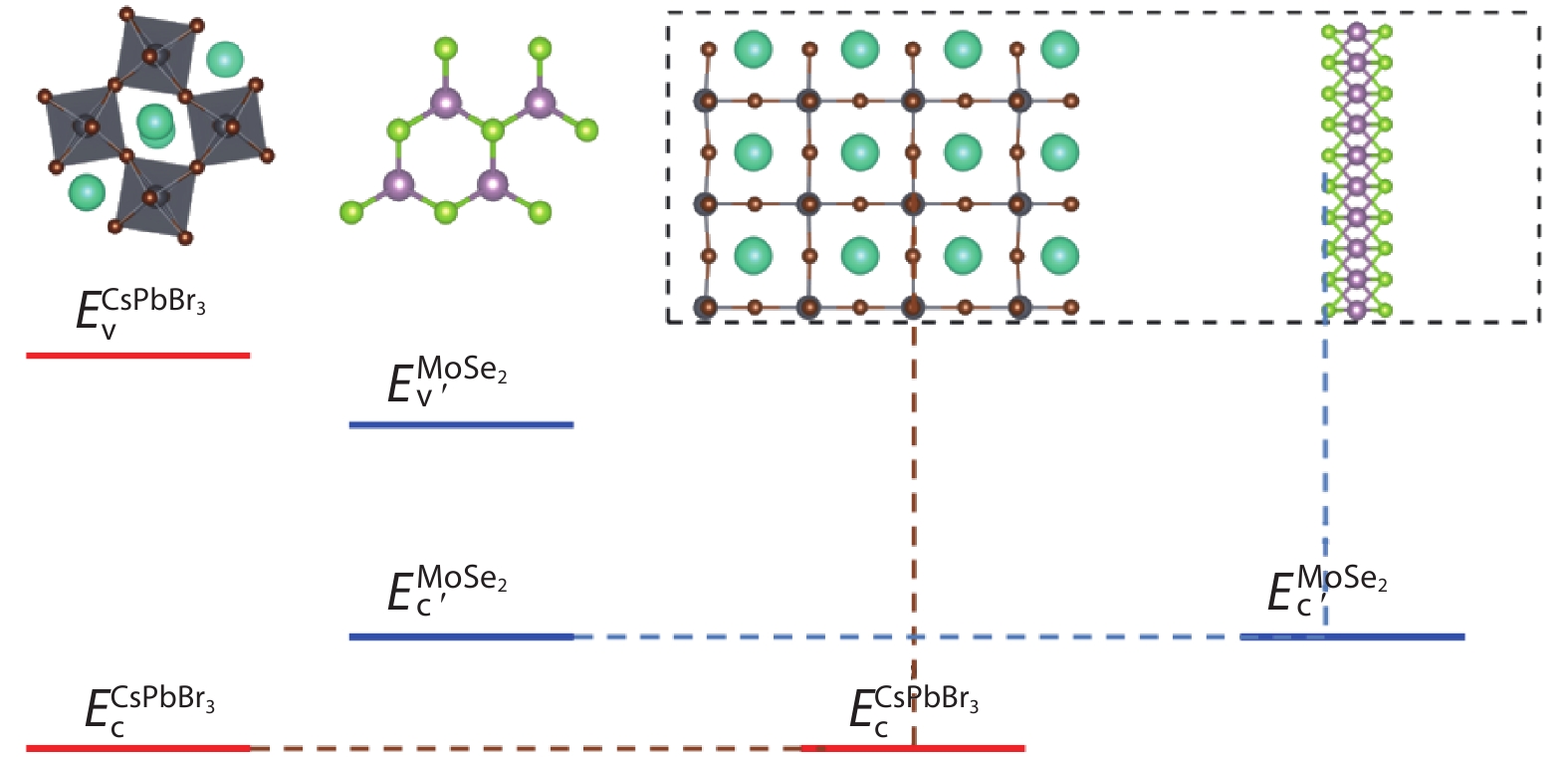
    Fig. 1. (Color online) Schematic procedure to calculate the valence band offsets for heterostructured CsPbBr3/MoSe2. (a) Step I, calculating the energy difference between the VBM and core level in γ-CsPbBr3 and monolayer MoSe2, respectively. (b) Step II, calculating the core levels of each layer in CsPbBr3/MoSe2 superlattice and doing core-level alignment. A superlattice of CsPbBr3/MoSe2 is constructed in (b) to do the core-level alignment.
    (Color online) Band structures of (a) γ-CsPbBr3 and (b) MoSe2 monolayer by using PBE (brown lines) and HSE06 (blue lines) functionals. Band structures with and without SOC are both calculated to explore the influence of SOC on the electronic structures. The VBMs are taken as the reference in all the band structures. All of the band gaps are labeled.
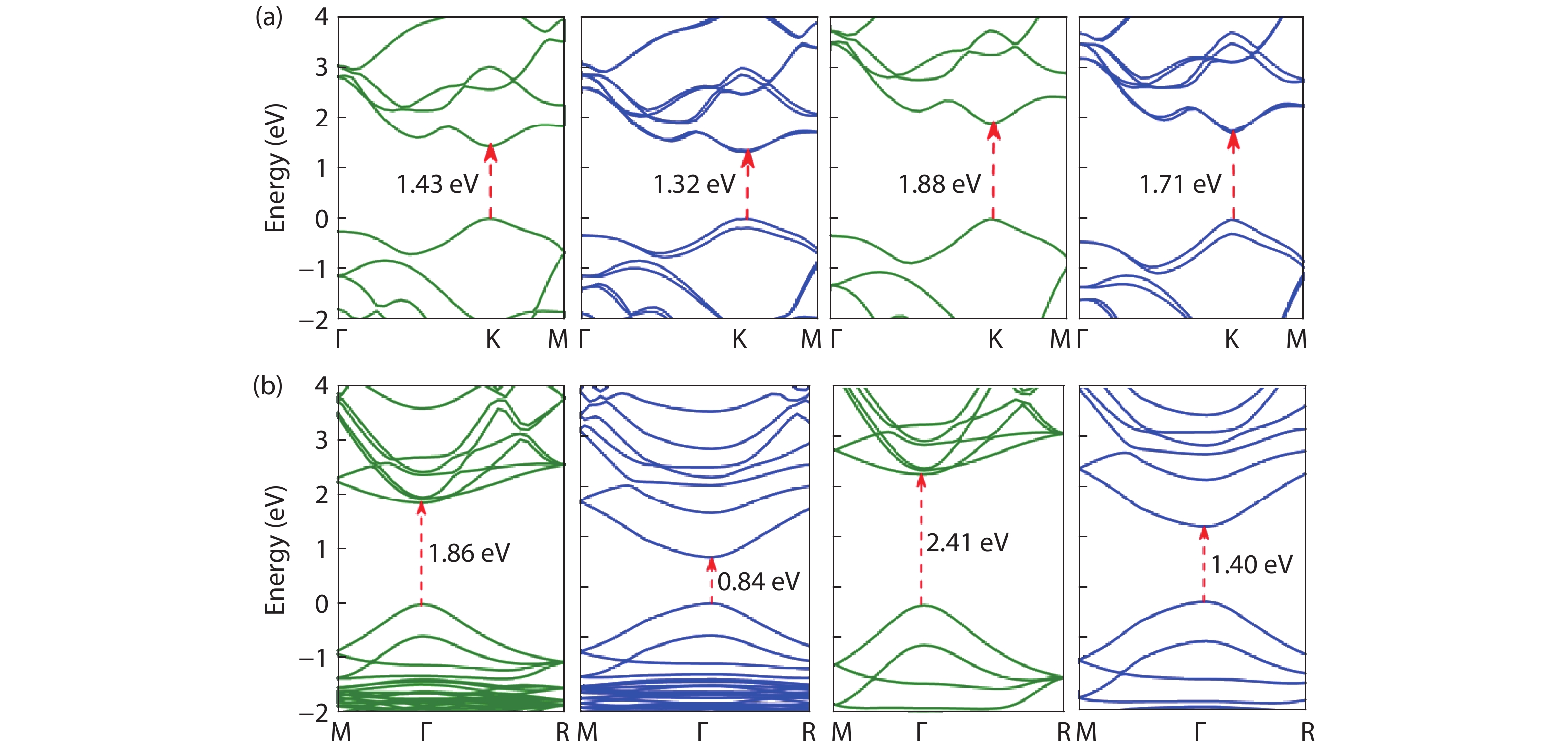
    Fig. 2. (Color online) Band structures of (a) γ-CsPbBr3 and (b) MoSe2 monolayer by using PBE (brown lines) and HSE06 (blue lines) functionals. Band structures with and without SOC are both calculated to explore the influence of SOC on the electronic structures. The VBMs are taken as the reference in all the band structures. All of the band gaps are labeled.
    (Color online) Band alignment of CsPbBr3 and MoSe2 is calculated by using PBE and HSE06 functionals. Conduction and valence band offsets are labeled in black. Red-dashed lines in (d) are the corrected band edges of CsPbBr3 and MoSe2 monolayer with Hatree-Fock exchange percentage of 15% for MoSe2 monolayer and 45% for CsPbBr3. The corrected band gaps are labeled in blue. The conduction and valence band offsets are 0.26 and –0.13 eV, respectively.
    Fig. 3. (Color online) Band alignment of CsPbBr3 and MoSe2 is calculated by using PBE and HSE06 functionals. Conduction and valence band offsets are labeled in black. Red-dashed lines in (d) are the corrected band edges of CsPbBr3 and MoSe2 monolayer with Hatree-Fock exchange percentage of 15% for MoSe2 monolayer and 45% for CsPbBr3. The corrected band gaps are labeled in blue. The conduction and valence band offsets are 0.26 and –0.13 eV, respectively.
    (Color online) The charge difference at the interfaces between MoSe2 monolayer and (a) CsBr-terminated, (b) PbBr-terminated CsPbBr3 slab.
    Fig. 4. (Color online) The charge difference at the interfaces between MoSe2 monolayer and (a) CsBr-terminated, (b) PbBr-terminated CsPbBr3 slab.
    (Color online) The projected band structures of CsPbBr3/MoSe2 heterostructures. (a) Interface between MoSe2 and CsBr-terminated CsPbBr3. (b) Interface between MoSe2 and PbBr-terminated CsPbBr3. The red and blue dots represent the bands dominated by MoSe2 layer and CsPbBr3, respectively.
    Fig. 5. (Color online) The projected band structures of CsPbBr3/MoSe2 heterostructures. (a) Interface between MoSe2 and CsBr-terminated CsPbBr3. (b) Interface between MoSe2 and PbBr-terminated CsPbBr3. The red and blue dots represent the bands dominated by MoSe2 layer and CsPbBr3, respectively.
    Le Huang, Nengjie Huo, Zhaoqiang Zheng, Huafeng Dong, Jingbo Li. Two-dimensional transition metal dichalcogenides for lead halide perovskites-based photodetectors: band alignment investigation for the case of CsPbBr3/MoSe2[J]. Journal of Semiconductors, 2020, 41(5): 052206
    Download Citation