
Le Huang, Nengjie Huo, Zhaoqiang Zheng, Huafeng Dong, Jingbo Li. Two-dimensional transition metal dichalcogenides for lead halide perovskites-based photodetectors: band alignment investigation for the case of CsPbBr3/MoSe2[J]. Journal of Semiconductors, 2020, 41(5): 052206
- Journal of Semiconductors
- Vol. 41, Issue 5, 052206 (2020)
Abstract
1. Introduction
In recent years, lead halide perovskites have attracted enormous attention because of their promising applications in high-performance optoelectronic devices[
Two-dimensional (2D) materials, such as graphene, transition metal dichalcogenides (TMDs) and black phosphorus, and so on, have excellent electronic, optical, and thermal properties[
An exact knowledge of electronic levels is a prerequisite to design optoelectronic devices with good performance and for understanding the device physics[
A unified understanding of the band offsets in perovskites/TMDs is missing. Even the type of their band alignment (type-I or type-II) is under debate. Furthermore, spin-orbital coupling (SOC) has significant influence on the electronic structures of lead halide perovskites (LHPs) and TMDs[
In this work, CsPbBr3 and MoSe2 are taken as prototypes of LHPs and 2D TMDs to investigate the band alignment and interfacial coupling between them. Insights into the SOC effects on the band offsets and interfacial coupling are provided. Our GGA-PBE and HSE06 calculations reveal an intrinsic type-II band alignment between CsPbBr3 and MoSe2 with both the VBM and CBM of MoSe2 monolayer being lower in energy than those of CsPbBr3. The conduction band offset is significantly reduced by the large spin-orbital coupling at the CBM of CsPbBr3. Meanwhile, the valence band offset is reduced by Hartree-Fock exchange interaction. Consequently, an intrinsic type-I alignment is achieved. The type-II band alignment recovers upon CsPbBr3 making contacts with MoSe2 due to the interfacial interaction. Furthermore, no deep defect states are observed in the band gap of CsPbBr3/MoSe2 heterostructures. These results suggest that the performance of CsPbBr3-based photodetectors can be improved by incorporating MoSe2 monolayer.
2. Computational details
We perform our calculations within the projector augmented plane-wave method[
CsPbBr3 in the γphase, which is proved to be the most stable phase[
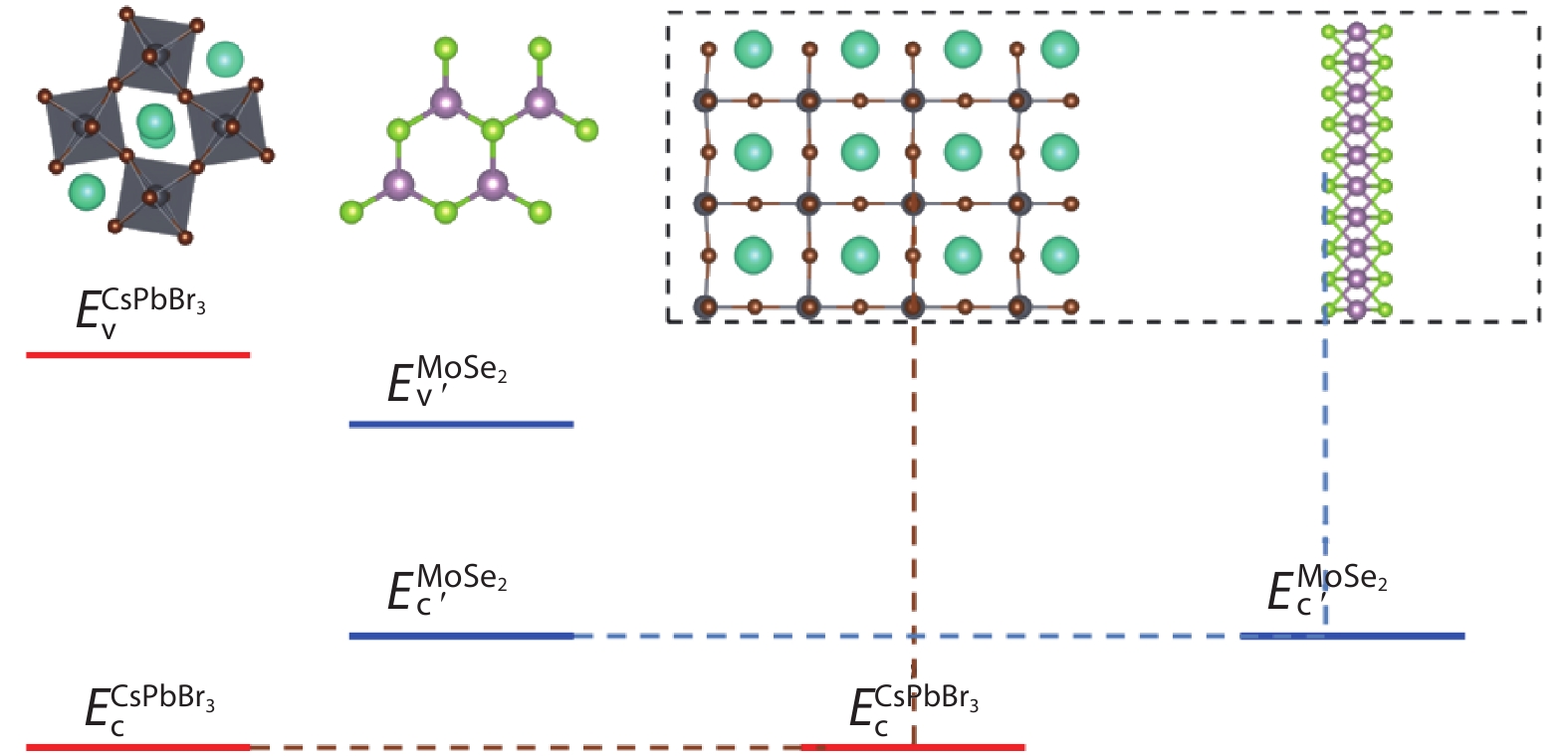
The calculation method for band offsets is illustrated in Fig. 1 and Refs. [53, 54]. Firstly, the energy differences between the core level and the VBM in bulk γ-CsPbBr3 and MoSe2 monolayer are calculated. Then we do the alignment of core levels in CsPbBr3/MoSe2 heterostructure. The valence band offset, ∆Ev, is calculated as
![]()
Figure 1.(Color online) Schematic procedure to calculate the valence band offsets for heterostructured CsPbBr3/MoSe2. (a) Step I, calculating the energy difference between the VBM and core level in
where
Here Br_1s in CsPbBr3 and Se_1s in MoSe2 monolayer are taken as the core levels to do the alignment.
Relativistic first-principles calculations are performed to explore the SOC effect on the electronic structures of CsPbBr3, MoSe2 monolayer and CsPbBr3/MoSe2 interface and its interfacial coupling. To exclude the impact from other factor on the interfacial coupling, we used the heterostructured CsPbBr3/MoSe2 structures that optimized by GGA-PBE functional to explore the SOC effects. The interface coupling is characterized by the binding energy, Eb, between CsPbBr3 slab and MoSe2 monolayer, which is calculated as
where Ehetero,
3. Results and discussion
Fig. 1 shows the crystal structures of γ-CsPbBr3 and monolayer MoSe2, and the schematic alignment procedure to calculate the valence band offsets. The optimized lattice constants of γ-CsPbBr3 are a = b = 8.33 Å, c = 11.91 Å. The lattice constants of monolayer MoSe2 are a = b = 3.33 Å. To do the alignment of the core levels, a superlattice of α-CsPbBr3/MoSe2 is constructed (Fig. 1(b)). During the core level alignment calculations, the lattice constants of α-CsPbBr3 are fixed and strains are applied to the monolayer MoSe2.
At the first step of band offset calculation (Fig. 1(a)), we calculated the electronic structures of γ-CsPbBr3 and MoSe2 monolayer in Fig. 2. MoSe2 monolayer shows a direct band gap of 1.43 eV by GGA-PBE functional and 1.88 eV by HSE06 functional. It has been demonstrated that SOC have significant influence on the VBM at K point in the electronic structures of TMDs. The calculated SOC gap here is 0.18 eV by GGA-PBE functional and 0.28 eV by HSE06 functional. These results agree well with previous works[
![]()
Figure 2.(Color online) Band structures of (a)
In photodetectors based on LHPs/TMDs heterostructures, the band offsets at the interfaces play an important role in their optoelectronic performance. In Figs. 3(a) and 3(b), the band alignment of CsPbBr3/MoSe2 is calculated by using PBE and HSE06 functionals. A type-II band alignment is found for both functionals. Specifically, both the VBM and CBM of MoSe2 are lower than those of CsPbBr3, suggesting that electrons and holes will separate spontaneously with electrons concentrating in MoSe2 layer and holes concentrating in CsPbBr3. Therefore, in optoelectronic devices based on CsPbBr3/MoSe2, the recombination will be reduced and the efficiency can be improved. Comparing the results in Figs. 3(a) and 3(b), larger band gaps are obtained by HSE06 functional than PBE functional. It is found that HSE06 calculation obtains reduced conduction and valence band offsets than PBE results. It should be noted that PBE calculation underestimates the band gaps of CsPbBr3 and monolayer MoSe2 than their experimental values.
![]()
Figure 3.(Color online) Band alignment of CsPbBr3 and MoSe2 is calculated by using PBE and HSE06 functionals. Conduction and valence band offsets are labeled in black. Red-dashed lines in (d) are the corrected band edges of CsPbBr3 and MoSe2 monolayer with Hatree-Fock exchange percentage of 15% for MoSe2 monolayer and 45% for CsPbBr3. The corrected band gaps are labeled in blue. The conduction and valence band offsets are 0.26 and –0.13 eV, respectively.
It has been demonstrated in Fig. 2 that SOC has a significant influence on the band edges of CsPbBr3 and MoSe2 monolayer. Consequently, the band offsets between CsPbBr3 and MoSe2 monolayer can be changed accordingly. When SOC effect included, as shown in Figs. 3(c) and 3(d), our results indicate that the CBM of CsPbBr3 shifts down because of the SOC splitting, resulting in a reduced band gap. Furthermore, the conduction band offset, ∆Ec, is much reduced due to the large SOC splitting at the CBM of CsPbBr3. On the other hand, the influence of SOC on the valence band offset, ∆Ev, is rather weak. Additionally, HSE + SOC calculations indicate a type-I band alignment of CsPbBr3/MoSe2 with band edges of CsPbBr3 encapsulated in that of MoSe2 monolayer. This divergence with experimental results may result from their uncorrected band edges. To reproduce the experimental band gaps of CsPbBr3 and MoSe2 monolayer, we calculated their electronic structures by changing the mixing percentages of Hartree-Fock exchange (15% for MoSe2 monolayer and 45% for CsPbBr3) into the GGA-PBE exchange functional. Then, the MoSe2 monolayer and 45% for CsPbBr3 show corrected band gaps of 1.56 and 1.95 eV, respectively, which are in good consist with experimental values. The corrected band alignment is shown by the dashed lines in Fig. 3(d). Type-I band alignment of CsPbBr3/MoSe2 is maintained after corrections. What makes difference is that the VBM of CsPbBr3 shifts downward to below that of MoSe2 and its CBM shifts upward to higher than that of MoSe2. In this case, both the photon-generated electrons and holes tend to concentrate in the MoSe2 layer. As a result, the performance of photodetectors based on CsPbBr3/MoSe2 can be limited by the electron-hole recombination in MoSe2 layer.
It has been demonstrated that the band offsets of a heterostructure can be modulated by interfacial interaction. In Fig. 4, we explored the interfacial interaction between MoSe2 layer and CsPbBr3 slabs with CsBr and PbBr terminated. Our results show that MoSe2 layer exhibits a stronger binding to PbBr-terminated CsPbBr3 slab (Eb= –1.907 eV per supercell) than to CsBr-terminated one (–1.699 eV). Additionally, SOC effect is revealed to have little influence on the interfacial coupling. (The binding energies become –1.900 and –1.701 eV for corresponding systems above when SOC effect included.) The results of charge difference in Fig. 4 suggest that charge transfer occurs at the CsPbBr3/MoSe2 interface. For both cases, a little negative charge (electrons) transfers from the interfacial metal atoms of CsPbBr3 slab to Se atoms of MoSe2 layer, suggesting a higher CBM of CsPbBr3 slab than MoSe2 monolayer.
![]()
Figure 4.(Color online) The charge difference at the interfaces between MoSe2 monolayer and (a) CsBr-terminated, (b) PbBr-terminated CsPbBr3 slab.
It is known that interfacial charge transfer has influence on the band offsets at interfaces. In Fig. 5, the projected band structures of CsPbBr3/MoSe2 interfaces are calculated to check their band alignments. The bands dominated by CsPbBr3 and MoSe2 are plotted by blue and red dots in Fig. 5. Our results indicate type-II band alignment in both CsPbBr3/MoSe2 interfaces with the CBM and VBM of CsPbBr3 higher than those of MoSe2 layer. Furthermore, there is no deep defect states appear in the band gaps of CsPbBr3/MoSe2 heterostructures, suggesting rather low density of non-radiative recombination center at the interface. This is attributed to the high defect tolerance of CsPbBr3 and no dangling bonds of MoSe2 layer. So, the performance of CsPbBr3 based photodetectors can be improved by inserting a MoSe2 layer to facilitate the separation of photo-generated electrons and holes.
![]()
Figure 5.(Color online) The projected band structures of CsPbBr3/MoSe2 heterostructures. (a) Interface between MoSe2 and CsBr-terminated CsPbBr3. (b) Interface between MoSe2 and PbBr-terminated CsPbBr3. The red and blue dots represent the bands dominated by MoSe2 layer and CsPbBr3, respectively.
It has been demonstrated that if we change the halide atom from Br to I, better light absorption usually can be obtained thanks to reduced band gaps that arise because of the CBM and the VBM approaches the Fermi level[
4. Conclusion
In summary, CsPbBr3 and MoSe2 are taken as prototypes of LHPs and 2D TMDs to investigate the band alignment between them. A type-II band alignment between CsPbBr3 and MoSe2 is manifested by our first-principles calculations by using GGA-PBE and HSE06 functionals. Both the VBM and CBM of MoSe2 monolayer are lower in energy than those of CsPbBr3. The conduction band offset is significantly reduced by the large spin-orbital coupling at the CBM of CsPbBr3, resulting in an intrinsic type-I alignment between them by careful HSE06 + SOC calculations. Upon CsPbBr3 making contacts with MoSe2, the interfacial interaction leads to the upshift of the bands of CsPbBr3 and downshift of the bands of MoSe2, further resulting a type-II band alignment between them. This type-II band alignment suggests that the performance of CsPbBr3-based photodetectors can be improved by incorporating MoSe2 monolayer. Furthermore, the absence of deep defect states at CsPbBr3/MoSe2 interfaces is also beneficial to the better performance of photodetectors based on CsPbBr3/MoSe2 heterostructure. This work not only uncovers the mechanism of improved performance of photodetectors based on CsPbBr3/MoSe2 heterostructures but it also provide guidelines for designing high-efficiency optoelectronic devices based on LHPs/TMDs heterostructures.
Acknowledgements
This work was financially supported by the National Natural Science Foundation of China (Grants No. 11804058, 11674310, 61622406).
References
[1] W Zhang, G E Eperon, H J Snaith. Metal halide perovskites for energy applications. Nat Energy, 1, 16048(2016).
[2] C C Stoumpos, M G Kanatzidis. Halide perovskites: poor man's high-performance semiconductors. Adv Mater, 28, 5778(2016).
[3] Q Lin, A Armin, P L Burn et al. Organohalide perovskites for solar energy conversion. Acc Chem Res, 49, 545(2016).
[4] Y Zhao, K Zhu. Organic–inorganic hybrid lead halide perovskites for optoelectronic and electronic applications. Chem Soc Rev, 45, 655(2016).
[5] J Chen, S Zhou, S Jin et al. Crystal organometal halide perovskites with promising optoelectronic applications. J Mater Chem C, 4, 11(2016).
[6] J Berry, T Buonassisi, D A Egger et al. Hybrid organic–inorganic perovskites (HOIPs): Opportunities and challenges. Adv Mater, 27, 5102(2015).
[7] M M Lee, J Teuscher, T Miyasaka et al. Efficient hybrid solar cells based on meso-superstructured organometal halide perovskites. Science, 338, 643(2012).
[8] S D Stranks, G E Eperon, G Grancini et al. Electron-hole diffusion lengths exceeding 1 micrometer in an organometal trihalide perovskite absorber. Science, 342, 341(2013).
[9] D Liu, T L Kelly. The emergence of perovskite solar cells. Nat Photonics, 8, 133(2014).
[10] D M Jang, K Park, D H Kim et al. Reversible halide exchange reaction of organometal trihalide perovskite colloidal nanocrystals for full-range band gap tuning. Nano Lett, 15, 5191(2015).
[11] R Dong, Y Fang, J Chae et al. High-gain and low-driving-voltage photodetectors based on organolead triiodide perovskites. Adv Mater, 27, 1912(2015).
[12] S A Veldhuis, P P Boix, N Yantara et al. Perovskite materials for light-emitting diodes and lasers. Adv Mater, 28, 6804(2016).
[13] M Liu, M B Johnston, H J Snaith. Efficient planar heterojunction perovskite solar cells by vapour deposition. Nature, 501, 395(2013).
[14] H Zhou, Q Chen, G Li et al. Interface engineering of highly efficient perovskite solar cells. Science, 345, 542(2014).
[15] A Mei, X Li, L Liu et al. A hole-conductor–free, fully printable mesoscopic perovskite solar cell with high stability. Science, 345, 295(2014).
[16] C Zuo, H J Bolink, H Han et al. Advances in perovskite solar cells. Adv Sci, 3, 1500324(2016).
[17] Q Lin, A Armin, P L Burn et al. Filterless narrowband visible photodetectors. Nat Photonics, 9, 687(2015).
[18] Y Fang, Q Dong, Y Shao et al. Highly narrowband perovskite single-crystal photodetectors enabled by surface-charge recombination. Nat Photonics, 9, 679(2015).
[19] S Chen, C Teng, M Zhang et al. A flexible UV-Vis-NIR photodetector based on a perovskite/conjugated-polymer composite. Adv Mater, 28, 5969(2016).
[20] H L Zhu, J Cheng, D Zhang et al. Room-temperature solution-processed niox: PbI2 nanocomposite structures for realizing high-performance perovskite photodetectors. ACS Nano, 10, 6808(2016).
[21] Z K Tan, R S Moghaddam, M L Lai et al. Bright light-emitting diodes based on organometal halide perovskite. Nat Nanotechnol, 9, 687(2014).
[22] H Cho, S H Jeong, M H Park et al. Overcoming the electroluminescence efficiency limitations of perovskite light-emitting diodes. Science, 350, 1222(2015).
[23] S D Stranks, H J Snaith. Metal-halide perovskites for photovoltaic and light-emitting devices. Nat Nanotechnol, 10, 391(2015).
[24] J Yang, B D Siempelkamp, D Liu et al. Investigation of CH3NH3PbI3 degradation rates and mechanisms in controlled humidity environments using in situ techniques. ACS Nano, 9, 1955(2015).
[25] B Hailegnaw, S Kirmayer, E Edri et al. Rain on methylammonium lead iodide based perovskites: possible environmental effects of perovskite solar cells. J Phys Chem Lett, 6, 1543(2015).
[26] Y Y Zhang, S Chen, P Xu et al. Intrinsic instability of the hybrid halide perovskite semiconductor CH3NH3PbI3. Chin Phys Lett, 35, 036104(2018).
[27] K S Novoselov, A K Geim, S V Morozov et al. Two-dimensional gas of massless Dirac fermions in graphene. Nature, 438, 197(2005).
[28] C Lee, X Wei, J W Kysar et al. Measurement of the elastic properties and intrinsic strength of monolayer graphene. Science, 321, 385(2008).
[29] F Bonaccorso, Z Sun, T Hasan et al. Graphene photonics and optoelectronics. Nat Photonics, 4, 611(2010).
[30] Y Sun, Q Wu, G Shi. Graphene based new energy materials. Energy Environ Sci, 4, 1113(2011).
[31] Y Li, L Xu, H Liu et al. Graphdiyne and graphyne: from theoretical predictions to practical construction. Chem Soc Rev, 43, 2572(2014).
[32] F Bonaccorso, L Colombo, G Yu et al. Graphene, related two-dimensional crystals, and hybrid systems for energy conversion and storage. Science, 347, 1246501(2015).
[33] X Song, X Liu, D Yu et al. Boosting two-dimensional MoS2/CsPbBr3 photodetectors via enhanced light absorbance and interfacial carrier separation. ACS Appl Mater Interfaces, 10, 2801(2018).
[34] Y Lee, J Kwon, E Hwang et al. High-performance perovskite-graphene hybrid photodetector. Adv Mater, 27, 41(2015).
[35] Y Wang, R Fullon, M Acerce et al. Solution-processed MoS2/organolead trihalide perovskite photodetectors. Adv Mater, 29, 1603995(2017).
[36] D H Kang, S R Pae, J Shim et al. An ultrahigh-performance photodetector based on a perovskite-transition-metal-dichalcogenide hybrid structure. Adv Mater, 28, 7799(2016).
[37] C Ma, Y Shi, W Hu et al. Heterostructured WS2/CH3NH3PbI3 photoconductors with suppressed dark current and enhanced photodetectivity. Adv Mater, 28, 3683(2016).
[38] P Schulz, E Edri, S Kirmayer et al. Interface energetics in organo-metal halide perovskite-based photovoltaic cells. Energy Environ Sci, 7, 1377(2014).
[39] D Kabra, L P Lu, M H Song et al. Efficient single-layer polymer light-emitting diodes. Adv Mater, 22, 3194(2010).
[40] A Kormányos, V Zólyomi, N D Drummond et al. Spin-orbit coupling, quantum dots, and qubits in monolayer transition metal dichalcogenides. Phys Rev X, 4, 011034(2014).
[41] W J Yin, J H Yang, J Kang et al. Halide perovskite materials for solar cells: a theoretical review. J Mater Chem A, 3, 8926(2015).
[42] P E Blöchl. Projector augmented-wave method. Phys Rev B, 50, 17953(1994).
[43] G Kresse, D Joubert. From ultrasoft pseudopotentials to the projector augmented-wave method. Phys Rev B, 59, 1758(1991).
[44] G Kresse, J Furthmüller. Efficiency of ab-initio total energy calculations for metals and semiconductors using a plane-wave basis set. Comput Mater Sci, 6, 15(1996).
[45] J P Perdew, Y Wang. Density-functional approximation for the correlation energy of the inhomogeneous electron gas. Phys Rev B, 33, 8800(1986).
[46] J P Perdew, K Burke, M Ernzerhof. Generalized gradient approximation made simple. Phys Rev Lett, 77, 3865(1996).
[47] J Heyd, J E Peralta, G E Scuseria et al. Energy band gaps and lattice parameters evaluated with the Heyd-Scuseria-Ernzerhof screened hybrid functional. J Chem Phys, 123, 174101(2005).
[48] J Heyd, G E Scuseria, M Ernzerhof. Hybrid functionals based on a screened Coulomb potential. J Chem Phys, 124, 9906(2006).
[49] S Grimme, J Antony, S Ehrlich et al. A consistent and accurate ab initio parametrization of density functional dispersion correction (DFT-D) for the 94 elements H-Pu. J Chem Phys, 132, 154104(2010).
[50] L Huang, N Huo, Y Li et al. Electric-field tunable band offsets in black phosphorus and MoS2 van der Waals pn heterostructure. J Phys Chem Lett, 6, 2483(2015).
[51] L Huang, L Tao, K Gong et al. Role of defects in enhanced Fermi level pinning at interfaces between metals and transition metal dichalcogenides. Phys Rev B, 96, 205303(2017).
[52] L Huang, M Zhong, H X Deng et al. The Coulomb interaction in van der Waals heterostructures. Sci China: Phys Mech Astron, 62, 37311(2019).
[53] S H Wei, A Zunger. Band offsets and optical bowings of chalcopyrites and Zn-based II–VI alloys. J Appl Phy, 78, 3846(1995).
[54] K T Butler, J M Frost, A Walsh. Band alignment of the hybrid halide perovskites CH3NH3PbCl3, CH3NH3PbBr3 and CH3NH3PbI3. Mater Horizons, 2, 228(2015).
[55] Z Y Zhu, Y C Cheng, U Schwingenschlögl. Giant spin-orbit-induced spin splitting in two-dimensional transition-metal dichalcogenide semiconductors. Phys Rev B, 84, 153402(2011).

Set citation alerts for the article
Please enter your email address
© Copyright 2018-2021 | Chinese Laser Press. All Rights Reserved 沪ICP备15018463号-20