Shanshan Chen, Yongyue Zhang, Xiaorong Hong, Jiafang Li. Technologies and applications of silicon-based micro-optical electromechanical systems: A brief review[J]. Journal of Semiconductors, 2022, 43(8): 081301
Search by keywords or author
- Journal of Semiconductors
- Vol. 43, Issue 8, 081301 (2022)
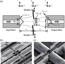
![(a) Schematic diagram of the dual-shutter VOA[21]. (b, c) Fabricated dual-shutter VOA device and a close-up image of the shutter part[21].](/richHtml/jos/2022/43/8/081301/jos_43_8_081301_f1.jpg)
Fig. 1. (a) Schematic diagram of the dual-shutter VOA[21 ]. (b, c) Fabricated dual-shutter VOA device and a close-up image of the shutter part[21 ].
![(Color online) (a) Schematic of two pixels of a DMD chip[19]. (b) An electromagnetically actuated micromirror[39]. (c) An electromagnetically driven 2D MOEMS mirror[37]. (d) A wire bonded 1 × 20 MEMS mirror array[40]. (e) An electrothermal bimorph-actuated MOEMS mirror[41]. (f) A 3D curved micromirror for collimating the output beam of single-mode fibers[42]. (g) Cross section and top view of an electromechanically driven adaptive astigmatic membrane mirror[43]. (h) A micro-deformable mirror architecture[44].](/richHtml/jos/2022/43/8/081301/jos_43_8_081301_f2.jpg)
Fig. 2. (Color online) (a) Schematic of two pixels of a DMD chip[19 ]. (b) An electromagnetically actuated micromirror[39 ]. (c) An electromagnetically driven 2D MOEMS mirror[37 ]. (d) A wire bonded 1 × 20 MEMS mirror array[40 ]. (e) An electrothermal bimorph-actuated MOEMS mirror[41 ]. (f) A 3D curved micromirror for collimating the output beam of single-mode fibers[42 ]. (g) Cross section and top view of an electromechanically driven adaptive astigmatic membrane mirror[43 ]. (h) A micro-deformable mirror architecture[44 ].
Fig. 3. (Color online) (a) SEM image of the fabricated MMI-based spectrometer[52 ]. (b) Multirange spectrometer system[62 ]. (c) Scanning grating MEMS device (dimensions: 9.6 × 5.3 × 0.5 mm3)[58 ]. (d) Schematic of the MOEMS spectrometer[51 ]. (e) SEM image of the scanning diffraction grating[63 ]. (f) Schematic of the FT spectrometer system on a Si optical bench[64 ].
Fig. 4. (Color online) (a) Schematic of the MEMS-actuated matrix switch[67 ]. (b) Schematic of polarization-insensitive Si photonic MEMS switches[70 ]. (c) Schematic representation of a vertically movable silicon photonic MEMS switch[71 ]. Dimensions are not to scale. (d) SEM image showing the grating switch with a stiffener[74 ].

Set citation alerts for the article
Please enter your email address


