Abstract
Micro-optical electromechanical systems (MOEMS) combine the merits of micro-electromechanical systems (MEMS) and micro-optics to enable unique optical functions for a wide range of advanced applications. Using simple external electromechanical control methods, such as electrostatic, magnetic or thermal effects, Si-based MOEMS can achieve precise dynamic optical modulation. In this paper, we will briefly review the technologies and applications of Si-based MOEMS. Their basic working principles, advantages, general materials and micromachining fabrication technologies are introduced concisely, followed by research progress of advanced Si-based MOEMS devices, including micromirrors/micromirror arrays, micro-spectrometers, and optical/photonic switches. Owing to the unique advantages of Si-based MOEMS in spatial light modulation and high-speed signal processing, they have several promising applications in optical communications, digital light processing, and optical sensing. Finally, future research and development prospects of Si-based MOEMS are discussed.Micro-optical electromechanical systems (MOEMS) combine the merits of micro-electromechanical systems (MEMS) and micro-optics to enable unique optical functions for a wide range of advanced applications. Using simple external electromechanical control methods, such as electrostatic, magnetic or thermal effects, Si-based MOEMS can achieve precise dynamic optical modulation. In this paper, we will briefly review the technologies and applications of Si-based MOEMS. Their basic working principles, advantages, general materials and micromachining fabrication technologies are introduced concisely, followed by research progress of advanced Si-based MOEMS devices, including micromirrors/micromirror arrays, micro-spectrometers, and optical/photonic switches. Owing to the unique advantages of Si-based MOEMS in spatial light modulation and high-speed signal processing, they have several promising applications in optical communications, digital light processing, and optical sensing. Finally, future research and development prospects of Si-based MOEMS are discussed.1. Introduction
Following the rapid development of semiconductor technology, the product types of electronic information industry have been greatly expanded, and its integration with traditional industries has aroused great interest. One typical example is micro-electromechanical systems (MEMS)[1]. As a multidisciplinary frontier research field and one of the key directions of national high-tech development, MEMS have flourished since the 1980s[1]. Research on MEMS has further grown[2-4] with the growth of silicon complementary metal oxide semiconductor (CMOS) circuits, giving rise to a wide range of applications in domains such as materials science, energy science, and biomedicine[5-8]. With advances in MEMS, there has been extensive research on micro-optical electromechanical systems (MOEMS), which are MEMS that are used in optical devices. Based on optical theory, MOEMS combine the merits of micro-optical components and MEMS to achieve the integration of light, electricity, and machinery. In MOEMS, the amplitude, wavelength, reflection, diffraction, and other characteristics of a light beam can be tuned using microelectronic and micromechanical devices to achieve the precise control of optical functions. Therefore, owing to their unique advantages and considerable potential in spatial light modulation (SLM) and high-speed signal processing, MOEMS have broad application prospects in the fields of communication, military, aerospace, industry, medicine, and so on, wherein the development of optical communication technology is especially critical[9-13].
With the vigorous renewed rise of industrial transformation, miniaturization, integration, intelligence, versatility, low cost, and high reliability have gradually become important development directions in optical communication and optical sensing. Using highly integrated silicon-based optoelectronics technology, many important components in optical systems (e.g., light emitting and receiving devices, modulators, isolators, attenuators, compensators, optical switches, biological detection chips, and other microelements with customizable functions) can be integrated into a tiny MOEMS to realize versatile optical communication and signal processing chips, enabling the development of next-generation high-speed optical fiber transmission systems and varied photonic integrated devices. The processing technology of versatile Si-based MOEMS is mainly based on mature semiconductor technology because it is compatible with the manufacturing technology of integrated circuit (IC) chips. The material cost for this technology is relatively low, it can integrate well with photoelectric devices, and it has broad market application prospects, such as low-cost thermally tuned external cavity lasers[14], variable optical attenuators (VOAs)[15], optical cross connect[16, 17], and electrooptic modulators[18]. In this review, the technology and recent advances in the applications of Si-based MOEMS are introduced, and their basic working principles and advantages are summarized. We will briefly review their recent applications in micromirrors/micromirror arrays, spectrometers, and optical switches. Finally, some challenges and future trends of Si-based MOEMS are summarized.
2. Working principles and advantages of Si-based MOEMS
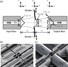
Si-based MOEMS with key dimensions in the micron scale are a research area that combines Si-based MEMS and optics. The relatively mature MEMS technology provides the foundation for realizing the flexible design, large-scale processing, optoelectronic hybrid integration, and precise control of versatile MOEMS. The commercialized digital micromirror device (DMD) projection display chip invented by Texas Instruments (TI) is a typical mature Si-based MOEMS device[19]. It can integrate millions of tiltable mirror-pixels within a few square centimeters and realize SLM by controlling the tilt directions of micromirrors via electrostatic forces; thus, the DMD chip has an important role in several applications, including volumetric displays, holographic data storage, lithography, scientific instrumentation, and medical imaging[20]. The basic working principle of Si-based MOEMS is to use electromechanical control methods (e.g., electrostatic, magnetic, or thermal effects) to realize the precise movement or deformation of internal micro-devices, thereby dynamically influencing the amplitude, phase, and transmission direction of light, finally enabling unique optical functions in the system. Fig. 1 shows a dual-shutter MEMS VOA[21], where the two shutters located between the input and output fibers can move forward and backward, independently driven by a pair of bidirectional comb drives, when a reasonable driving voltage is applied[21].
![(a) Schematic diagram of the dual-shutter VOA[21]. (b, c) Fabricated dual-shutter VOA device and a close-up image of the shutter part[21].](/Images/icon/loading.gif)
Figure 1.(a) Schematic diagram of the dual-shutter VOA[21]. (b, c) Fabricated dual-shutter VOA device and a close-up image of the shutter part[21].
Compared with traditional optoelectronic devices, Si-based MOEMS have several advantages, and thus they comprise an important research field among Si-based optoelectronics technologies. The first advantage is miniaturization and light-weight. MOEMS are compact, with their size varying between a few microns to no more than a few millimeters. Using advanced microelectronics processing technologies, microelements with various functions can be integrated on small Si-based chips while maintaining an extremely light weight, and this directly leads to its high-speed response. The second advantage is low cost and mass producibility. In Si-based MOEMS, the main processing technology uses mature microelectronics manufacturing processes. The raw materials required are Si wafers or Si-on-insulator (SOI) wafers, because of which the cost is much lower than that of III–V group wafer materials. Furthermore, the mature Si-based micromachining technology is compatible with traditional IC processes, making it suitable for mass production. The third advantage is versatility and intelligence. Through the flexible design and precise control of optical elements, MOEMS can achieve a wide range of actions. This deliberate dynamic operation, including the modulation of light wave amplitude or wavelength, transient delay, diffraction, reflection, refraction, and simple spatial self-adaptation, enables specific functions, including light calculation and signal processing. For example, compared with traditional spectrometers that are cumbersome, slow, and expensive[22], the miniaturized MOEMS-based imaging spectrometers are low-cost, high-performance, and reliable.
3. General materials and fabrication techniques
Si is the most commonly used structural material for Si-based MOEMS[23] owing to its excellent mechanical and electrical properties and relatively mature processing technology. According to the microscopic crystal composition, Si materials can be divided into two types: single-crystalline Si and polycrystalline Si. Compared with stainless steel, single-crystalline Si has a higher breaking strength and Knoop hardness, lower density and approximate elastic moduli[23]. The mechanical quality factor of single-crystalline Si is high, and the hysteresis and creep are extremely small, because of which it has excellent mechanical stability[24]. Polycrystalline Si comprises many single-crystalline particles that are arranged and oriented in a disorderly manner, and it is typically fabricated on a substrate via a thin-film process. Its mechanical properties are similar to that of single-crystalline Si, and its electrical properties vary greatly according to the film-forming process[23]. Moreover, Si materials can behave like plasmonic metals with a negative real permittivity[25] when they are doped heavily, and realize various active silicon photonics integrated devices by combining with other active materials[26], making them suitable materials for MOEMS.
MOEMS processing technology is based on MEMS technology, with their main processing technologies borrowed from semiconductor technologies such as lithography, etching, and coating. The most basic Si-based micromachining technology includes bulk micromachining technology and surface micromachining technology[23]. Bulk micromachining technology refers to lithography and chemical etching to remove a part of the matrix or substrate material, obtaining the bulk configuration of required components. It mainly includes wet and dry etching of Si materials. Wet etching of Si can be divided into isotropic etching and anisotropic etching. Isotropic etching is mainly used to generate patterns on Si and to remove damaged Si surfaces. The most commonly used isotropic etching agent for Si is a HNA (hydrofluoric acid, nitric acid, and glacial acetic acid) mixed solution[24]. Anisotropic etching of Si is a popular etching method in Si-based bulk micromachining technology, and it is used to fabricate high-precision 3D structures[23]. Typical anisotropic etching agents include KOH and EPW, among others, and they have different corrosion rates for different crystal planes of Si[24]. Typical dry etching methods are sputter etching, plasma etching, ion beam etching, reactive-ion etching, and deep reactive-ion etching (DRIE). DRIE can achieve high aspect ratios and arbitrary shapes, so it is the most popular dry etching method in MOEMS. The technical characteristics of surface micromachining technology are similar to those of ICs, mainly including the preparation and etching of structural and sacrificial layers. Briefly, sacrificial and structural layers are first deposited on a Si substrate using microelectronic processing technologies such as sputtering, lithography, etching, electroforming, or deposition. The microstructure is then processed into a specific shape, and the sacrificial layer is removed via selective etching to partially separate the structural layer from the Si substrate to obtain a freely movable “mechanical” structure (for motion or sensing), thus realizing the processing of the device. Materials that are commonly used for the structural layer include polysilicon, SiO2, SiN, Al, Ni, and Cu, among others. Materials that are commonly used for the sacrificial layer include phosphosilicate glass, polyimide, polysilicon, Al, and Cu, among others[23]. The thickness of the fabricated microstructures on the surface of Si substrate can be several micrometers. Surface micromachining technology is critical for the fabrication of MOEMS-based devices and most feasible to integrate with IC technology. It is often used to process microhinges, cantilever beams, diaphragms, cavities, and so on[23].
4. Applications of Si-based MOEMS
MOEMS are compatible with IC manufacturing processes, and they are compact, low-cost, and exhibit excellent performance; as a result, they have a wide range of applications in many fields, such as optical communication[27-31] and optical sensing[32-36]. Some examples are micromirror arrays (MMAs) that can achieve effective SLM and optical switches that enable expected changes in the light path. We will next introduce research progress in Si-based MOEMS for micromirrors/MMAs, spectrometers, and optical switches.
4.1. Micromirrors and micromirror arrays
Si-based MOEMS mirrors have many applications, such as machine vision and laser projection[37]. A typical commercial application of MOEMS on new projection display equipment is the DMD realized by TI, which comprises a MOEMS MMA monolithically integrated onto a Si memory chip, and it can be controlled by a digital signal[19]. Fig. 2(a) shows two pixels of the DMD chip, where each aluminum micromirror is 16.2 × 16.2 μm2, and it can be tilted (tilt angles of ±10°) via electrostatic attraction around a pair of thin, compliant torsion hinges[19]. By controlling the digital state (1 or 0) of the underlying static random-access memory cell, the correspondingly tilted micromirror can reflect incident light in one of two distinct directions (±10°) and turn the light on or off at each pixel location on the screen. As early as 1996, digital light processing (DLP) projection displays based on DMD chips were commercialized that could provide bright, stable, seamless, and high-fidelity images[19]. Recently, DMDs have exhibited unique capabilities in implementing multicolor linear structured illumination microscopy (SIM)[38]. Multi-wavelength coherent SIM is regularly achieved using diffraction gratings or liquid crystal on silicon spatial light modulators for fringe projection, but the maximum achievable pattern display rate is limited by physical translation and rotation of the grating or the refresh rate of the spatial light modulator. Brown et al. leveraged a single DMD as a polychromatic diffractive optic for multi-wavelength coherent SIM, providing a new theoretical framework and approach that is cheaper and faster[38]. Besides DMDs, in 2017, Li et al. reported a large-size MEMS-based 2D scanning mirror (diameter = 6.5 mm) driven by electromagnetic force for use in laser projection systems[39]. This can suppress laser speckle and achieve high-power laser illumination for high lumen projection. As shown in Fig. 2(b), a Ni film that can be magnetized in the magnetic field generated by external current coils, was electroplated on the back of a Si wafer to realize the deflection of the micromirror[39]. The efficient electromagnetic drive mode provided the required large-angle driving moment for the micromirror and realized high frequencies, effectively reducing the speckle contrast and generating more aesthetically pleasing images[39]. In 2021, Yu et al. designed a fast-scan MOEMS-based mirror that is also driven by an electromagnetic field[37]. They demonstrated its applications for high-definition laser projection systems[37]. As shown in Fig. 2(c), the electromagnetically driven biaxial scanning micromirror deflects under Lorentz’s force generated by the outer magnetic field and the metal electric coil. Under a driving current of 100 mA, the mechanical deflection angle was ±8.5° along the slow axis at a resonant frequency of 60 Hz, while it was ±12.5° along the fast axis at a resonant frequency of ~37 kHz, which is more than the fast scanning frequency of 27 kHz required to achieve a resolution of 720 P[37]. Thus, laser image projection with 720 P (1280 × 720) resolution at a refreshing frame rate of 60 Hz was realized using the micromirror[37].
Figure 2.(Color online) (a) Schematic of two pixels of a DMD chip[19]. (b) An electromagnetically actuated micromirror[39]. (c) An electromagnetically driven 2D MOEMS mirror[37]. (d) A wire bonded 1 × 20 MEMS mirror array[40]. (e) An electrothermal bimorph-actuated MOEMS mirror[41]. (f) A 3D curved micromirror for collimating the output beam of single-mode fibers[42]. (g) Cross section and top view of an electromechanically driven adaptive astigmatic membrane mirror[43]. (h) A micro-deformable mirror architecture[44].
Compared with electrostatic and electromagnetic actuators, electrothermal bimorphs can achieve greater mechanical displacement at lower driving voltages because of the large strain difference when materials with different thermal expansion coefficients are used[40]. For instance, in 2016, Chen et al. designed and realized an electrothermal actuated 1 × 20 MEMS mirror line array[40]. Its mechanical tilt angle was ±7.8° and ±3.8° along the x- and y-axes, respectively, at a driving voltage of <10 V [40]. As shown in Fig. 2(d), 20 mirrors were arranged with narrow gaps to achieve high fill factors (96%); each mirror plate was supported by four independent lateral-shift-free bimorph actuators to control its 2D tilt. When a voltage was applied to the actuators, the bimorph bent under the action of the Joule heat generated due to the different thermal expansion coefficients of the two layers (Al and SiO2) of the bimorph structure. When four actuators driven differentially were used to control the four corners of the micromirror plates, angular scans along two axes were achieved. In 2021, Ahn et al. reported an electrothermal bimorph-actuated large-area and ultrathin MOEMS mirror (Fig. 2(e))[41]. It provided efficient light-coupling, large scanning area, and high energy efficiency for actuation, and it could overcome the film deformation caused by residual thin-film stresses because of the use of Si rim microstructures, thus maintaining high flatness during actuation[41].
Another type of MOEMS mirror is based on non-planar microsurfaces. The in-plane optical beam collimation is an important performance factor in optical MEMS. It is usually achieved by integrating microlenses in the system[42], which greatly limits the working wavelength range of the system and increases the manufacturing and assembly cost. In 2017, Sabry et al. demonstrated optical fiber light collimation using a Si MEMS 3D curved mirror, as shown in Fig. 2(f)[42]. When the incident beam is in-plane and inclined at 45° with respect to the principal axis, the reflected beam shows a beam-waist ratio of ~4.25 and an ~12 dB reduction in propagation losses[42]. This type of micromirror may potentially replace lensed fibers that are widely used in MOEMS to produce monolithically integrated systems, achieving wider-band spectral responses[42]. In 2021, Kallmann et al. realized an adaptive parabolic cylinder mirror using MEMS technology for the first time, in which only the long axis was deformed parabolically whereas the short axis remained flat[43]. The electromechanically driven adaptive astigmatic membrane mirror system comprises a suspended Si membrane, aluminum counter electrodes, and a bottom fused silica chip, as shown in Fig. 2(g). When a voltage is applied between the Si membrane and the counter electrodes, the Si film exhibits the desired variations in parabolic surface curvature. Adaptive optical micromirror components have several important optical applications such as astronomical instruments. In 2005, Zamkotsian of Laboratoire d’Astrophysique de Marseille predicted that one of the major applications of MOEMS in astronomy is micro-deformable mirrors for adaptive optics because they can provide the key toward achieving small, low-cost, light, and scientifically efficient instruments (Fig. 2(h))[44]. In 2012, Zamkotsian collaborated with Noell of Ecole Polytechnique Fédérale de Lausanne; they used MMAs to achieve next-generation multiobject spectroscopy instruments for space applications[45].
The continuous advances in Si-based MOEMS technology guarantee the realization of various novel micromirrors, and greatly promote the design of micromirrors and MMAs. A variety of MOEMS mirrors are also constantly emerging for use in different fields, such as micro multi-mirrors[46], multilayer Si mirrors[47], rotational MEMS mirrors[48], ultrathin MEMS micromirror[49], and monolithic 3D Si micromirrors[50].
4.2. Micro-spectrometers
In sensing technology, spectroscopy has the advantage of high selectivity owing to the unique “fingerprint” of molecules[51]. Thus, spectroscopy is widely used in various fields, such as agriculture, water quality and forest disaster monitoring, biochemical sensing, and the research and characterization of small biomolecules, tissues, and materials[51]. However, with the increasing requirements of sensing systems, the feasibility of their applications is greatly restricted due to the large size, high power consumption, high cost, and inconvenience for the secondary development of traditional spectroscopic instruments. The fusion of MEMS and integrated photonics (i.e., MOEMS) has efficiently solved the problem. Si-based MOEMS enable the monolithic integration of different spectrometer components, including actuators, micro-mirrors and beam splitters, via a simple lithographic process followed by simultaneously etching such components on Si substrates[52]. Such integration and miniaturization of the spectrometers can significantly reduce the size of the structures as well as cost and power consumption. MOEMS have been used to realize Fourier transform (FT) infrared (IR) spectrometers[53-56], tunable filter spectrometers[57], and diffraction grating based spectrometers[58], and they provide insights for new applications of micro-spectrometers such as healthcare monitoring, gas sensing, food quality control, and industrial applications[52]. For example, hyperspectral IR imagers are essential in applications that require remote identification of complex chemical reagents. Hyperspectral datasets are typically obtained by separating incident light into spectral bands using grating or FT spectrometers[22]. To solve the problems of general spectrometers that are large, cumbersome, slow, and expensive, in 2014 Velicu et al. presented a miniaturized IR imaging spectrometer by coupling a mercury cadmium telluride (HgCdTe)-based IR focal plane array with a MEMS-based Fabry-Perot filter (FPF)[22]. The two membranes were fabricated using bulk micromachining technology. This research demonstrated the viability of designing and fabricating MEMS-based FPFs for the use of rapid hyperspectral detection over a broad wavelength range.
MOEMS spectrometers have considerable application potential in future healthcare and environmental monitoring; Michelson interferometers and scanning gratings are two types of core optical components. MEMS-based Michelson interferometers that use Si interface as a beam splitter have been proposed to realize monolithically integrated on-chip FTIR spectrometers[59]; however, the Si beam splitter exhibited high absorption loss in the visible range and high material dispersion in the near infrared (NIR) range[59]. In 2014, Al-Demerdash et al. realized a novel monolithic MOEMS FT spectrometer that operated over a wide spectral range covering both the IR and visible ranges; it used a hollow multi-mode interference (MMI) splitter/combiner, as shown in Fig. 3(a)[52]. The novel interferometer was fabricated on an SOI wafer using DRIE, and it was compact and could be integrated and manufactured on a large scale at low costs. In 2018, Samir et al. reported a MEMS-based high-resolution FTIR spectrometer for low-cost gas sensing in the NIR range and demonstrated the detection of C2H2 and CO2[60]. The core engine of this spectrometer was a scanning Michelson interferometer built using DRIE on SOI wafers; its working wavelength range was 1300−2500 nm. Similarly, in 2020, Ghonameet al. presented a scanning Michelson interferometer on a Si chip as the core engine, achieving a MEMS-based attenuated total reflection FTIR spectrometer working in the wavelength range of 1.8−6.8μm; they demonstrated its application for obtaining the spectra of different liquid samples. They also investigated the effect of the attenuated total reflection crystal refractive index on the absorption depth, paving the way for various applications in the fields of oil analysis, food safety, and healthcare[61]. In 2021, Salem et al. demonstrated a dual-spectral range MEMS FTIR spectrometer comprising two identical Michelson interferometers working in parallel and monolithically integrated on a single Si chip (Fig. 3(b))[62]. Two different detectors were used to analyze the modulated light in the NIR and mid-infrared (MIR) ranges, respectively, from the two interferometers; the working spectral range was 1.4−4.6 µm and the spectral resolution was ~31.5 cm−1. The MOEMS spectrometer can be adopted for several large-scale spectral sensing applications[62].
Figure 3.(Color online) (a) SEM image of the fabricated MMI-based spectrometer[52]. (b) Multirange spectrometer system[62]. (c) Scanning grating MEMS device (dimensions: 9.6 × 5.3 × 0.5 mm3)[58]. (d) Schematic of the MOEMS spectrometer[51]. (e) SEM image of the scanning diffraction grating[63]. (f) Schematic of the FT spectrometer system on a Si optical bench[64].
NIR is an interesting electromagnetic spectrum for new mobile spectroscopic applications[58]. MOEMS can be used to realize various scanning grating NIR spectrometers. In 2016, Pügner et al. designed a new miniaturized scanning grating spectrometer for NIR spectroscopy (Fig. 3(c)) to meet the requirements for mobile applications, including spectral range, resolution, overall size, robustness, and cost[58]. The spectrometer was compact (volume = 2.1 cm3) and could be integrated into a mobile phone with a spectral range of 950 to 1900 nm at a resolution of 10 nm[58]. In 2020, Ahdab et al. fabricated a tunable MOEMS spectrometer on a thick Si photonic platform in a monochromator setup (Fig. 3(d))[51]. It comprised a concave grating fabricated in a planar waveguide connected to a rotational electrostatic actuator, which enabled angular tuning of the grating. The spectrometer covered a broad working wavelength range and required only a single photodetector to acquire the spectrum[51]. In 2021, Farrugia et al. designed and fabricated a novel MEMS scanning grating to develop portable, low-cost IR spectrometers, as shown in Fig. 3(e)[63]. Based on the thermal stress mismatch between the Si device layer and the reflective metal layer, the diffracted beam could be directly realized by scanning the grating[63].
In addition to scanning gratings, other MOEMS components can also be used to realize micro-spectrometers with custom characteristics. Wang et al. reported a compact FT spectrometer system comprising a large-stroke electrothermal MEMS mirror and other optical components integrated on a micromachined Si optical bench with a footprint of 2 × 2 cm2 (Fig. 3(f))[64]. The linear optical path difference generated by the MEMS-based mirror had a scanning range of up to 450 µm, and the inclination of the mirror plate decreased to < ±0.002° owing to the use of a new open-loop control method [64]. A spectral resolution of 40 cm−1, or 1.1 nm at 532 nm, was achieved[64]. Researchers are consistently developing more methods; for example, Jung Dong et al. reported a Si prism-based NIR spectrometer in 2017[65] and Eltagoury et al. reported an all-Si double-cavity FTIR spectrometer[54].
4.3. Optical/photonic switches
Traditional electricity-centric switches are increasingly unable to meet the needs of high-speed and large-capacity optical communications. In contrast, studies have demonstrated the potential of optical/photonic MEMS switches for applications in large integrated photonic circuits, especially in terms of scalability and power efficiency[66]. In 2005, Wu et al. reported a large-scale Si photonic switch with high port counts and low on-chip losses realized by integrating MEMS actuators with Si photonics (Fig. 4(a))[67]; this switch was fundamentally more scalable than other Si photonic switches[67-69]. The switch employs passive crossbar architecture and MEMS switching mechanisms with very high ON-OFF ratios (>60 dB)[67]. Experimental studies have demonstrated the high performance, low loss, and especially short switching time of these switches, and thus their potential applications in data-intensive computing and reconfigurable networks. The research team reported another 50 × 50 Si photonic MEMS switch with lower polarization dependence in 2018 (Fig. 4(b))[70]. By removing all polarization-dependent elements and using a multi-level waveguide crossbar and MEMS-actuated adiabatic couplers, low polarization-dependent losses (<1 dB) were realized. However, to fully utilize the silicon photonics technology platform to realize various functions of the device, the photonic MEMS switch and other standard components should be integrated into contemporary platform stacks. Recently, Sattariet al. successfully implemented vertically and horizontally movable MEMS components, including optical switches, in the well-established ISIPP50G platform of Interuniversity Microelectronics Centre, Leuven, Belgium[71-73]. Fig. 4(c) shows the vertically movable silicon photonic MEMS switch, which has three suspended directional couplers and six optical ports[71]. Optical/photonic MEMS switches can be applied to waveguide devices as well as to free-space devices. In 2020, Cook et al. reported a novel polysilicon grating switch comprising an optical grating suspended on a moving platform above a waveguide (Fig. 4(d))[74]. These switches differ from other optical waveguide MEMS switches[75, 76] in that they couple into free space, rather than another waveguide[74]. When the switch is “OFF,” the switch is far enough away from the waveguide so that the light propagating in it will not interact with the grating, and when the switch is “ON,” the evanescent field of light is coupled to the grating. Because of this optical design, light can enter the free space at the designed emission angle and numerical aperture.
Figure 4.(Color online) (a) Schematic of the MEMS-actuated matrix switch[67]. (b) Schematic of polarization-insensitive Si photonic MEMS switches[70]. (c) Schematic representation of a vertically movable silicon photonic MEMS switch[71]. Dimensions are not to scale. (d) SEM image showing the grating switch with a stiffener[74].
In addition to the three applications discussed above, Si-based MOEMS devices have many applications in fields such as MOEMS actuators[77] and accelerometers[78], variable optical attenuators[79], spectral sensor heads[80], blazed gratings[81], mass spectrometers[82], and scanners[83, 84]. For example, Sandner et al. proposed a translatory MOEMS actuator with an excellent large stroke driven by electrostatic resonance; it was especially developed for fast optical path length modulation in miniaturized FTIR spectrometers[77]. In 2017, Lu et al. realized an ultrasensitive single-axis out-of-plane MOEMS accelerometer with relatively low cross-axis sensitivity (an order of magnitude less than a conventional accelerometer)[78]. In 2020, Zheng et al. demonstrated a monolithic two-axis forward-view optical scanner comprising an electrothermally driven MEMS mirror and a beam-folding mirror[83]. This compact MOEMS enabled the fabrication of forward-view scanning endoscopic probes with an outer diameter as small as 2.5 mm; such imaging probes can enter the subsegmental bronchi of adult patients[83].
5. Conclusions and perspectives
In summary, we briefly reviewed the technologies and recent applications of Si-based MOEMS. The basic working principle of realizing SLM and mature micromachining technology were introduced, followed by a discussion of research advances of Si-based MOEMS in micromirrors/MMAs, micro-spectrometers, and optical/photonic switches. Si-based MOEMS have unique advantages in SLM and high-speed signal processing; moreover, they are compact, light-weight, low-cost, mass producible, multifunctional, and intelligent. They have several promising applications, such as optical communications, high-density data storage, imaging displays, military photoelectric reconnaissance equipment, early warning and surveillance systems, and aerospace equipment. Research on Si-based MOEMS has grown exponentially; however, their further development faces some challenges with continuously emerging new market demands. Therefore, the research and development of Si-based MOEMS should consider the following aspects. The first aspect is the design principle of diversification. MOEMS technology is multidisciplinary, spanning across domains such as microelectronics, materials science, physics, chemistry, biology, and mechanics. Different environments have clear restrictions on the materials and functions of the systems, such as deep intelligence, miniaturization, low energy consumption and cost, high strain endurance, stability, temperature resistance, long life, facile integration with base materials, implantable base materials, and so on. The second aspect is the combination of various manufacturing technologies, such as wafer manufacturing, packaging, and testing. The integration and packaging technologies of the systems are essential to industrialize MOEMS, and can determine the cost and performance of MOEMS products. These products need to implement multiple functions such as chip protection and external signal interaction simultaneously, and many realistic factors should be considered, such as different manufacturing standards and the need for customization; this can cause packaging and testing to be more challenging, dramatically increasing the cost. The third aspect is the continuous evolution of the compatibility of MOEMS with new technologies and scientific advances. The technological breakthroughs and wide applications of new materials will greatly improve the performance of Si-based MOEMS products and reduce fabrication costs. Both theoretical and immature potential applications in the current stage will become possible based on future emerging science, materials, and techniques. More powerful, multifunctional, and high-performance devices will be explored beyond the current framework, and these will replace the contemporary devices and achieve unprecedented applications.
Acknowledgements
This work is supported by the National Natural Science Foundation of China under Grant No. 61975016, the Science and Technology Project of Guangdong (2020B010190001), Natural Science Foundation of Beijing Municipality (1212013 and Z190006), Beijing Municipal Science & Technology Commission, Administrative Commission of Zhongguancun Science Park No. Z211100004821009, and Cultivation Project for Basic Research and Innovation of Yanshan University No. 2021LGQN021. The authors thank Analysis & Testing Center at Beijing Institute of Technology for assistance.
References
[1] Y Yang, J Wang. The status and application of MEMS technology. Micronanoelectron Technol, 40, 29(2003).
[2] X N Zang, Q Zhou, J Chang et al. Graphene and carbon nanotube (CNT) in MEMS/NEMS applications. Microelectron Eng, 132, 192(2015).
[3] T Kan, A Isozaki, N Kanda et al. Enantiomeric switching of chiral metamaterial for terahertz polarization modulation employing vertically deformable MEMS spirals. Nat Commun, 6, 8422(2015).
[4] E Arbabi, A Arbabi, S M Kamali et al. MEMS-tunable dielectric metasurface lens. Nat Commun, 9, 812(2018).
[5] P Pitchappa, M Manjappa, C P Ho et al. Active control of electromagnetically induced transparency analog in terahertz MEMS metamaterial. Adv Opt Mater, 4, 541(2016).
[6] G Ciuti, M Nardi, P Valdastri et al. HuMOVE: A low-invasive wearable monitoring platform in sexual medicine. Urology, 84, 976(2014).
[7] G Ciuti, N Pateromichelakis, M Sfakiotakis et al. A wireless module for vibratory motor control and inertial sensing in capsule endoscopy. Sens Actuat A, 186, 270(2012).
[8] G Sgandurra, L Bartalena, G Cioni et al. Home-based, early intervention with mechatronic toys for preterm infants at risk of neurodevelopmental disorders (caretoy): A RCT protocol. BMC Pediatr, 14, 268(2014).
[9] W Li, J Ma, S Yang. Applications of MOEMS in optical communication. Shenzhen Univ J, 19, 43(2002).
[10] C T C Nguyen. Microelectromechanical devices for wireless communications. IEEE 11th Annual International Workshop on Micro Electro Mechanical Systems, 1(1998).
[11] Z You, K Gong, J Lu. Development of smallsat technology and its thinking. Sci Technoly Rev, 3, 43(2001).
[12] F Picard, S Ilias, D Asselin et al. MEMS-based flexible reflective analog modulators (FRAM) for projection displays: A technology review and scale-down study. J Phys: Conf Ser, 276, 012182(2011).
[13] Y Li, T Endo, K Hane. Projection type micro-optical encoder based on MEMS technology. Acta Optica Sinica, 8, 1005(2003).
[14] M Finot, M McDonald, B Bettman et al. Thermally tuned external cavity laser with micromachined silicon etalons: Design, process and reliability. 54th Electronic Components and Technology Conference, 818(2004).
[15] C Marxer, P Griss, N F de Rooij. A variable optical attenuator based on silicon micromechanics. IEEE Photonics Technol Lett, 11, 233(1999).
[16] M Kozhevnikov, N R Basavanhally, J D Weld et al. Compact 64 x 64 micromechanical optical cross connect. IEEE Photonics Technol Lett, 15, 993(2003).
[17] X H Ma, G S Kuo. Optical switching technology comparison: Optical MEMS vs. other technologies. IEEE Commun Mag, 41, S16(2003).
[18] W M Green, M J Rooks, L Sekaric et al. Ultra-compact, low RF power, 10 Gb/s silicon Mach-Zehnder modulator. Opt Express, 15, 17106(2007).
[19] L J Hornbeck. The DMDTM projection display chip: A MEMS-based technology. MRS Bull, 26, 325(2001).
[20] D Dudley, W M Duncan, J Slaughter. Emerging digital micromirror device (DMD) applications. Conference on MOEMS Display and Imaging Systems, 14(2003).
[21] X M Zhang, Q W Zhao, A Q Liu et al. Asymmetric tuning schemes of MEMS dual-shutter VOA. J Light Technol, 26, 569(2008).
[22] S Velicu, C Buurma, J D Bergeson et al. Miniaturized imaging spectrometer based on Fabry-Perot MOEMS filters and HgCdTe infrared focal plane arrays. Conference on Image Sensing Technologies - Materials, Devices, Systems, and Applications, 9100, 91000F(2014).
[23] Z Y Zhou, Z L Wang, L W Lin. Microsystems and nanotechnology(2012).
[24] Q Man. Process integration and optimization of silicon substrate MEMS(2021).
[25] M O Faruque, R Al Mahmud, R H Sagor. Heavily doped silicon: A potential replacement of conventional plasmonic metals. J Semicond, 42, 062302(2021).
[26] Y L Yin, J Li, Y Xu et al. Silicon-graphene photonic devices. J Semicond, 39, 061009(2018).
[27] W M Zhu, X M Zhang, A Q Liu et al. A micromachined optical double well for thermo-optic switching via resonant tunneling effect. Appl Phys Lett, 92, 251101(2008).
[28] H Cai, A Q Liu, X M Zhang et al. Tunable dual-wavelength laser constructed by silicon micromachining. Appl Phys Lett, 92, 051113(2008).
[29] C Marxer, M A Grétillat, V P Jaecklin et al. Megahertz opto-mechanical modulator. Sens Actuat A, 52, 46(1996).
[30] O Manzardo, H P Herzig, C R Marxer et al. Miniaturized time-scanning Fourier transform spectrometer based on silicon technology. Opt Lett, 24, 1705(1999).
[31] M C Wu, O Solgaard, J E Ford. Optical MEMS for lightwave communication. J Lightwave Technol, 24, 4433(2006).
[32] D Sarid, D Iams, V Weissenberger et al. Compact scanning-force microscope using a laser diode. Opt Lett, 13, 1057(1988).
[33] P Pliska, W Lukosz. Integrated-optical acoustical sensors. Sens Actuat A, 41, 93(1994).
[34] M C Oh, J W Kim, K J Kim et al. Optical pressure sensors based on vertical directional coupling with flexible polymer waveguides. IEEE Photonics Technol Lett, 21, 501(2009).
[35] X L Zhou, Q X Yu. Wide-range displacement sensor based on fiber-optic fabry–perot interferometer for subnanometer measurement. IEEE Sens J, 11, 1602(2011).
[36] R Waters, C Tally, B Dick et al. Design and analysis of a novel electro-optical MEMS gyroscope for navigation applications. 2010 IEEE Sensors Conference, 1690(2010).
[37] H J Yu, P Zhou, W J Shen. Fast-scan MOEMS mirror for HD laser projection applications. 2021 IEEE 16th International Conference on Nano/Micro Engineered and Molecular Systems, 265(2021).
[38] P T Brown, R Kruithoff, G J Seedorf et al. Multicolor structured illumination microscopy and quantitative control of polychromatic light with a digital micromirror device. Biomed Opt Express, 12, 3700(2021).
[39] F Y Li, P Zhou, T T Wang et al. A large-size MEMS scanning mirror for speckle reduction application. Micromachines, 8, 140(2017).
[40] Q Chen, J L Ding, W Wang et al. A high fill factor 1 × 20 MEMS mirror array based on ISC bimorph structure. 2016 International Conference on Optical MEMS and Nanophotonics (OMN), 1(2016).
[41] M S Ahn, J Jeon, K W Jang et al. Large-area and ultrathin MEMS mirror using silicon micro rim. Micromachines, 12, 754(2021).
[42] Y Sabry, D Khalil, B Saadany et al. In-plane optical beam collimation using a three-dimensional curved MEMS mirror. Micromachines, 8, 134(2017).
[43] U Kallmann, M Lootze, U Mescheder. Simulative and experimental characterization of an adaptive astigmatic membrane mirror. Micromachines, 12, 156(2021).
[44] F Zamkotsian. Moems, micro-optics for astronomical instrumentation. Conference of the NATO-Advanced-Study-Institute on Optics in Astrophysics, 107(2005).
[45] F Zamkotsian, W Noell. MOEMS devices designed and tested for astronomical instrumentation in space. SPIE MOEMS-MEMS. Conference on Reliability, Packaging, Testing, and Characterization of MEMS/MOEMS and Nanodevices XI(2012).
[46] B Wang, Z Z Liang, Y M Kong et al. Design and fabrication of micro multi-mirrors based on silicon for micro-spectrometer. Acta Phys Sin, 59, 907(2010).
[47] H Omran, Y M Sabry, M Sadek et al. Wideband subwavelength deeply etched multilayer silicon mirrors for tunable optical filters and SS-OCT applications. IEEE J Sel Top Quantum Electron, 21, 157(2015).
[48] J Briere, P O Beaulieu, M Saidani et al. Rotational MEMS mirror with latching arm for silicon photonics. Conference on MOEMS and Miniaturized Systems XIV, 9375, 20(2015).
[49] T Takeshita, T Yamashita, N Makimoto et al. Development of ultra-thin MEMS micro mirror device. 2017 19th International Conference on Solid-State Sensors, Actuators and Microsystems, 2143(2017).
[50] A Fawzy, O M El-Ghandour, H F A Hamed. Notice of violation of IEEE publication principles: Optical coupling of 3D silicon micromirrors. 2018 IEEE 13th Annual International Conference on Nano/Micro Engineered and Molecular Systems, 465(2018).
[51] R El Ahdab, S Sharma, F Nabki et al. Wide-band silicon photonic MOEMS spectrometer requiring a single photodetector. Opt Express, 28, 31345(2020).
[52] B M Al-Demerdash, M Medhat, Y M Sabry et al. MMI-based MOEMS FT spectrometer for visible and IR spectral ranges. Conference on MOEMS and Miniaturized Systems XIII, 8977, 195(2014).
[53] I S El-Sayed, Y M Sabry, W E ElZeiny et al. Transformation algorithm and analysis of the Fourier transform spectrometer based on cascaded Fabry–Perot interferometers. Appl Opt, 57, 7225(2018).
[54] Y M Eltagoury, Y M Sabry, D A Khalil. All-silicon double-cavity Fourier-transform infrared spectrometer on-chip. Adv Mater Technol, 4, 1900441(2019).
[55] B Mortada, M Z Erfan, M Medhat et al. Wideband optical MEMS interferometer enabled by multimode interference waveguides. J Lightwave Technol, 34, 2145(2016).
[56] J Y Chai, K Zhang, Y Xue et al. Review of MEMS based Fourier transform spectrometers. Micromachines, 11, 214(2020).
[57] Y M Sabry, Y M Eltagoury, A Shebl et al. In-plane deeply-etched optical MEMS Notch filter with high-speed tunability. J Opt, 17, 125703(2015).
[58] T Pügner, J Knobbe, H Grüger. Near-infrared grating spectrometer for mobile phone applications. Appl Spectrosc, 70, 734(2016).
[59] K Yu, D Lee, U Krishnamoorthy et al. Micromachined Fourier transform spectrometer on silicon optical bench platform. Sens Actuat A, 130/131, 523(2006).
[60] I Samir, Y M Sabry, M Z Erfan et al. MEMS FTIR spectrometer with enhanced resolution for low cost gas sensing in the NIR. Conference on MOEMS and Miniaturized Systems XVII, 10545, 89(2018).
[61] A O Ghoname, Y M Sabry, M Anwar et al. Attenuated total reflection (ATR) MEMS FTIR spectrometer. Conference on MOEMS and Miniaturized Systems XIX, 11293, 170(2020).
[62] A M Salem, Y M Sabry, A Fathy et al. Single MEMS chip enabling dual spectral-range infrared micro-spectrometer with optimal detectors. Adv Mater Technol, 6, 2001013(2021).
[63] R Farrugia, B Portelli, I Grech et al. A concave moems scanning diffraction grating for infrared micro-spectrometer applications. 2021 IEEE 34th International Conference on Micro Electro Mechanical Systems, 783(2021).
[64] W Wang, J P Chen, A S Zivkovic et al. A compact Fourier transform spectrometer on a silicon optical bench with an electrothermal MEMS mirror. J Microelectromechan Syst, 25, 347(2016).
[65] D G Jung, S H Son, S Y Kwon et al. Silicon prism-based NIR spectrometer utilizing MEMS technology. J Sens Sci Technol, 26, 91(2017).
[66] X Tu, C L Song, T Y Huang et al. State of the art and perspectives on silicon photonic switches. Micromachines, 10, 51(2019).
[67] M C Wu, T J Seok, S Han et al. Large-scale, MEMS-actauated silicon photonic switches. 2015 International Conference on Photonics in Switching, 124(2015).
[68] S Han, T J Seok, N Quack et al. Monolithic 50×50 MEMS silicon photonic switches with microsecond response time(2014).
[69] T J Seok, N Quack, S Han et al. 50×50 digital silicon photonic switches with MEMS-actuated adiabatic couplers(2015).
[70] S Han, T J Seok, K Yu et al. Large-scale polarization-insensitive silicon photonic MEMS switches. J Lightwave Technol, 36, 1824(2018).
[71] H Sattari, A Y Takabayashi, P Edinger et al. Low-voltage silicon photonic MEMS switch with vertical actuation. 2021 IEEE 34th International Conference on Micro Electro Mechanical Systems, 298(2021).
[72] P Edinger, C Errando-Herranz, A Y Takabayashi et al. Compact low loss MEMS phase shifters for scalable field-programmable silicon photonics. 2020 Conference on Lasers and Electro-Optics, 1(2020).
[73] A Y Takabayashi, H Sattari, P Edinger et al. Broadband compact single-pole double-throw silicon photonic MEMS switch. J Microelectromechan Syst, 30, 322(2021).
[74] E H Cook, S J Spector, M G Moebius et al. Polysilicon grating switches for LiDAR. J Microelectromechan Syst, 29, 1008(2020).
[75] T J Seok, N Quack, S Han et al. Large-scale broadband digital silicon photonic switches with vertical adiabatic couplers. Optica, 3, 64(2016).
[76] X S Zhang, K Kwon, J Henriksson et al. A 20 × 20 focal plane switch array for optical beam steering. 2020 Conference on Lasers and Electro-Optics, 1(2020).
[77] T Sandner, T Grasshoff, E Gaumont et al. Translatory MOEMS actuator and system integration for miniaturized Fourier transform spectrometers. J Micro-Nanolithogr MEMS MOEMS, 13, 011115(2014).
[78] Q B Lu, J Bai, K W Wang et al. Design, optimization, and realization of a high-performance MOEMS accelerometer from a double-device-layer SOI wafer. J Microelectromechan Syst, 26, 859(2017).
[79] T Graziosi, H Sattari, T J Seok et al. Silicon photonic MEMS variable optical attenuator. Conference on MOEMS and Miniaturized Systems XVII, 10545, 114(2018).
[80] T Yokino, K Kato, A Ui et al. Grating-based ultra-compact SWNIR spectral sensor head developed through MOEMS technology. Conference on MOEMS and Miniaturized Systems XVIII, 10931, 55(2019).
[81] Q Y Nie, Y Y Xie, F Chang. MEMS blazed gratings fabricated using anisotropic etching and oxidation sharpening. AIP Adv, 10, 065216(2020).
[82] P Szyszka, T Grzebyk, M Białas et al. Towars portable MEMS mass spectrometer. 2019 19th International Conference on Micro and Nanotechnology for Power Generation and Energy Conversion Applications, 1(2019).
[83] D Zheng, D K Wang, Y K Yoon et al. A silicon optical bench-based forward-view two-axis scanner for microendoscopy applications. Micromachines, 11, 1051(2020).
[84] D K Wang, S J Koppal, H K Xie. A monolithic forward-view MEMS laser scanner with decoupled raster scanning and enlarged scanning angle for micro LiDAR applications. J Microelectromechan Syst, 29, 996(2020).