Author Affiliations
1School of Electrical and Electronic Engineering, Nanyang Technological University, Singapore 639798, Singapore2Low Energy Electronic Systems (LEES), Singapore-MIT Alliance for Research and Technology, Singapore 138602, Singapore3Department of Materials Science and Engineering, Massachusetts Institute of Technology, Cambridge, Massachusetts 02139, USA4Materials Research Laboratories, Massachusetts Institute of Technology, Cambridge, Massachusetts 02139, USA5Current address: Max Planck Institute of Microstructure Physics, Halle (Saale) 06120, Germany6Current address: Southern University of Science and Technology, Shenzhen 518055, China7e-mail: jmichel@mit.edushow less
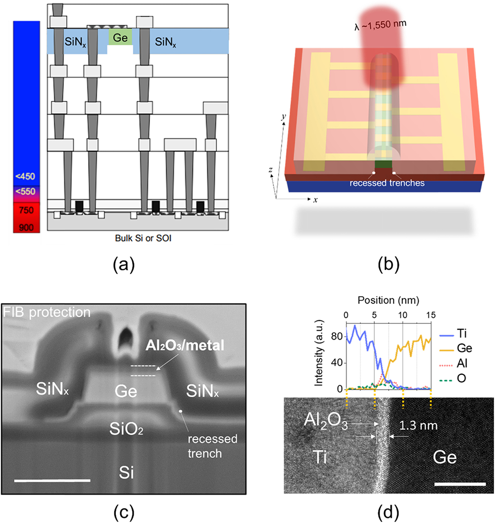
Fig. 1. Recess-strained GOI photodiodes for PICs. (a) Schematic showing the integration of high-quality recess-strained Ge photodiodes with CMOS circuits at back-end-of-line (BEOL). (b) A 3D schematic of a normal-incidence recess SiNx-strained GOI MSM photodiode. The waveguide-shaped Ge is along the ⟨100⟩ direction. Color-coded layers: purple, Si; red, SiO2; green, Ge; gold, contact metal; semitransparent, tensile SiNx. (c) Cross-sectional SEM image of a fabricated device. Scale bar: 1 μm. (d) (Bottom) Cross-sectional TEM image at the Ge/Al2O3/metal interface as shown by the arrow in (c). Scale bar: 10 nm. The corresponding elemental mapping profiles are shown at the top.
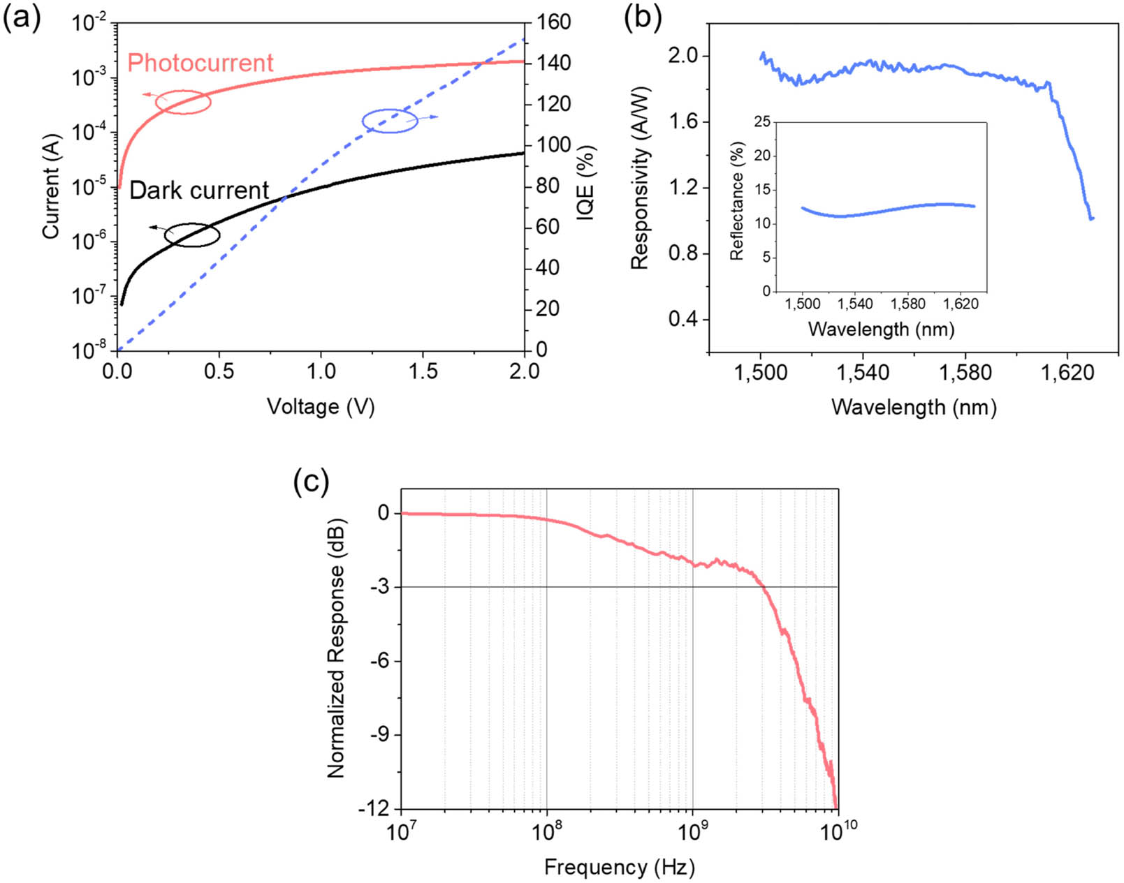
Fig. 2. Characterization of the recess strained GOI MSM photodiodes. (a) Current-voltage (I-V) characteristics of the device without (black) and with (red) an incident power of ∼20 mW at 1550 nm. The corresponding internal quantum efficiency (IQE) is also calculated. (b) Responsivity spectrum of the device from 1500 to 1630 nm. Inset shows the calculated average surface reflectance of the device. (c) Measured frequency response of the device at 2 V.
Fig. 3. Effect of recessed
SiNx stressor on Ge strain and device photocurrent spectra. (a), (b) (i) Schematic GOI structures (a) without and (b) with the
SiNx stressor recessed. The black arrows indicate the spatial tensile strain distributions in Ge. (ii) Corresponding simulated Ge
εxx profiles under 750 MPa tensile stressor using finite element method. (c) Micro-Raman spectra of waveguide GOI testing structure (width: 0.5 μm) with (top) nonrecessed and (bottom) recessed
SiNx stressor. The black dashed line corresponds to the peak LO phonon frequency (
∼300.8 cm−1) of bulk Ge as a stress-free reference. (d) Photocurrent spectra of GOI MSM photodiodes with respect to the use of the nonrecessed and recessed
SiNx stressor. The corresponding Ge absorption coefficients (
α) were also extracted and shown as the
y-axis at right. Absorption coefficients of
In0.53Ga0.47As (data extracted from Ref. [
21]) were also included for reference. Photocurrent roll-off wavelengths: a, 1580 nm; b, 1606 nm; c, 1612 nm.
Fig. 4. Strain, bandgap edge, and absorption coefficient analysis. (a) The simulated Ge εxx [from Figs. 3(a) and 3(b), (ii)] and the Ge bandgap edges [from Fig. 3(d)] agree well with the deformation potential theory. (b) Calculated bandgap edges and α (at 1550 nm) for the GOI photodiodes with 1, 1.2, and 1.5 GPa recessed tensile stressor.
Fig. 5. (a) εxx as a function of GOI waveguide width, with respect to the use of the recessed SiNx stressor with a recessed trench depth of 500 nm. A higher εxx can be achieved with a decreasing width-to-thickness (W/T) ratio. (b) εxx as a function of recessed trench depth. The GOI waveguides are with a width of 0.4 μm and a thickness of 0.2 μm. A higher εxx can be achieved with a deeper recessed trench depth. The results were obtained by the finite element method calculation, as described in Appendix A.1. The SiNx stress is 580 MPa tensile in both cases. The error bars in the plots indicate the εxx variation in the respective GOI waveguides.