
Yiding Lin, Danhao Ma, Kwang Hong Lee, Rui-Tao Wen, Govindo Syaranamual, Lionel C. Kimerling, Chuan Seng Tan, Jurgen Michel. PIC-integrable, uniformly tensile-strained Ge-on-insulator photodiodes enabled by recessed SiNx stressor[J]. Photonics Research, 2021, 9(7): 1255
- Photonics Research
- Vol. 9, Issue 7, 1255 (2021)
Abstract
1. INTRODUCTION
Mechanical strain engineering has been an active research topic for decades to alter the material properties of single-crystalline semiconductors, including electronic bandgaps [1,2], carrier effective mass [3,4], and optical nonlinearity [5,6], for intended electronic and photonic applications. For the bandgap engineering to photonic applications, a substantial strain magnitude with spatially uniform distribution is in most cases essential to the materials of interest. This is to create a consistent bandgap profile with wide tunability and coverage throughout the optical mode span (usually in size), for ideal device and system performance. However, considering feasible complementary metal oxide semiconductor (CMOS) integration for photonic-integrated circuits (PICs), a trade-off can arise between the strain uniformity and the integration compatibility with PICs. Prior studies have extensively employed substrate undercut [7,8], removal [9,10], or layer transfer to flexible substrates [11,12] to facilitate both an optimal strain magnitude and uniformity for the materials of interest. However, this poses challenges of electrical interconnections between Si CMOS circuits and the strained materials. A limited number of reports of opto-electronic devices on these strained materials [13–15] are either complicated in fabrication or remain at a preliminary stage for PIC integration. Additionally, the substrate undercut and removal commonly result in a large device footprint (), which can adversely affect a compact PIC integration. On the other hand, abandoning the substrate engineering inevitably leads to strain nonuniformity with a compromised magnitude due to the bulky substrate constraint [16,17]. Meanwhile, there have been studies using lattice-mismatched hetero-epitaxy for the strain engineering [18,19]. However, the epitaxy usually requires a III-V-based template, which also remains challenging at the current stage for monolithic PIC integration.
In this work, we overcome the dilemma by adopting recessed trenches beside the material structure to be strained, together with the use of sidewall silicon nitride () stressors, to achieve both the strain magnitude enhancement and its uniformity improvement. An illustration of the concept is discussed in Ref. [20]. This method does not require a top stressor and leaves space for device metal contacts. Only mature CMOS fabrication processes (e.g., reactive ion etching) are involved, which is straightforward to realize in PIC integration. The design is essentially different from Ref. [17], which unintentionally had a similar structure, since the stressor was much thinner than the recessed trench, and the strain in the material was thus mainly induced from the top stressor independent of the recessed trench. As a proof of concept, we demonstrate normal-incidence, uniformly 0.56% tensile strained germanium-on-insulator (GOI) metal-semiconductor-metal (MSM) photodiodes using the recessed stressors. A fabricated device exhibits an optical responsivity () of at 1550 nm. The is above 1.0 A/W for wavelength from 1500 to 1625 nm. The photocurrent roll-off is extended by to 1612 nm, where the Ge absorption coefficient reveals a enhancement to . To our knowledge, this is the first batch demonstration of a PIC-integrable uniformly strained photonic device at this strain magnitude. The absorption coefficient is superior to that of across the entire measurement window up to 1630 nm [21]. Compared with the nonrecessed devices, the recessed stressor design resulted in an additional increase in the absorption coefficient across the - and -bands. The significantly enhanced absorption can offer competency over the germanium tin (GeSn) and III-V counterparts for imaging, sensing, and free-space communication PICs (e.g., LiDAR, night vision, and 3D sensing), utilizing the matured foundry processes of deposition and Ge epitaxy.
2. DEVICE DESIGN AND FABRICATION
Figure 1(a) illustrates a cross-sectional schematic of a CMOS-integrated GOI photodiode employing the recessed stressor. The low bonding temperature (300°C) and scalability to different wafer sizes [22,23] facilitate GOI the capability to integrate high-quality Ge at the back-end-of-line (BEOL) on versatile PIC platforms, which is suitable for the above free-space PIC applications. Meanwhile, as seen in the figure, the BEOL integration can save the area used for Ge epitaxy for more Si transistors and consequently a compact integration. Figure 1(b) shows a 3D schematic of the recess tensile-strained GOI MSM photodiode, as the proof-of-concept device for the integration in Fig. 1(a). The detailed fabrication for the 200 mm GOI wafer used in this work is discussed in prior work [22,23]. First, unintentionally doped Ge was epitaxially grown on 200 mm Si (100) substrate via metal-organic chemical vapor deposition. A layer was then deposited on both the epi-Ge and another Si handle wafer using plasma-enhanced chemical vapor deposition (PECVD). Afterward, both wafers were treated by plasma for 15 s to activate the surfaces, followed by deionized water rinsing and spin drying. Immediately after the wafer drying, the two wafers were bonded by contacting the surfaces at room temperature. Post-bonding annealing was performed at 300°C for 3 h to enhance the bonding strength. Finally, the Si wafer used for the Ge epitaxy was removed by grinding and tetramethylammonium hydroxide (TMAH) etching to expose the epi-Ge, which was then planarized by chemical-mechanical polishing.
Sign up for Photonics Research TOC. Get the latest issue of Photonics Research delivered right to you!Sign up now
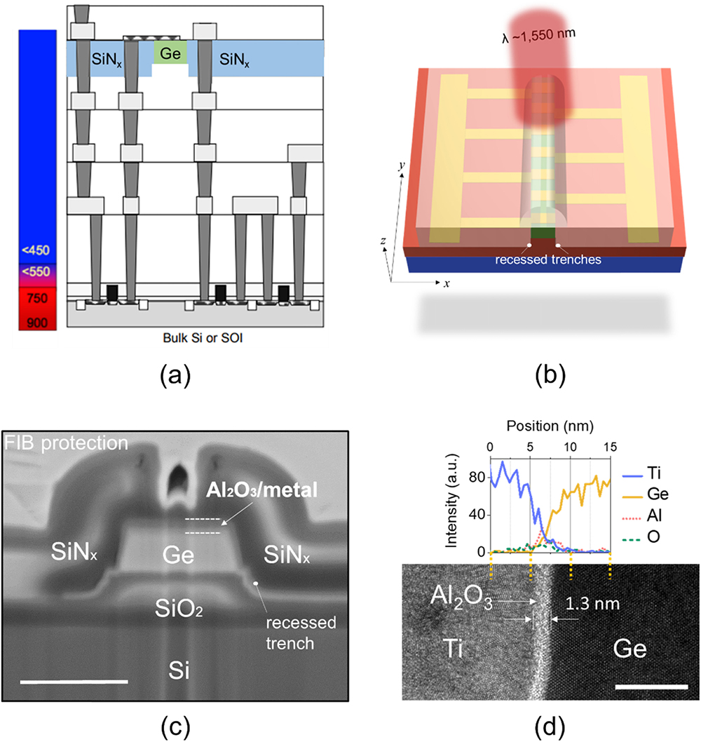
Figure 1.Recess-strained GOI photodiodes for PICs. (a) Schematic showing the integration of high-quality recess-strained Ge photodiodes with CMOS circuits at back-end-of-line (BEOL). (b) A 3D schematic of a normal-incidence recess
The -strained GOI MSM photodiodes employed waveguide-shaped Ge along the direction for the uniform tensile strain along the transverse (-) direction of the waveguide by the recessed stressor [Fig. 1(b)]. The longitudinal (-) direction remains intrinsically strained ( tensile) [24]. The waveguide-shaped design also facilitates high-density arrayed device integration. The devices are with interdigitated metal contacts (Al/TiN/Ti, from top to bottom). There is a nominally 1 nm in between Ti and Ge, deposited by atomic layer deposition, to alleviate the Fermi level pinning. The nominal spacing between adjacent metal fingers is 1 μm. For the ease of fabrication, we fabricated the metal contacts before the stressor deposition. The detailed fabrication steps are described as follows. First, the as-fabricated GOI with a nominal Ge thickness of 400 nm was patterned into strip waveguides (1 μm wide, 36 μm long), using electron-beam lithography (EBL, with ZEP520A resist) followed by chlorine ()-based reactive-ion etching (RIE). Afterward, a second EBL patterning and RIE were performed for the recessed trenches with a nominal depth of 300 nm. After the resist removal, the 1 nm was deposited, followed by the metal contact definition via sputtering and lift-off. Subsequently, the recessed stressor was deposited by PECVD. Optimizing the deposition parameters resulted in a tensile film stress of 750 MPa. To maximize the stressor contact on sidewalls, the thickness of is nominally identical to the total thickness of the Ge waveguide and recessed trench (700 nm). The recessed stressor exerts mechanical tensile stress to both the material to be strained (Ge) and the material underneath (), thus enhancing the strain magnitude at the bottom portion of the Ge close to the and simultaneously improving the strain uniformity [20]. Prior to the deposition, plasma treatment at the surface was carried out for a stronger adhesion of the stressor to the Ge waveguide. The at the top of the Ge waveguide was removed by RIE, as a top tensile could induce undesired compressive strain to the Ge underneath. Finally, the covering the probing metal pads was removed by RIE for the ease of device characterization. For comparison, control devices of -strained GOI MSM photodiodes without the recessed trenches, as well as GOI MSM photodiodes without stressor (50 nm as device passivation), were fabricated. The fabrication steps were kept identical, except for the difference in the stressors for a rigorous comparison.
Figure 1(c) shows a cross-sectional scanning electron microscopy (SEM) image of a fabricated device, prepared by focused-ion beam technique. The Ge width (1.02 μm) and etch depth (243 nm) are as expected close to the nominal values. The stressor adheres well to the Ge and sidewalls without delamination under the tensile stress of 750 MPa. All results indicate reasonably good device fabrication. To further study the metal-Ge Schottky contact, transmission electron microscopy (TEM) characterization was performed. The corresponding image is shown at the bottom of Fig. 1(d). An interlayer of 1.3 nm thickness was observed between Ti and Ge. Elemental mapping at this region by energy dispersive X-ray analysis verifies that the thin interlayer is [Fig. 1(d) top].
3. DEVICE CHARACTERIZATION
The fabricated devices were characterized in terms of their current-voltage () characteristics using a Keithley 2400 source meter unit, with and without normal-incidence illumination, from 293 to 353 K. The optical input was supplied from a TUNICS T100S-HP/CL tunable laser covering 1500–1630 nm. The optical output was coupled into a Corning SMF-28 single-mode silica glass fiber for the illumination. The frequency response of the devices was evaluated by the scattering (S)-parameter measurement via an Agilent N5244A PNA-X network analyzer, with an Agilent N4373D light-wave component analyzer (LCA) as the modulated light source. An RF cable of 40 GHz bandwidth was used. Calibration had been completed before the measurements to exclude the frequency response from the bias-tee, RF cable, and ground-signal-ground probe.
Figure 2(a) shows the room-temperature characteristics of a recess-strained GOI MSM photodiode with and without a 20 mW illumination at 1550 nm. Dark currents of and were observed at biases of 1 and 2 V, respectively, while the illumination leads to prominent photocurrents of and accordingly. To calculate , we assume the fiber tip was placed as close as possible to the device surface without a gap. Considering the mode-field diameter (10.4 μm at 1550 nm) of SMF-28 as the light spot diameter and removing the metal contact area that shielded the illumination, the effective input power on the Ge surface was . Further considering the average surface reflectance of 11.5% [inset of Fig. 2(b)], an of was obtained at 2 V, corresponding to an internal quantum efficiency (IQE) of . The average and IQE among the measured devices are and , respectively. The IQE can be explained by the photoconductive gain [25], as the IQE increases linearly with voltage bias (i.e., electric field). Figure 2(b) shows the responsivity spectrum of the device from 1500 to 1630 nm. This was obtained by performing the spectral scan of the photocurrent of the device and converting the result into a responsivity spectrum, meanwhile taking the surface reflectance into account. A responsivity was observed for wavelength . Temperature-dependent characterization results in a Schottky barrier height of 0.12 eV at 1 V (data not shown), which is lower than the reported value (0.36 eV) [26] and explains the prominent dark current. The dark current can be reduced using a thicker interlayer with lower bandgap (e.g., a-Si:H [27] or Si:C [28]) or negative conduction band offset to Ge (e.g., [29]), without compromising the photocurrent. Alternatively, adopting a structure instead of MSM could also suppress the dark current for the practical CMOS integration. Recently, furnace annealing in ambient oxygen [30] has been demonstrated, which significantly reduced the dark current ( at ) of GOI photodiodes. Figure 2(c) depicts the frequency response of the device. A 3 dB bandwidth of was observed. Although the parasitic capacitance from the metal contact pads is not decoupled, this 3 dB bandwidth performance has been sufficient for most imaging and sensing applications.
![]()
Figure 2.Characterization of the recess strained GOI MSM photodiodes. (a) Current-voltage (
4. STRAIN AND ABSORPTION COEFFICIENT ANALYSIS
The mechanical strain in Ge induced by the stressor, as well as its effect on the material absorption coefficient (), was analyzed. The left figures in Figs. 3(a) and 3(b) show cross-sectional schematics of GOI structures without and with the stressor recessed, respectively, while the right figures show the corresponding simulated strain profiles () in the waveguide-shaped Ge along the transverse (-) direction using the finite element method (Appendix A.1). The Ge waveguide width (1 μm), thickness (400 nm), the recessed trench depth (300 nm), and tensile stress (750 MPa) used in the simulation were identical to the respective nominal values of the fabricated device [Fig. 1(c)]. Structural symmetry was adopted on the and planes at and across the center of the Ge waveguide, respectively. The detailed simulation settings can also be found in our prior report [20]. It can be identified from the color code that the is more uniform in Ge with the use of the recess-type stressor. The corresponding strain magnitude ( tensile) is also higher, especially at the bottom part of Ge where the strain exhibits a enhancement.
![]()
Figure 3.Effect of recessed
To study the effect of stressors on , as described in Section 2, GOI MSM photodiodes (1) without stressor ( passivation) and (2) with nonrecessed stressor were fabricated to compare with the recess-strained device. Figure 3(c) shows the micro-Raman spectra of the strained waveguide GOI test structures without metal contacts. Laser excitation wavelengths of 532 and 785 nm were used for different photon penetration (9 and 89 nm, respectively [31]) depths in Ge for comparison. It can be observed that the Raman spectra reasonably overlap for GOI with the recessed stressor, while only a partial overlap below was seen for that with the nonrecessed stressor. The more wavelength-independent spectra reveal the strain uniformity enhancement with the use of the recessed stressor. Compared with the spectra of the recess-strained structure, the Raman peak broadening for the nonrecessed structure is not due to the deterioration of the Ge crystal quality but to the existence of compressive strain in Ge. It can be further inferred that the compressive strain is located at the bottom of the GOI, which was thus likely induced by the constraint from the bulk -on-Si substrate with the presence of the tensile sidewall stressor. This can also explain the shrinkage of the compressive shoulder [Fig. 2(c), bottom] with the use of the recessed stressor due to the alleviation of the substrate constraint.
Figure 3(d) illustrates the normalized photocurrent spectra of these devices. In contrast with the photocurrent roll-off at for the device without stressor, the roll-off appears at longer wavelengths of 1606 and 1612 nm for the -strained devices with the nonrecessed and recessed stressor, respectively. This indicates both an enhanced and an extended wavelength bandwidth for the -strained GOI devices due to the strain magnitude enhancement. An additional roll-off point was also identified at for the nonrecess strained device. This again demonstrates the strain nonuniformity without the use of the recessed stressor, as shown in the simulation. To correlate the simulated with the roll-off points in the photocurrent spectra, the deformation potential theory [32] was employed to calculate the Ge bandgap edges as a function of , as shown in Fig. 4(a). The calculation includes the -valley-light-hole (-LH) and the -valley-heavy-hole (-HH) bandgap edges. The detailed calculation is discussed in Appendix A.2. It can be seen from the figure that the simulated reasonably match with the observed photocurrent roll-off points. This verifies the validity of the simulation and the actual tensile strain induced in the material. As the Ge layer thickness () is and thus , we can approximate the photocurrent () as , and a photocurrent spectrum of the device can thus be used to extract the Ge absorption coefficient spectrum. We first calculate the direct-band Ge absorption coefficient at 1550 nm using the following relation [33]:
![]()
Figure 4.Strain, bandgap edge, and absorption coefficient analysis. (a) The simulated Ge
The extracted spectra are shown in Fig. 3(d) on the right axis. Compared with the () for the waveguide-Ge without stressor, the () is enhanced by for the recessed -strained Ge at 1612 nm. The for the recess-strained device is superior to that of material () across the - and -bands [21]. The equivalent () for the waveguide Ge without stressor at 1500 nm is extended by 120 nm to 1620 nm for the recessed -strained Ge. All these observations suggest a wider operating wavelength bandwidth for Ge photodiodes, with an expected quantum efficiency superior to that of photodiodes at the - and -bands. This offers potentials for the recess-strained Ge photodiodes for CMOS-compatible imaging, sensing, and communication applications on PICs that the photodiodes may be challenging to achieve. On the other hand, although the Sn incorporation into Ge can also lead to absorption coefficient enhancement [35], state-of-the-art GeSn photodiodes remain challenging to exhibit comparable performance with Ge photodiodes. Further observation of Fig. 3(d) reveals that the use of the recessed trench on the stressor exhibited an additional increase in from 1500 to 1590 nm and a increase from 1590 to 1630 nm, compared with the nonrecess strained device. In addition, we estimate the Ge bandgap edges and with higher stresses of 1.0, 1.2, and 1.5 GPa, using the same simulation and calculation method as above, as shown in Fig. 4(b). The can reach 0.71%, 0.82%, and 1.00% for the stress of 1.0, 1.2, and 1.5 GPa, respectively. The -HH bandgap edge can be extended beyond 1625 nm for the tensile stress , and the correspondingly beyond at 1550 nm. The -HH edge can reach 1645 nm at the stress of 1.5 GPa. Furthermore, a higher can be achieved by using an additional top compressive stressor [36], decreasing the waveguide width-to-thickness (W/T) ratio, or increasing the trench depth (Appendix A.3).
5. CONCLUSION AND OUTLOOK
In conclusion, we have adopted recessed trenches to accommodate sidewall stressors to compromise the trade-off between the mechanical strain uniformity and the integration compatibility to PICs for the material of interest on PICs. As a proof of concept, we demonstrated uniformly 0.56% tensile strained GOI MSM photodiodes using the recessed stressor with a tensile stress of 750 MPa. A fabricated device exhibited a dark current of 41.70 μA and a responsivity of 1.93 A/W (1550 nm) at 2 V, corresponding to an IQE of 155%. The dark current can be reduced by introducing a thicker (narrow bandgap or negative band offset) interlayer or using photodiodes. The bandgap edges revealed from the device photocurrent spectra match well with the simulated via the deformation potential theory. The absorption coefficient calculation showed a Ge absorption coefficient superior to that of throughout the measurement window up to 1630 nm. Meanwhile, the use of the recessed-type stressor exhibited an additional increase in the absorption coefficient. These results facilitate the recess-strained GOI photodiodes for imaging, sensing, and free-space communication (e.g., LiDAR) PIC applications. The recessed stressor design can also be used for strain engineering on other semiconductor materials (e.g., III-V, GeSn).
In addition, it is worth noting that the recessed stressor concept can provide new application insights to existing photonic devices. For instance, a 0.6 GPa tensile electro-absorption (EA) modulator array has recently been demonstrated, exhibiting an operating wavelength range of 95 nm from 1525 to 1620 nm at , where the ratio of extinction ratio (ER)-to-insertion loss (IL) is [37]. This can be useful for high-data-capacity transceiver PICs using dense-wavelength-division multiplexing, due to the wider operating wavelength range compared with that of single Ge EA modulators () [38–40].
Acknowledgment
Acknowledgment. The authors acknowledge the resources from the Nanyang Nanofabrication Center (N2FC) for the device fabrication and Ms. Tina Xin Guo and Dr. Chongyang Liu for the device characterization. Support from Ms. Jin Zhou on the EBL writing is also acknowledged.
APPENDIX A
The finite element method simulation was constructed by mimicking the practical experimental conditions. This was realized by adopting multiple solid mechanics modules in COMSOL Multiphysics, each corresponding to an experimental process, and solving them in sequence according to the experimental procedures. The stress output from the previous module was imported as the initial stress to the subsequent module, and the output from the last module was converted to the final mechanical strain. All materials were set as linear elastic.
The modelling first followed the thermal budget during the GOI fabrication, consisting of the Ge-on-Si epitaxy at 600°C, followed by the direct wafer bonding and post-bonding annealing at 300°C, and finally cooling down to room temperature (300?K). The subsequent GOI patterning and stressor deposition were without temperature variation. An intrinsic stress was set in the . Geometrical symmetry was applied penetrating the structure via the and planes [Figs.?
Deformation potential theory [
Considering the coupling with the spin-orbit split-off (SO) band, Ge -valley conduction-band-light-hole bandgap and conduction-band-heavy-hole bandgap can be expressed as follows, respectively:
Figure?
![]()
Figure 5.(a)
References
[1] M. J. Süess, R. Geiger, R. A. Minamisawa, G. Schiefler, J. Frigerio, D. Chrastina, G. Isella, R. Spolenak, J. Faist, H. Sigg. Analysis of enhanced light emission from highly strained germanium microbridges. Nat. Photonics, 7, 466-472(2013).
[2] R. Rafael, C.-G. Andrés, C. Emmanuele, G. Francisco. Strain engineering in semiconducting two-dimensional crystals. J. Phys. Condens. Matter, 27, 313201(2015).
[3] A. R. Adams. Band-structure engineering for low-threshold high-efficiency semiconductor lasers. Electron. Lett., 22, 249-250(1986).
[4] M. L. Lee, E. A. Fitzgerald, M. T. Bulsara, M. T. Currie, A. Lochtefeld. Strained Si, SiGe, and Ge channels for high-mobility metal-oxide-semiconductor field-effect transistors. J. Appl. Phys., 97, 011101(2004).
[5] R. S. Jacobsen, K. N. Andersen, P. I. Borel, J. Fage-Pedersen, L. H. Frandsen, O. Hansen, M. Kristensen, A. V. Lavrinenko, G. Moulin, H. Ou, C. Peucheret, B. Zsigri, A. Bjarklev. Strained silicon as a new electro-optic material. Nature, 441, 199-202(2006).
[6] M. Cazzanelli, F. Bianco, E. Borga, G. Pucker, M. Ghulinyan, E. Degoli, E. Luppi, V. Véniard, S. Ossicini, D. Modotto, S. Wabnitz, R. Pierobon, L. Pavesi. Second-harmonic generation in silicon waveguides strained by silicon nitride. Nat. Mater., 11, 148-154(2011).
[7] A. Elbaz, D. Buca, N. von den Driesch, K. Pantzas, G. Patriarche, N. Zerounian, E. Herth, X. Checoury, S. Sauvage, I. Sagnes, A. Foti, R. Ossikovski, J.-M. Hartmann, F. Boeuf, Z. Ikonic, P. Boucaud, D. Grützmacher, M. El Kurdi. Ultra-low-threshold continuous-wave and pulsed lasing in tensile-strained GeSn alloys. Nat. Photonics, 14, 375-382(2020).
[8] M. El Kurdi, M. Prost, A. Ghrib, S. Sauvage, X. Checoury, G. Beaudoin, I. Sagnes, G. Picardi, R. Ossikovski, P. Boucaud. Direct band gap germanium microdisks obtained with silicon nitride stressor layers. ACS Photon., 3, 443-448(2016).
[9] F. T. Armand Pilon, A. Lyasota, Y. M. Niquet, V. Reboud, V. Calvo, N. Pauc, J. Widiez, C. Bonzon, J. M. Hartmann, A. Chelnokov, J. Faist, H. Sigg. Lasing in strained germanium microbridges. Nat. Commun., 10, 2724(2019).
[10] A. Gassenq, K. Guilloy, G. Osvaldo Dias, N. Pauc, D. Rouchon, J. M. Hartmann, J. Widiez, S. Tardif, F. Rieutord, J. Escalante, I. Duchemin, Y. M. Niquet, R. Geiger, T. Zabel, H. Sigg, J. Faist, A. Chelnokov, V. Reboud, V. Calvo. 1.9% bi-axial tensile strain in thick germanium suspended membranes fabricated in optical germanium-on-insulator substrates for laser applications. Appl. Phys. Lett., 107, 191904(2015).
[11] J.-H. Seo, E. Swinnich, Y.-Y. Zhang, M. Kim. Low dimensional freestanding semiconductors for flexible optoelectronics: materials, synthesis, process, and applications. Mater. Res. Lett., 8, 123-144(2020).
[12] S. An, S. Wu, C. S. Tan, G.-E. Chang, X. Gong, M. Kim. Modulation of light absorption in flexible GeSn metal–semiconductor–metal photodetectors by mechanical bending. J. Mater. Chem. C, 8, 13557-13562(2020).
[13] J. Jiang, M. Xue, C.-Y. Lu, C. S. Fenrich, M. Morea, K. Zang, J. Gao, M. Cheng, Y. Zhang, T. I. Kamins, J. S. Harris, J. Sun. Strain-induced enhancement of electroluminescence from highly strained germanium light-emitting diodes. ACS Photon., 6, 915-923(2019).
[14] D. Nam, D. Sukhdeo, A. Roy, K. Balram, S.-L. Cheng, K. C.-Y. Huang, Z. Yuan, M. Brongersma, Y. Nishi, D. Miller, K. Saraswat. Strained germanium thin film membrane on silicon substrate for optoelectronics. Opt. Express, 19, 25866-25872(2011).
[15] D. Nam, D. Sukhdeo, S.-L. Cheng, A. Roy, K. C.-Y. Huang, M. Brongersma, Y. Nishi, K. Saraswat. Electroluminescence from strained germanium membranes and implications for an efficient Si-compatible laser. Appl. Phys. Lett., 100, 131112(2012).
[16] G. Capellini, C. Reich, S. Guha, Y. Yamamoto, M. Lisker, M. Virgilio, A. Ghrib, M. El Kurdi, P. Boucaud, B. Tillack, T. Schroeder. Tensile Ge microstructures for lasing fabricated by means of a silicon complementary metal-oxide-semiconductor process. Opt. Express, 22, 399-410(2014).
[17] A. Ghrib, M. de Kersauson, M. El Kurdi, R. Jakomin, G. Beaudoin, S. Sauvage, G. Fishman, G. Ndong, M. Chaigneau, R. Ossikovski, I. Sagnes, P. Boucaud. Control of tensile strain in germanium waveguides through silicon nitride layers. Appl. Phys. Lett., 100, 201104(2012).
[18] M. de Kersauson, M. Prost, A. Ghrib, M. El Kurdi, S. Sauvage, G. Beaudoin, L. Largeau, O. Mauguin, R. Jakomin, I. Sagnes, G. Ndong, M. Chaigneau, R. Ossikovski, P. Boucaud. Effect of increasing thickness on tensile-strained germanium grown on InGaAs buffer layers. J. Appl. Phys., 113, 183508(2013).
[19] Y. Bai, K. E. Lee, C. Cheng, M. L. Lee, E. A. Fitzgerald. Growth of highly tensile-strained Ge on relaxed In
[20] Y. Lin, D. Ma, K. H. Lee, J. Michel, C. S. Tan. A self-aligned dry etching method for mechanical strain enhancement of germanium and its uniformity improvement for photonic applications. Proc. SPIE, 10537, 1053704(2018).
[21] O. I. Dosunmu, D. D. Cannon, M. K. Emsley, B. Ghyselen, J. Liu, L. C. Kimerling, M. S. Unlu. Resonant cavity enhanced Ge photodetectors for 1550 nm operation on reflecting Si substrates. IEEE J. Sel. Top. Quantum Electron., 10, 694-701(2004).
[22] K. H. Lee, S. Bao, G. Y. Chong, Y. H. Tan, E. A. Fitzgerald, C. S. Tan. Fabrication and characterization of germanium-on-insulator through epitaxy, bonding, and layer transfer. J. Appl. Phys., 116, 103506(2014).
[23] Y. Lin, K. H. Lee, S. Bao, X. Guo, H. Wang, J. Michel, C. S. Tan. High-efficiency normal-incidence vertical p-i-n photodetectors on a germanium-on-insulator platform. Photon. Res., 5, 702-709(2017).
[24] Y. Lin, D. Ma, K. H. Lee, S. Bao, J. Michel, C. S. Tan. Extension of Germanium-on-insulator optical absorption edge using CMOS-compatible silicon nitride stressor. Conference on Lasers and Electro-Optics Pacific Rim (CLEO-PR), 1-5(2017).
[25] S. Sze. Semiconductor Devices: Physics and Technology, 311-313(2002).
[26] B. S. Pearson, L. C. Kimerling, J. Michel. Germanium photodetectors on amorphous substrates for electronic-photonic integration. IEEE 13th International Conference on Group IV Photonics (GFP), 20-21(2016).
[27] G. Dushaq, A. Nayfeh, M. Rasras. Metal-germanium-metal photodetector grown on silicon using low temperature RF-PECVD. Opt. Express, 25, 32110-32119(2017).
[28] K.-W. Ang, S. Zhu, M. Yu, G.-Q. Lo, D.-L. Kwong. High-performance waveguided Ge-on-SOI metal–semiconductor–metal photodetectors with novel silicon–carbon (Si:C) Schottky barrier enhancement layer. IEEE Photon. Technol. Lett., 20, 754-756(2008).
[29] J. H. Nam. Monolithic integration of germanium-on-insulator platform on silicon substrate and its applications to devices(2016).
[30] Y. Lin, B. Son, K. H. Lee, J. Michel, C. S. Tan. Sub-mA/cm2 dark current density, buffer-less germanium (Ge) photodiodes on a 200-mm Ge-on-insulator substrate. IEEE Trans. Electron Devices, 68, 1730-1737(2021).
[31] W. S. Yoo, T. Ueda, T. Ishigaki, H. Nishigaki, N. Hasuike, H. Harima, M. Yoshimoto, C. S. Tan. Detection of Ge and Si intermixing in Ge/Si using multiwavelength micro-Raman spectroscopy. ECS Trans., 64, 79-88(2014).
[32] C. G. Van de Walle. Band lineups and deformation potentials in the model-solid theory. Phys. Rev. B, 39, 1871-1883(1989).
[33] J. Liu, X. Sun, D. Pan, X. Wang, L. C. Kimerling, T. L. Koch, J. Michel. Tensile-strained, n-type Ge as a gain medium for monolithic laser integration on Si. Opt. Express, 15, 11272-11277(2007).
[34] A. Frova, P. Handler. Franz-Keldysh effect in the space-charge region of a germanium p−n junction. Phys. Rev., 137, A1857-A1861(1965).
[35] K. Ye, W. Zhang, M. Oehme, M. Schmid, M. Gollhofer, K. Kostecki, D. Widmann, R. Körner, E. Kasper, J. Schulze. Absorption coefficients of GeSn extracted from PIN photodetector response. Solid-State Electron., 110, 71-75(2015).
[36] X. Li, Z. Li, S. Li, L. Chrostowski, G. Xia. Design considerations of biaxially tensile-strained germanium-on-silicon lasers. Semicond. Sci. Technol., 31, 065015(2016).
[37] D. Ma. Ge and GeSi electroabsorption modulator arrays via strain and composition engineering(2020).
[38] D. Feng, W. Qian, H. Liang, C.-C. Kung, Z. Zhou, Z. Li, J. S. Levy, R. Shafiiha, J. Fong, B. Jonathan Luff, M. Asghari. High-speed GeSi electroabsorption modulator on the SOI waveguide platform. IEEE J. Sel. Top. Quantum Electron., 19, 64-73(2013).
[39] N.-N. Feng, D. Feng, S. Liao, X. Wang, P. Dong, H. Liang, C.-C. Kung, W. Qian, J. Fong, R. Shafiiha, Y. Luo, J. Cunningham, A. V. Krishnamoorthy, M. Asghari. 30 GHz Ge electro-absorption modulator integrated with 3 μm silicon-on-insulator waveguide. Opt. Express, 19, 7062-7067(2011).
[40] S. A. Srinivasan, M. Pantouvaki, S. Gupta, H. T. Chen, P. Verheyen, G. Lepage, G. Roelkens, K. Saraswat, D. V. Thourhout, P. Absil, J. V. Campenhout. 56 Gb/s germanium waveguide electro-absorption modulator. J. Lightwave Technol., 34, 419-424(2016).
[41] S. L. Chuang. Physics of Photonic Devices, 80(2012).
[42] J. Liu, D. D. Cannon, K. Wada, Y. Ishikawa, D. T. Danielson, S. Jongthammanurak, J. Michel, L. C. Kimerling. Deformation potential constants of biaxially tensile stressed Ge epitaxial films on Si(100). Phys. Rev. B, 70, 155309(2004).

Set citation alerts for the article
Please enter your email address
© Copyright 2018-2021 | Chinese Laser Press. All Rights Reserved 沪ICP备15018463号-20