• Journal of Semiconductors
  • Vol. 40, Issue 9, 092002 (2019)
Shuaiqin Wu1、2, Guangjian Wu1, Xudong Wang1, Yan Chen1, Tie Lin1、2, Hong Shen1、2, Weida Hu1、2, Xiangjian Meng1、2, Jianlu Wang1、2, and Junhao Chu1、2
Author Affiliations
  • 1State Key Laboratory of Infrared Physics, Shanghai Institute of Technical Physics, Chinese Academy of Sciences, Shanghai 200083, China
  • 2University of Chinese Academy of Sciences, Beijing 100049, China
  • show less
    DOI: 10.1088/1674-4926/40/9/092002 Cite this Article
    Shuaiqin Wu, Guangjian Wu, Xudong Wang, Yan Chen, Tie Lin, Hong Shen, Weida Hu, Xiangjian Meng, Jianlu Wang, Junhao Chu. A gate-free MoS2 phototransistor assisted by ferroelectrics[J]. Journal of Semiconductors, 2019, 40(9): 092002 Copy Citation Text show less
    (Color online) Ferroelectric polarization switching by PFM for 50 nm-thick P(VDF-TrFE) film. (a) Schematic of the operation for P(VDF-TrFE) polarization switching with PFM probe appling a positive or negative voltage. (b) The PFM amplitude (red) and phase (black) hysteresis loops during the switching process, scale bar is 10 μm. (c) Amplitude signal and (d) phase signal of the P(VDF-TrFE) film after writing half-to-half rectangle patterns with reversed DC bias, scale bar is 10 μm.
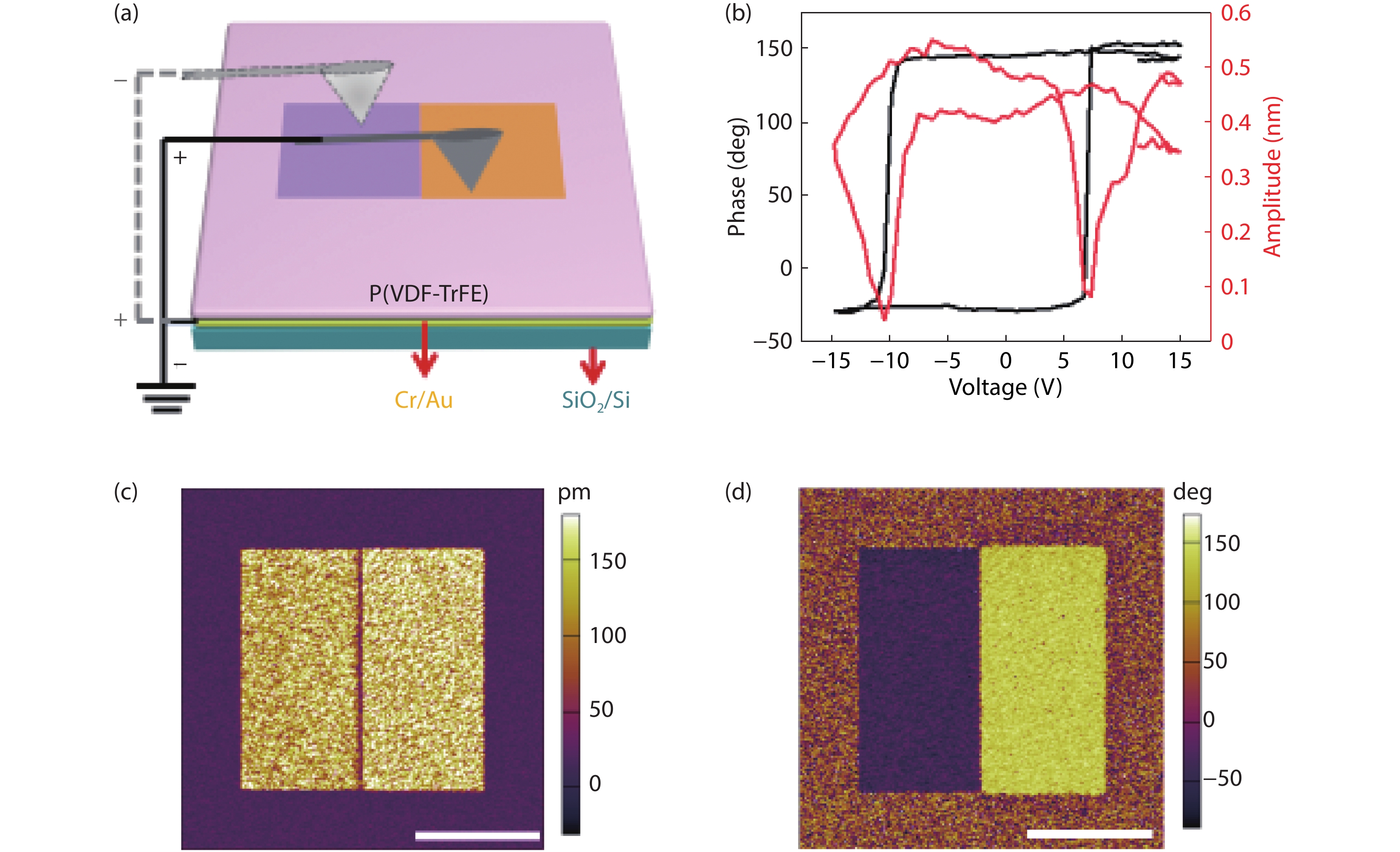
    Fig. 1. (Color online) Ferroelectric polarization switching by PFM for 50 nm-thick P(VDF-TrFE) film. (a) Schematic of the operation for P(VDF-TrFE) polarization switching with PFM probe appling a positive or negative voltage. (b) The PFM amplitude (red) and phase (black) hysteresis loops during the switching process, scale bar is 10 μm. (c) Amplitude signal and (d) phase signal of the P(VDF-TrFE) film after writing half-to-half rectangle patterns with reversed DC bias, scale bar is 10 μm.
    (Color online) Structure illustration of the gate-free MoS2 photodetector. (a) A 3D schematic of the device structure. (b) The optical image of the device, which includes a 3.5 nm MoS2 and Cr/Au source and drain electrodes covered by 50 nm-thick P(VDF-TrFE) film, scale bar is 10 μm. (c) The PFM phase image of the device (red square part in (b)), two polarization states of Pdown and Pup represent the opposite direction of the electric dipole moment in different parts (orange and black), scale bar is 3 μm. (d) Phase profile extracted along the white dashed line in (c), which demonstrated that the MoS2 in the channel has a 180° phase difference with the other part.
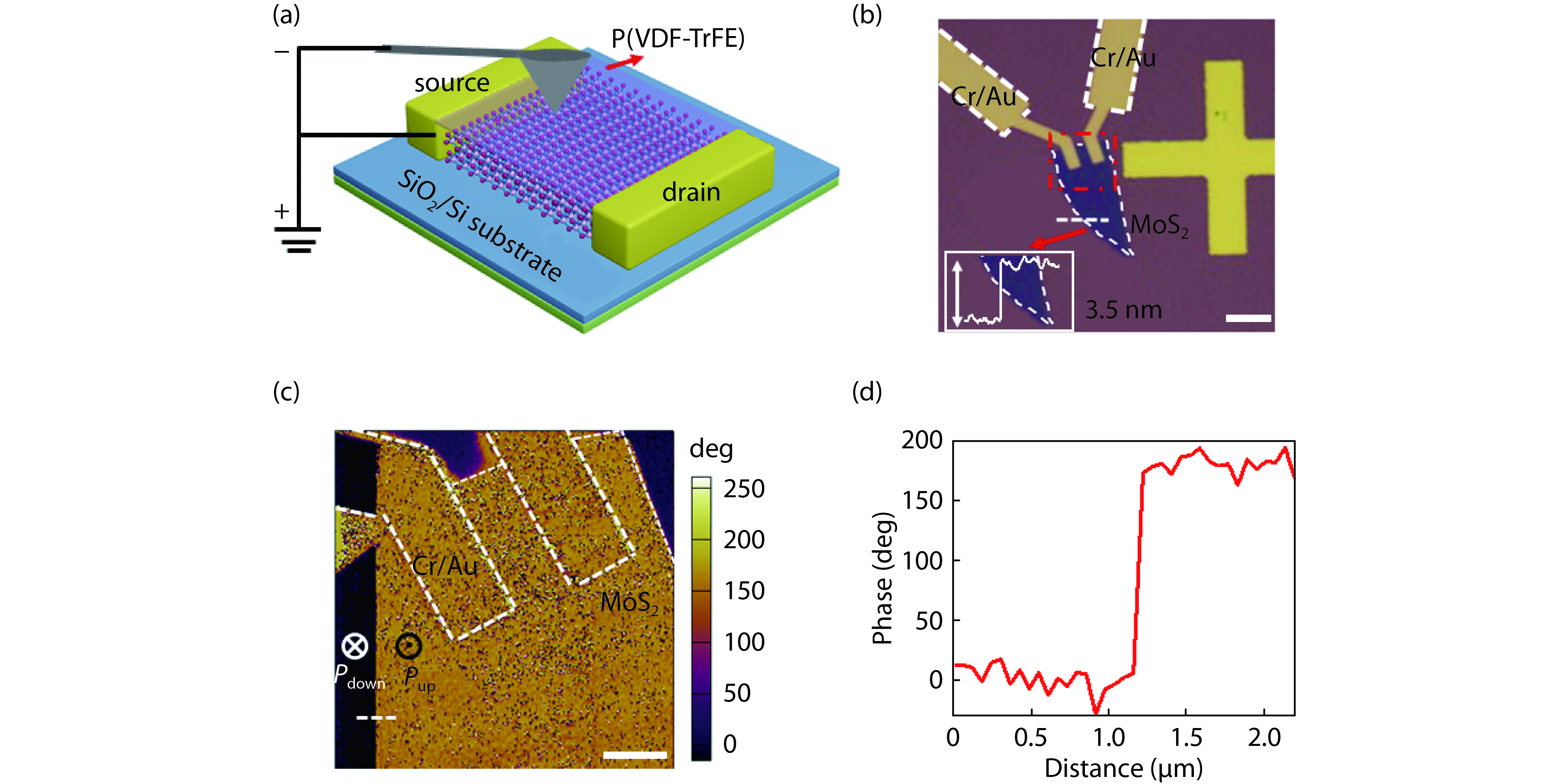
    Fig. 2. (Color online) Structure illustration of the gate-free MoS2 photodetector. (a) A 3D schematic of the device structure. (b) The optical image of the device, which includes a 3.5 nm MoS2 and Cr/Au source and drain electrodes covered by 50 nm-thick P(VDF-TrFE) film, scale bar is 10 μm. (c) The PFM phase image of the device (red square part in (b)), two polarization states of Pdown and Pup represent the opposite direction of the electric dipole moment in different parts (orange and black), scale bar is 3 μm. (d) Phase profile extracted along the white dashed line in (c), which demonstrated that the MoS2 in the channel has a 180° phase difference with the other part.
    (Color online) Electrical characteristics of the device with three different polarization states of P(VDF-TrFE). (a) The Isd–Vsd characteristics of the device with three different polarization states of P(VDF-TrFE). These three polarization states are fresh (without polarization), Pup (upward polarization) and Pdown state (downward polarization). (b) Sectional view of the device for illustrating the distribution of electron and hole under downward and (c) upward polarization state. (d–f) The energy band diagrams of the device with three polarization states at Vsd = 0 V. Φb is the Schottky barrier height, Eg is the energy gap of MoS2, δ is the barrier height from conduction band to Fermi level.
    Fig. 3. (Color online) Electrical characteristics of the device with three different polarization states of P(VDF-TrFE). (a) The IsdVsd characteristics of the device with three different polarization states of P(VDF-TrFE). These three polarization states are fresh (without polarization), Pup (upward polarization) and Pdown state (downward polarization). (b) Sectional view of the device for illustrating the distribution of electron and hole under downward and (c) upward polarization state. (d–f) The energy band diagrams of the device with three polarization states at Vsd = 0 V. Φb is the Schottky barrier height, Eg is the energy gap of MoS2, δ is the barrier height from conduction band to Fermi level.
    (Color online) Optoelectronic properties of the device. (a) Isd–Vsd curves of the device under dark and different power of incident light (520 nm). (b) photocurrent switching characteristic of the device with 520 nm laser illumination. The light power is 6.56 μW and Vsd = 1 V. (c) The photocurrent map of the device recorded at Pup state and Vsd = 1 V, the incident light power is 0.28 μW, scale bar = 3 μm. (d, e) The photocurrent rise and fall time extracted from a photocurrent switching cycle. (f) The photoresponse characteristic of the device under incident light with the different wavelengths but the same power.
    Fig. 4. (Color online) Optoelectronic properties of the device. (a) IsdVsd curves of the device under dark and different power of incident light (520 nm). (b) photocurrent switching characteristic of the device with 520 nm laser illumination. The light power is 6.56 μW and Vsd = 1 V. (c) The photocurrent map of the device recorded at Pup state and Vsd = 1 V, the incident light power is 0.28 μW, scale bar = 3 μm. (d, e) The photocurrent rise and fall time extracted from a photocurrent switching cycle. (f) The photoresponse characteristic of the device under incident light with the different wavelengths but the same power.
    DescriptionResponse time (s)Wavelength (nm)Gate voltage /BiasRef.
    MoS2–SiO2–Si back gate 2532Vg= 100 V, Vsd= 5 V [27]
    MoS2–SiO2–Si back gate (CVD) 3532Vg= 40 V, Vsd= 1 V [17]
    MoS2–Al2O3–ITO top gate 0.3580Vg= –9 V, Vsd= 1 V [28]
    MoS2–SiO2–Si back gate 0.05488Vg= 50 V, Vsd= 1 V [29]
    MoS2–P(VDF-TrFE) 1.2 × 10–4520Vg= 0 V, Vsd= 1 V This work
    Table 1. Photoresponse speed comparation between our device and other MoS2-based photodetectors.
    Shuaiqin Wu, Guangjian Wu, Xudong Wang, Yan Chen, Tie Lin, Hong Shen, Weida Hu, Xiangjian Meng, Jianlu Wang, Junhao Chu. A gate-free MoS2 phototransistor assisted by ferroelectrics[J]. Journal of Semiconductors, 2019, 40(9): 092002
    Download Citation