
Shuaiqin Wu, Guangjian Wu, Xudong Wang, Yan Chen, Tie Lin, Hong Shen, Weida Hu, Xiangjian Meng, Jianlu Wang, Junhao Chu. A gate-free MoS2 phototransistor assisted by ferroelectrics[J]. Journal of Semiconductors, 2019, 40(9): 092002
- Journal of Semiconductors
- Vol. 40, Issue 9, 092002 (2019)
Abstract
1. Introduction
Two-dimensional (2D) materials have attracted extensive attention all over the world in past decades. More and more new 2D materials have been found and novel device structures emerge in endlessly[
Furthermore, most of these phototransistors rely on a real metal gate to apply a gate voltage then to reduce the dark current, leading to leakage between source/drain and gate, but usually, it is difficult to reduce the dark current in a satisfying level[
Here, we report the fabrication and operation of a gate-free MoS2 phototransistor utilizing the remnant polarization field of P(VDF-TrFE) to modulate the carrier concentration in MoS2. Instead of a metal gate, piezoelectric force microscopy (PFM) is employed to polarize P(VDF-TrFE) under resonant mode in this work. The ferroelectric field has two polarized directions with a local electric field of 109 V/m which is large enough to tune MoS2 to completely depleted and accumulated state[
2. Experimental methods
PFM measurements were carried out at room temperature on a commercial atomic force microscope (Bruker Multimode 8, Camarillo, CA, USA). Positive and negative DC voltage were applied on P(VDF-TrFE) by a commercial silicon tip (Budget Sensors) covered with chromium/platinum under a contact resonance frequency of 0.7 MHz typically. When applied voltage by PFM probe, the sample will deform and cause the deflection of cantilever. Such a change can be measured to reflect the piezoelectric properties of the sample. For poly(vinylidene fluoride-trifluoroethylene) (P(VDF-TrFE)) copolymers used in this work, when a positive voltage applied on it, the domains will point down vertically while for negative voltage, the domains will point up vertically.
3. Results and discussion
3.1. Ferroelectric switching
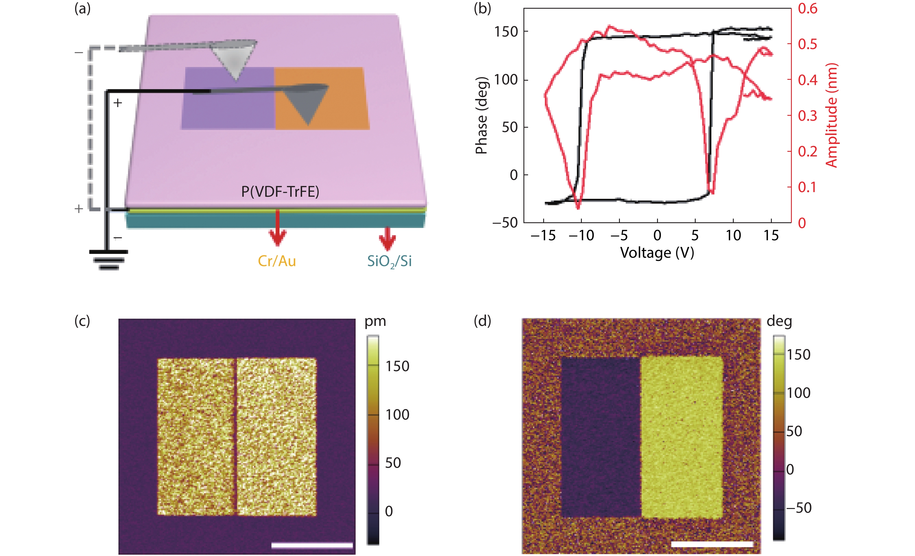
Fig. 1(a) shows the schematic diagram of the operation for P(VDF-TrFE) polarization switching with PFM. The P(VDF-TrFE) film (50 nm) was spin-coated on the top of chromium/gold (Cr/Au) bottom electrode. The thickness of Cr and Au is 3 and 7 nm, respectively, which is prepared on a 285-nm-thick SiO2 substrate by thermal evaporation. A DC bias is applied to the P(VDF-TrFE) through the PFM tip, and the bottom electrode is grounded. Fig. 1(b) shows the out-of-plane PFM signals of this P(VDF-TrFE) film. The amplitude signal represents the absolute magnitude of the local piezoelectric response, while the phase signal reveals the polarization direction in every individual domain[
![]()
Figure 1.(Color online) Ferroelectric polarization switching by PFM for 50 nm-thick P(VDF-TrFE) film. (a) Schematic of the operation for P(VDF-TrFE) polarization switching with PFM probe appling a positive or negative voltage. (b) The PFM amplitude (red) and phase (black) hysteresis loops during the switching process, scale bar is 10 μm. (c) Amplitude signal and (d) phase signal of the P(VDF-TrFE) film after writing half-to-half rectangle patterns with reversed DC bias, scale bar is 10 μm.
Fig. 2(a) illustrates the configuration of the gate-free MoS2 phototransistor. The MoS2 was obtained by the Scotch tape-based mechanical exfoliation method, then transferred on the highly doped silicon substrate covered with a 285-nm-thick SiO2. The source/drain electrode is Cr/Au which was prepared by electron beam lithography, thermal evaporation, and lift-off steps. The thickness of Cr and Au is 10 and 20 nm, respectively. Subsequently, the device was annealed at 200 °C for 2 h in an argon atmosphere. At last, 50 nm P(VDF-TrFE) film was spin-coated on the device and annealed at 135 °C for 2 h in an oven to enhance its crystallinity. The optical image of the device can be seen in Fig. 2(b) and the thickness of MoS2 in this work is 3.5 nm measured by AFM (See the insert in Fig. 2(b)). The MoS2 channel length is set to 5 μm. PFM was used to polarize P(VDF-TrFE) in different directions. As shown in Fig. 2(c), different regions of P(VDF-TrFE) on MoS2 were polarized upward or downward. Fig. 2(d) shows the polarization phase signal extracted near the domain wall (Fig. 2(c)), a clear reversal of 180° can be found which reveals the MoS2 is modulated by a downward polarization field.
![]()
Figure 2.(Color online) Structure illustration of the gate-free MoS2 photodetector. (a) A 3D schematic of the device structure. (b) The optical image of the device, which includes a 3.5 nm MoS2 and Cr/Au source and drain electrodes covered by 50 nm-thick P(VDF-TrFE) film, scale bar is 10 μm. (c) The PFM phase image of the device (red square part in (b)), two polarization states of
3.2. Electrical properties and photoresponse properties
The electrical properties of the device were firstly studied. Fig. 3(a) shows the Isd–Vsd characteristics under three different polarization states of P(VDF-TrFE). When a DC positive voltage is applied to the P(VDF-TrFE), the polarization direction is downward and the MoS2 channel is in a carrier accumulation state (Pdown state). Conversely, the polarization direction is upward and the MoS2 channel is in a carrier depletion state (Pup state) when a DC negative voltage is applied. It can be obviously found that the channel current of the device in Pdown state is larger than that in the fresh state by an order of magnitude, while the current in Pup state decreased into below 10–11 A, smaller than that in fresh state by more than 4 orders of magnitude. As a result, such an ultra-low dark current of the device in Pup state is very beneficial for photodetector operation. The sectional view of the device and the transport of carriers under two different polarization states (the Pup state and Pdown state) are shown in Figs. 3(b) and 3(c). Fig. S3 presents the transfer characteristics of the device, it can reveal that MoS2 used in this work is an intrinsic n-type semiconductor. As a result of electrostatic induction, when P(VDF-TrFE) is in Pdown state, the electrostatic field from the remnant polarization makes the n-type MoS2 channel in an accumulated state (Fig. 3(b)); when P(VDF-TrFE) is in Pup state, the electrostatic field changes into the opposite direction and the channel is in a depleted state (Fig. 3(c)). Fig. 3(d)–3(f) reveals the equilibrium band structure of MoS2 when P(VDF-TrFE) is in three different polarization states. Fermi level (EF) is defined as an energy level that the probability for an electron to take up is equal to 1/2. The Fermi level is close to conduction band for n-type semiconductors but close to valence band for p-type semiconductors. As shown in Fig. 3(d), the Fermi level of MoS2 is close to the conduction band when P(VDF-TrFE) is in the fresh state. After applying a positive voltage to P(VDF-TrFE) by the PFM, a downward polarization field will be applied to the MoS2. Then, the position of Femi level moves up and more electrons can take part in conduction, as shown in Fig. 3(e). In this case, if put the device under illumination and apply a drain bias to read the channel current, the photon-generated current will be covered up by the thermionic or tunneling current[
![]()
Figure 3.(Color online) Electrical characteristics of the device with three different polarization states of P(VDF-TrFE). (a) The
Next, the optoelectronic performance of the device is comprehensively studied. A 520 nm laser is employed as the light source in these measurements. It is widely known that the photocurrent generation mechanism for MoS2 photodetector is a photoconductive effect[
![]()
Figure 4.(Color online) Optoelectronic properties of the device. (a)
The photoresponse time is another important parameter to evaluate the ability of photodetectors, which is defined as the time for the photocurrent switching from 10% to 90%. For our device, the photocurrent turns from off to on state is as fast as 200 μs (Fig. 4(d)), indicating a fleet generation of photo-generated electron–hole pairs in MoS2. It takes 120 μs for the device to turns from on to off state (Fig. 4(e)), indicating a fast process of carrier recombination. The photoresponse speed of our device is faster than those intrinsic MoS2 photodetectors (see Table 1)[
4. Summary
In summary, we have fabricated a gate-free MoS2 phototransistor assisted by ferroelectric domain. Under the modulation of remnant polarization field, the carrier concentration of the MoS2 channel is completely depleted and the optoelectronic performance of the device is greatly enhanced. The dark current of the MoS2 photodetector is reduced to the order of several picoamperes. The photoresponse time is also improved to 200 and 120 μs, which is much faster than those intrinsic MoS2 photodetectors without P(VDF-TrFE). More importantly, such a gate-free MoS2 phototransistor assisted by the ferroelectric domain embraces the ultra-low power consumption. Therefore, it provides a reliable way to develop 2D materials-based photodetectors with high-performance and ultra-low power consumption.
Acknowledgments
This work was partially supported by the Major State Basic Research Development Program (Grant Nos. 2016YFA0203900, 2016YFB0400801 and 2015CB921600), and Key Research Project of Frontier Sciences of Chinese Academy of Sciences (Nos. QYZDB-SSW-JSC016, QYZDY-SSW-JSC042). Strategic Priority Research Program of Chinese Academy of Sciences (XDPB12, XDB 3000000). Natural Science Foundation of China (Grant Nos. 61521001, 61574151, 61574152, 61674158, 61722408, 61734003 and 61835012), and Natural Science Foundation of Shanghai (Grant No. 16ZR1447600, 17JC1400302).
References
[1] J Wang. A novel spin-FET based on 2D antiferromagnet. J Semicond, 40, 020401(2019).
[2] W Jiang, X Wang, Y Chen et al. Large-area high quality PtSe2 thin film with versatile polarity. InfoMat, 1, 260(2019).
[3] G Wu, X Wang, Y Chen et al. Ultrahigh photoresponsivity MoS2 photodetector with tunable photocurrent generation mechanism. Nanotechnology, 29, 485204(2018).
[4] L Liu, X Wang, L Han et al. Electrical characterization of MoS2 field-effect transistors with different dielectric polymer gate. AIP Adv, 7, 065121(2017).
[5] S Xue, X L Zhao, J L Wang et al. Preparation of La0.67Ca0.23- Sr0.1MnO3 thin films with interesting electrical and magnetic properties via pulsed-laser deposition. Sci Chin Phys, Mechan, Astron, 60, 027521(2017).
[6] J Wang, H Fang, X Wang et al. Recent progress on localized field enhanced two-dimensional material photodetectors from ultraviolet-visible to infrared. Small, 13, 1700894(2017).
[7] Y W Son, M L Cohen, S G Louie. Energy gaps in graphene nanoribbons. Phys Rev Lett, 97, 216803(2006).
[8] J C Meyer, A K Geim, M I Katsnelson et al. The structure of suspended graphene sheets. Nature, 446, 60(2007).
[9] H Peelaers, C G Van de Walle. Effects of strain on band structure and effective masses in MoS2. Phys Rev B, 86, 241401(2012).
[10] D H Kang, M S Kim, J Shim et al. High-performance transition metal dichalcogenide photodetectors enhanced by self-assembled monolayer doping. Adv Funct Mater, 25, 4219(2015).
[11] L Wang, J Jie, Z Shao et al. MoS2/Si heterojunction with vertically standing layered structure for ultrafast, high-detectivity, self-driven visible-near infrared photodetectors. Adv Funct Maters, 25, 2910(2015).
[12] D Jariwala, V K Sangwan, C C Wu et al. Gate-tunable carbon nanotube-MoS2 heterojunction pn diode. Proc Nat Acad Sci, 110, 18076(2013).
[13] K S Novoselov, A K Geim, S V Morozov et al. Electric field effect in atomically thin carbon films. Science, 306, 666(2004).
[14] R Addou, L Colombo, R M Wallace. Surface defects on natural MoS2. ACS Appl Mater Interfaces, 7, 11921(2015).
[15] A Di Bartolomeo, L Genovese, F Giubileo et al. Hysteresis in the transfer characteristics of MoS2 transistors. 2D Mater, 5, 015014(2017).
[16] J Kwon, Y K Hong, G Han et al. Giant photoamplification in indirect-bandgap multilayer MoS2 phototransistors with local bottom-gate structures. Adv Mater, 27, 2224(2015).
[17] W Zhang, J K Huang, C H Chen et al. High-gain phototransistors based on a CVD MoS2 monolayer. Adv Mater, 25, 3456(2013).
[18] C L Wu, J W. Chen C H Chen et al. A gate-free monolayer WSe2 pn diode. APS Meeting Abstracts(2018).
[19] C Baeumer, D Saldana-Greco, J M P Martirez et al. Ferroelectrically driven spatial carrier density modulation in graphene. Nat Commun, 6, 6136(2015).
[20] C Yin, X Wang, Y Chen et al. A ferroelectric relaxor polymer-enhanced p-type WSe2 transistor. Nanoscale, 10, 1727(2018).
[21] B B Tian, J L Wang, S Fusil et al. Tunnel electroresistance through organic ferroelectrics. Nat Commun, 7, 11502(2016).
[22] X Wang, P Wang, J Wang et al. Ultrasensitive and broadband MoS2 photodetector driven by ferroelectrics. Adv Mater, 27, 6575(2015).
[23] D Kufer, G Konstantatos. Highly sensitive, encapsulated MoS2 photodetector with gate controllable gain and speed. Nano Lett, 15, 7307(2015).
[24] H S Lee, S W Min, M K Park et al. MoS2 nanosheets for top-gate nonvolatile memory transistor channel. Small, 8, 3111(2012).
[25] E Zhang, W Wang, C Zhang et al. Tunable charge-trap memory based on few-layer MoS2. ACS Nano, 9, 612(2014).
[26] D Zhao, I Katsouras, K Asadi et al. Switching dynamics in ferroelectric P (VDF-TrFE) thin films. Phys Rev B, 92, 214115(2015).
[27] M M Furchi, D K Polyushkin, A Pospischil et al. Mechanisms of photoconductivity in atomically thin MoS2. Nano Lett, 14, 6165(2014).
[28] H S Lee, S W Min, Y G Chang et al. MoS2 nanosheet phototransistors with thickness-modulated optical energy gap. Nano Lett, 12, 3695(2012).
[29] H Li, J Wu, Z Yin et al. Preparation and applications of mechanically exfoliated single-layer and multilayer MoS2 and WSe2 nanosheets. Acc Chem Res, 47, 1067(2014).
[30] A Gruverman, S V Kalinin. Piezoresponse force microscopy and recent advances in nanoscale studies of ferroelectrics. J Mater Sci, 41, 107(2006).
[31] X Chen, Z Wu, S Xu et al. Probing the electron states and metal-insulator transition mechanisms in molybdenum disulphide vertical heterostructures. Nat Commun, 6, 6088(2015).
[32] E J G Santos, E Kaxiras. Electrically driven tuning of the dielectric constant in MoS2 layers. ACS Nano, 7, 10741(2013).
[33] Y Xie, B Zhang, S Wang et al. Ultrabroadband MoS2 photodetector with spectral response from 445 to 2717 nm. Adv Mater, 29, 1605972(2017).
[34] O Lopez-Sanchez, D Lembke, M Kayci et al. Ultrasensitive photodetectors based on monolayer MoS2. Nat Nanotechnol, 8, 497(2013).
[35] K M McCreary, A T Hanbicki, J T Robinson et al. Large-area synthesis of continuous and uniform MoS2 monolayer films on graphene. Adv Funct Mater, 24, 6449(2014).
[36] M Long, P Wang, H Fang et al. Progress, challenges, and opportunities for 2D material based photodetectors. Adv Funct Mater, 29, 1803807(2019).
[37] L Yin, Z Wang, F Wang et al. Ferroelectric-induced carrier modulation for ambipolar transition metal dichalcogenide transistors. Appl Phys Lett, 110(2017).
[38] W Choi, M Y Cho, A Konar et al. High-detectivity multilayer MoS2 phototransistors with spectral response from ultraviolet to infrared. Adv Mater, 24, 5832(2012).


Set citation alerts for the article
Please enter your email address

© Copyright 2018-2021 | Chinese Laser Press. All Rights Reserved 沪ICP备15018463号-20