Trevon Badloe, Seokho Lee, Junsuk Rho, "Computation at the speed of light: metamaterials for all-optical calculations and neural networks," Adv. Photon. 4, 064002 (2022)
Copy Citation Text
The explosion in the amount of information that is being processed is prompting the need for new computing systems beyond existing electronic computers. Photonic computing is emerging as an attractive alternative due to performing calculations at the speed of light, the change for massive parallelism, and also extremely low energy consumption. We review the physical implementation of basic optical calculations, such as differentiation and integration, using metamaterials, and introduce the realization of all-optical artificial neural networks. We start with concise introductions of the mathematical principles behind such optical computation methods and present the advantages, current problems that need to be overcome, and the potential future directions in the field. We expect that our review will be useful for both novice and experienced researchers in the field of all-optical computing platforms using metamaterials.
Computers and digital processors that are used daily by a large number of people in modern society are now an integral part of life. They are generally made up of numerous transistors, resistors, capacitors, and sensors that communicate through the flow of electrons to perform calculations and store information using bits that are represented by either a “0” or “1.” As the amount of online digital content being created and consumed increases continuously, the demands for data transfer, storage, and larger bandwidths are simultaneously rising. However, the physical size of transistors is reaching the angstrom scale, meaning that further reduction in size will be limited by the size of atoms themselves. Various new technologies have been proposed as new ways to perform calculations with higher speed and efficiency. Notably, quantum computing and photonic computing are two of the major advancements that are being actively researched.1 Both have their individual merits and obstacles that must be overcome for application in real-life situations. Quantum computing promises increased parallelism and therefore raw speed, but at the moment, must run at extremely low temperatures that require a lot of power and specialized equipment.2 Photonic computing, on the other hand, aims to replace electronic systems with their photonic equivalent to simultaneously increase the speed and efficiency of data processing3 and decrease the amount of data corruption that can occur in electronics due to the lack of interference of photons compared to electrons but is somewhat hindered by the requirements of wavelength scale building blocks, which are tens to hundreds of times larger than the latest electronics architectures that use a 3-nm die.4 As both of these technologies are in their infancy, there is still a long way for them to mature before being commercially viable, by which time, they could potentially be complementary, rather than competing, technologies.
Research into photonic devices for all-optical computations has been fruitful over the past few decades.5–12 All-optical analog computing opens the door for large real-time parallel computations with minimal energy requirements, which in the energy-conscious reality that we live in with such massive reliance on big data calculations, practical realizations of low-energy real-time image, and data processing could be fundamental to unlocking the next generation of all-optical, or optoelectronic devices. Rather than using the standard “0” and “1” bits used for digital calculations and postprocessing of data, electromagnetic (EM) fields can be exploited to perform calculations and operations optically at the speed of light. Such analog processing can exploit all of the optical properties of light simultaneously, including the phase, amplitude, and polarization to manipulate the complex amplitude of EM waves. This could facilitate both high-throughput and low-power devices, all inside a miniaturized footprint, compared to that of traditional bulky optics made up of lenses and other components. Silva et al.13 proposed the concept of using metamaterials for spatial differentiation, integration, or convolution, with simulations based on metasurfaces combined with graded-index waveguides, as well as multilayered slabs designed to achieve specific Green’s functions. Since then, there have been numerous experimental demonstrations of optical calculations using metamaterials in various wavelength regimes. Along with the development of high-fidelity and large-scale nanofabrication techniques that have been produced over the past decade, the opportunity to create fully on-chip photonic devices with extremely miniaturized footprints appears to have come to light. Fully optical computing and image processing could have impacts on numerous fields, including on-chip solid-state light detection and ranging (LiDAR),14,15 bioimaging,16 and preprocessing of big data.17
Here we will review the recent advancements of all-optical photonic calculations using metamaterials, including simple single-layered structures, multilayer structures, structured flat optical elements, known as metasurfaces, and other photonic devices, such as photonic crystals. We note here that although photonic crystals are not exactly classified as metamaterials, they are still photonic devices that demonstrate interesting characteristics at the wavelength scale, which become nanophotonic devices for visible light. We will start by introducing the basic mathematical functions that underpin the speed-of-light calculations. We will then introduce the latest research on metamaterials for linear differentiation, integration, and Laplacian calculations and discuss their potential applications in terms of all-optical computing. We will conclude by discussing the current progress in all-optical machine learning, from the mathematical basis of how it works, to the latest research, and current difficulties. We will finally provide our thoughts on the outlook and future of all-optical computing toward fully integrated photonic brains. We hope that this review will be useful for both experts and novices in the field of all-optical computations using metamaterials and to serve as a valuable reference to guide new research.
Sign up for Advanced Photonics TOC. Get the latest issue of Advanced Photonics delivered right to you!Sign up now
2 All-Optical Calculations at the Speed of Light
2.1 Mathematical Operations
We start by describing how light can be used to perform mathematical operations. An interesting mathematical parallel exists between convolution in Fourier space between the input function and the systems impulse response, and the interaction of a single-wavelength EM wave interacting with an optical element. That is, for a system with an impulse response given by , any input function given by produces an output of that can be defined by which can be written in terms of Fourier transforms (FTs) as where IFT denotes an inverse Fourier transform, and , where and are the spatial frequency variables and and are real-space locations. This is analogous to an input EM wave given by that interacts with a metamaterial imparting a spatially varying function that performs some form of optical operation in Fourier space. The resultant EM field, can be defined as
It is therefore clear to see that the phase and amplitude that are encoded by the metamaterial represent the term in Eq. (2). It should be noted that, although it does not cause any additional difficulties, based on the well-known identity , the output EM field will be flipped, i.e., it will represent . This FT is generally performed using standard refractive lenses but has also been successfully encoded directly into a metamaterial itself to further miniaturize the system. This switching between real and Fourier space can also be avoided by designing metamaterials that directly process the required transfer function in the Fourier space. This is generally achieved by designing a metamaterial with an angular-dependent response and has been termed as the Green’s function approach.
Differentiation is one of the fundamental mathematical operations that appears in numerous places in physics, from Newton’s famous second law of motion, to Maxwell’s equations that underpin classical electromagnetism. When applied to an image, a process of edge detection is performed, which could have potential impact in numerous fields that benefit from instantaneous edge detection without the need for computationally expensive and time-costly postprocessing, such as in object and scene detection or biomicroscopy. Machine-learning algorithms also rely on such numerical calculations, such as differentiation and backpropagation, further highlighting the potential for all-optical computing at the speed of light. First, without loss of generality, we consider one-dimensional (1D) operations and use the notation of to represent the optical coefficient of the metamaterial, which could be interchanged freely with the reflection or transmission coefficient, and , respectively, depending on the metamaterial design and direction of operation.
2.1.1 First-order differentiation
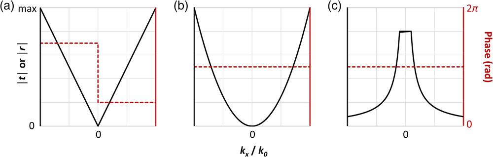
In order to perform first-order spatial differentiation in 1D, for an arbitrary function , the operation is equal to in Fourier space. Therefore, the metamaterial should physically impart the transfer function: where is the size of the metamaterial bounding the spatial locations . This function is depicted in Fig. 1(a). The maximum reflection or transmission that can be achieved imparts a limitation that is related to the fact that the operations performed by the metamaterials are in fact scaled when compared to the exact mathematical definition. The phase of the transfer function required for first-order differentiation is odd with respect to , which necessarily requires some form of mirror symmetry to be broken with respect to the axis as well as the axis.18 This also holds true for other odd integer orders of differentiation. In terms of optical image processing, the first-order differential will produce an edge-enhanced image. Since the first derivative is dependent only on the neighboring intensities, it can be quite sensitive to fluctuations and noise in the image.
Figure 1.Required optical transfer functions for all-optical calculations for (a) first- and (b) second-order differentiation and (c) integration. The black lines represent the required transmission or reflection coefficients, whereas the red dashed lines denote the required phase. Note the phase shift required at for the first-order differentiation, due to its being an odd function. The absolute value of the phase is arbitrary. The limits of the axis are determined by the angular response of the designed metamaterial, which denotes the working NA of the system. Note the arbitrary truncated region around 0 for the integration operation that is necessary to avoid unphysical gain requirements, as suggested in Ref. 13.
Considering an arbitrary function , second-order spatial differentiation in 1D, i.e., , can be represented in Fourier space as . This means that designing a metamaterial that imparts a parabolic transfer function and a near-constant phase profile to the incoming EM wave allows access to completely optical second-order differentiation, i.e., the following function should be achieved: where the coefficient is the same as Eq. (4). This function is depicted visually in Fig. 1(b). Since , the transmission or reflection should be zero at normal incidence, while increasing quadratically under increasing angle of incidence. Second-order differentiation is generally less prone to noise in images but can, however, struggle when there are large local fluctuations in intensity.
2.1.3 Integration
To perform 1D integration on an arbitrary function , the operation defined by must be achieved. It should be noted that the singularity at should be taken care of appropriately when designing the metamaterial.13 This has been achieved through the use of a constant value around the singularity. This function is depicted in Fig. 1(c). In all-optical image processing, the integral of an image has implications in real-time face detection, where high-resolution images can be processed quickly to uncover and highlight important features.19
Although we introduced 1D operation for simplicity, two-dimensional (2D) operations can be easily achieved by simply including the second dimension. The Laplacian is a specific example of a well-known 2D operation that can be implemented by manipulating EM waves.
2.1.4 Laplacian
The Laplacian () is the 2D version of the second-order differentiation operation discussed above. Therefore, for a function , the 2D second-order differentiation is given as . Subsequently, given an arbitrary EM field , , where . This results in an additional requirement that the metamaterial should be symmetrical in both the and directions. Such even operations are fairly simple to achieve physically; however, for odd functions extra steps must be undertaken to create a physical asymmetry. Various solutions have been proposed and developed, which we will review in terms of all-optical mathematical operations with different designs of metamaterials and photonic devices in the following section.
2.2 Metamaterials for All-Optical Calculations
2.2.1 Static metamaterials
Single and multilayers
The simplest way of manipulating EM waves is by passing them through the interface between two media. Since layering materials does not require any form of patterning or complex procedures other than deposition, they provide an obvious and straightforward method of manipulating EM waves through the correct design of the wavelength, incident angle, and thicknesses. Fabry–Perot (FP) resonators have found wide use in metamaterials for various applications from selective absorbers20,21 and radiative cooling,22 to structural color, with multilayer structures such as distributed Bragg reflectors being extensively researched. They have also been utilized for all-optical computing through various mechanisms, which will be presented here.
In one of the first examples of optical computing using metamaterials, Zhu et al.23 utilized surface plasmon polaritons (SPPs) to demonstrate first-order differentiation using a simple single layer of silver on a glass prism [Figs. 2(a)–2(c)]. The total reflected amplitude was determined by the interference between the reflection from the glass–metal interface and the SPP radiation under the illumination of 532 nm incident light. The thickness of the film was only around 50 nm, providing a tiny footprint for the device that has the potential to be produced at scale. The minimum resolution of edge detection was determined to be around , which could be sufficient for image-processing applications. However, the device operates in quite a narrow spatial region with limited efficiency due to the requirement of exciting the SPP, which in turn, also restricts the design to work in reflection. The requirement of the use of a bulky prism, also somewhat offsets the benefit of the reduction of size of the super-thin film. By adding a few extra layers, rather than the extremely simple single layer reported previously, Wesemann et al.24 experimentally showed the use of a near-perfect absorbing mirror for all-optical image processing of phase and amplitude objects with a Salisbury screen with a two-layer design [Figs. 2(d)–2(f)]. The metal–insulator–metal layers made up of gold (Au) and silicon dioxide () provide an FP response, so by making the dielectric insulator layer thickness approximately a quarter wavelength, perfect absorption is released at the working wavelength. Since this absorption is dependent on the incident angle of light (), the reflectance is therefore also related, since the transverse component , where is the wave vector of light in free space. The successful demonstration of phase imaging of a biological sample using the designed device highlights the potential for such simple systems, without any requirements for complex and time-consuming structuring processes, to achieve all-optical computation.
Figure 2.All-optical calculations using planar films. (a) Experimentally measured (green dots) and numerically fitted (solid lines) spatial transfer functions for three different samples. corresponds to the incident angle required for the phase matching to support the SPP. All optical first-order differentiation of (b) (i) amplitude and (c) (i) phase images. (ii) The reflected intensity after differentiation. Scale bars, . (d) Calculated reflectance for p-polarization (solid line) and s-polarization (dashed line) at the absorption wavelength of 631 nm. (e) Demonstration of edge enhancement in reflected amplitude images. (i) Bright-field microscope image of the amplitude object and experimentally reflected image from the thin film mirror at (ii) 598 nm, (iii) 640 nm, and (iv) 694 nm. Scale bar, . (f) Experimental demonstration of phase imaging of a biological sample. Images reflected from the mirror at (i) 598 nm (ii), 638 nm, and (iii) 694 nm. Scale bar, . First-order differentiation using the SHE of light. (g) Experimental (dots), theoretical (dashed lines), and the ideal (solid lines) spatial spectral transfer functions for first-order differentiation. (h) Experimental demonstration of the material and angle independence of SPE of light for image differentiation; (i) air to glass interface with the Chinese character for “light” and (ii) air to Au and glass interface with the English word “LIGHT.” Images (a)–(c) reproduced with permission from Ref. 23. Copyright 2017 Springer Nature Group. Images (d)–(f) reproduced with permission from Ref. 24. Copyright 2019 AIP Publishing LLC. Images (h)–(j) reproduced with permission from Ref. 25. Copyright 2019 American Physical Society.
Noting the fact that most multilayered structures can only operate for even functions, such as second-order differentiation, due to their inherent symmetry, Youssefi et al.26 provided a solution to achieve odd functions, specifically first-order differentiation. This was achieved by simply rotating the device, or equivalently, using light at an oblique incidence. Since the reflection coefficient of TM-polarized light becomes zero at the Brewster angle, odd functions can be subsequently released; however, they are limited to 1D operation. However, Xu et al.27 later provided a solution for 2D differentiation using the properties of the Brewster angle. 2D edge detection was also demonstrated by Zhu et al.28. They identified that the complex transfer function should carry a topological charge (TC) in order to exhibit broadband isotropic 2D differentiation. By selecting the appropriate input and output polarization and using the incident angles that correspond to total internal reflection or the Brewster angle, 2D differentiation was successfully proven for both green and red light with wavelengths of 532 and 633 nm.
In addition to exploiting the Brewster angle, Zhu et al.25 showed that since the reflected light from a planar interface exhibits a different transverse shift based on its polarization state, the spin Hall effect (SHE) of light can be utilized for spatial differentiation of EM waves [Figs. 2(g)–2(j)]. They showed that by using specific orthogonal polarization states under the paraxial approximation, the reflected and refracted light from any planar interface, regardless of the material or incident angle, can be employed, since the differentiation operation is due to the intrinsic nature of the SHE.29 Since SHE is a nonresonant effect, the spatial differentiation frequency bandwidth is infinitely large, which enables ultrafast all-optical calculations at all wavelengths. Accordingly, 1D differentiation was experimentally demonstrated at a wavelength of 532 nm, both for various angles and an air–glass and an air–Au–glass interface, proving the generality of using SHE for differentiation. One drawback of SHE is that it disappears at normal incidence, which means that the signal is decreased at extremely small incident angles. However, recently, SHE has been proven for arbitrarily polarized and unpolarized light,30 as well as high-efficiency operation,31 which could open the path for further developments of SHE for all-optical calculations. Another interesting application of spatial differentiation using SHE was demonstrated as a method to calibrate spatial light modulators (SLMs) by converting phase information into amplitude information that can be imaged directly.32 In turn, this concept was extended to develop a phase-mining method by measuring a shadow-cast effect in the measured images.33 2D differentiation has also been proposed using SHE near the Brewster angle due to a double-peak profile.34 A common drawback of the work presented so far is that they operate in reflection mode, whereas for practical applications, transmission mode would be preferred.
This was successfully proposed and demonstrated by Xue and Miller,35 who also noted that the conventional Laplacian-based transmission response may be not the ideal case when considering the scattering physics of real-world designs. Therefore, through the optimization of alternating layers of silicon (Si) and , 2D second-order differentiation was demonstrated with a high numerical aperture (NA), along with the benefits of straightforward fabrication of simple multilayers. Transmission up to angles of 80 deg was designed, which corresponds to an NA of 0.98. Since any transmission function can be optimized by changing the target, various operations were designed. In particular, for the functionality of edge detection, the authors suggest that since a multilayer design with a transmission dependency is more closely designed than the standard quadratic form, suggesting that a more data-driven approach could be taken to optimize the output fields rather than designing the optical response of the metamaterial directly. Other multilayer dielectric slabs have also been proven for integration calculations.36
Plasmonic structures
Pors et al.37 demonstrated plasmonic metasurfaces for analog computing by exciting gap-surface plasmons (GSPs) through the design of an Au meta-atom on top of a spacer, above an Au mirror [Figs. 3(a)–3(c)]. The GSPs propagate within the spacer, demonstrating FP-like resonances that originate from the multiple reflections due to the meta-atoms. Both first-order differentiation and integration were demonstrated numerically and experimentally. The metasurfaces operate in reflection mode at the wavelength of 800 nm, providing all-optical mathematical operations at visible wavelengths. The fundamental design of using the GSP allows for the full phase and amplitude control of incident light; however, it must be used in reflection, which somewhat limits its potential uses for integration in optical systems that generally require transmission-type components. Hwang et al.38 subsequently numerically presented a transmission mode plasmonic metasurface based on localized surface plasmon resonances driven by evanescent coupling of five metallic meta-atoms [Fig. 3(d)]. Simulations of second-order differentiation of phase were demonstrated; however, gaps of around 10 nm could limit the feasibility of fabrication of such devices. Various double split ring resonator (SRR) devices have been developed to perform second-order differentiation in the microwave regime.40 Recently, a double SRR fabricated on either side of a dielectric substrate was demonstrated by Wang et al.39 to perform a number of all-optical operations [Figs. 3(e)–3(f)]. Namely, first-order differentiation and cross-correlation are experimentally proven using the Huygens’ metasurface at microwave frequencies. A Huygens’ metasurface is so-called because each meta-atom being considered as the source of a secondary wave is emitted from the specific spatial location. This means that each spatial location has a defined response due to the designed meta-atom, without considering any long-distance effects from neighboring meta-atoms. Twenty-five distinct meta-atoms were designed in order to encode the required complex amplitude into the metasurface, which acts as the transfer function to modulate the Fourier spectrum directly. This was achieved by superimposing a phase factor related to the input and output focal length of the system, which removes the requirement of the 4f system, reducing it down to a 2f one. The single-layer metasurface is extremely small, down to a thickness of around , which means that the entire system is effectively miniaturized.
Figure 3.Plasmonic-based metamaterials for all-optical calculations. (a) (i) Reflection coefficient and (ii) meta-atom dimensions for wide plasmonic differentiator and integrator metasurfaces. (). (b) Bright-field images and measured (solid lines) average normalized reflectivity along the coordinate, along with the ideal (dashed lines) reflectivity of the (i) differentiator and (ii) integrator plasmonic metasurfaces. (c) (i) Input object with varied phase and amplitude and (ii) reflected image after integration by the plasmonic metasurface, along with the measured (solid lines) and ideal (dashed lines) normalized intensity along the direction. (d) Scattered intensities of the plasmonic circuits for first- and second-order differentiations as functions of incidence angle for a plane wave polarized along the meta-atoms. The inset indicates the oblique incidence for the second-order differentiation circuit. (e) Simulated transmission amplitude and phase of the 25 designed meta-atoms at 10 GHz. (f) Schematics, numerical simulations, and experimental results of the normalized electric field intensity distribution at the focal length of 100 mm and working frequency of 10 GHz for (i) 1D-edge detection along the axis, (ii) 2D-edge detection, and (iii) 2D-edge detection of a regular hexagon. Images (a)–(c) reproduced with permission from Ref. 37. Copyright 2015 American Chemical Society. Image (d) reproduced with permission Ref. 38. Copyright 2018 Optica Publishing Group. Images (e) and (f) reproduced with permission from Ref. 39. Copyright 2022 Springer Nature Group.
Rather than using SRRs as the meta-atoms for Huygens’ metasurfaces, their long-distance interactions can also be exploited in what is known as a nonlocal metasurface. As one of the first nonlocal metasurfaces for all-optical computations, Kwon et al.18 implemented the concept of nonlocal metasurfaces to demonstrate first- and second-order differentiation and integration at normal incidence. A sinusoidal modulation of the permittivity of the dielectric element in the SRR meta-atoms is imparted along the axis to provide a larger variation in the nonlocal response by engineering the magnetic resonance. This gives rise to momentum matching to leaky guided modes, known as quasi-guided mode resonances (qGMRs), which propagate along the surface. By aligning the operating frequency with the location where the transmission of the meta-atom response due to the leaky qGMR is zero, a strong variation in the response with regard to the incident angle, and therefore the incoming wave vectors, is produced. The maximum spatial resolution of the designed metasurface is determined by the angle of where the transmission becomes unity, which is dependent on the dispersion of the leaky GMR. To provide the asymmetry for first-order differentiation, an array of metallic wires was placed under the metasurface parallel to the axis. Furthermore, 2D second-order differentiation was demonstrated by simply rotating two 1D operation metasurfaces by 90 deg. Although the ideal Laplacian operator defined by requires azimuthal symmetry, using unpolarized light to illuminate the image provides successful 2D edge detection using the simplified design.
Despite these successful demonstrations of all-optical calculations using plasmonic metamaterials, designing and fabricating nanoscale meta-atoms that can control the complex amplitude of light at visible wavelengths is still a challenge. Although plasmonics has shown the potential of all-optical computations, they are generally limited at visible wavelengths due to ohmic losses and rely on exciting strong plasmonic resonances within small gaps. Therefore, all-dielectric metamaterials have been proposed as an alternative direction with numerous successful advances in the past decade.
All-dielectric structures
Nanophotonic devices based on dielectrics have been the subject of copious research in recent years. In one early demonstration of all-optical computational dielectric metasurfaces by Zhou et al.,41 a 1D phase gradient was patterned into a glass substrate using a femtosecond pulse laser to create a grating structure. Under illumination of linearly polarized light with the metasurface placed in the Fourier plane of a lens, 1D edge detection was successfully proven. The requirement to place the metasurface in the Fourier plane is due to its acting as a filter in the Fourier regime, rather than directly processing the information, as the layered structures in the previous section demonstrated. The interplay between the slight difference in the transmitted LCP and RCP light provides the final image with a horizontal variation in images that, when an analyzer is used, produces edge detection with high efficiency of over around 90%. A similar idea was used to prove the ability of a two-layer photonic crystal slab structure to perform first- and second-order differentiation using incoherent light.42 By perturbing the location of the layers, mirror symmetry can be broken in order to achieve first-order differentiation. This concept has been further demonstrated for 1D, 2D, and even 3D edge detection using an array of metalenses.43 Through postprocessing, the variation of the spatial location of each individual metalens allows for the calculation of 3D edge detection. However, as we hope to move toward fully optical calculations, methods that require no postprocessing would be more desirable.
To that note, Cordaro et al.44 demonstrated all-dielectric metasurfaces that perform 1D first or second differentiation by engineering a 1D grating of Si nanobeams. The spatial dispersion of the metasurfaces is controlled using the nonlocal response due to the qGMR, which allows for direct processing of the angular information without the need for a 4f system. A Fano-type spectrum is generated by combining the FP resonance from the thickness and filling factor of the nanostructures with the qGMR, which occurs when the in-plane -vectors of the incoming light match that of the nanoscale grating. This design demonstrated an operational NA of 0.35 and experimentally measured transmission of over 0.8, allowing for processing of high-resolution images at the speed of light. This was successfully experimentally proven for both simple images of text, and a more complex painting. Various other examples and designs of gratings that exploit the qGMR in a 1D grating structure have been proven for 1D differentiation.45 For practical applications, however, 2D calculations are in demand.
To tackle this issue, Zhou et al.46 demonstrated flat optics for image differentiation using Si meta-atoms embedded in PMMA on a glass substrate to develop a photonic crystal that can perform 2D second-order differentiation [Figs. 4(a)–4(c)]. An NA up to 0.315 is experimentally demonstrated to produce a resolution of around a micrometer. Moreover, the realistic application of such metasurfaces was proven by integrating them directly into an optical microscope and camera sensor, highlighting the potential for such miniaturization of optical components. The photonic crystal slab supports leaky qGMR modes that can lead to near-unity backreflection or transmission when Kerker’s conditions are met. Bound states in the continuum (BIC) were uncovered, and the working wavelength was chosen to be 1120 nm to avoid it. At oblique incidence, there is no s-polarized output due to reciprocity; however, under p-polarized incidence, the required quadratic response for the transfer function is satisfied. Furthermore, after redesigning the metasurface to work at 740 and 1450 nm, metasurfaces were inserted into a commercial optical microscope and above an image sensor to directly perform 2D edge detection on various biosamples. Additionally, the possibility for further miniaturization was demonstrated using a metalens for the focusing element and spatially layering the differentiation metasurface and metalens on top of each other, highlighting the potential that all-dielectric optical computing holds for integration into existing systems. In another example, Guo et al.49 implemented a dielectric photonic crystal slab above a dielectric layer with an air gap to create an unusual band structure that is isotropic for the two orthogonal polarizations in transmission mode. Another obvious solution to further miniaturize 2D all-optical calculations is to use metasurfaces with 2D arrays of meta-atoms. By combining the whole 4f system with flat lenses such as gradient index lenses, or metalenses before and after the computing metasurface, the system can be easily miniaturized to perform all-optical calculations.50–53 Alternatively, the opposite can also be implemented to achieve similar responses, i.e., air holes in a dielectric layer. Kwon et al.54 employed a triangular lattice of holes in a Si membrane to 2D second-order differentiation with an NA of 0.1392. Since the metasurface is designed to be polarization-independent, it can also be used to perform edge detection using unpolarized light. In order to achieve first-order differentiation, a layer was added to break the symmetry in the direction, while in-plane symmetry was broken by adding three holes around the main hole. In another example, Long et al.55 designed a photonic crystal slab made of daisy-shaped holes in a hexagonal lattice shape for polarization-independent functionality. At two different frequencies, the device acts as a free-space compressor or a second-order differentiator.
Figure 4.All-dielectric metamaterials for all-optical calculations. (a) Calculated optical transfer function for p-polarization at 1120 nm (red and green lines) and quadratic fitting (blue dashed line). (b) (i) Optical image of the 3D macroscopic imaging target of a plastic flower and its bright-field and differentiated imaging results. (ii) The same with a second target. (c) Imaging results for (i) bright-field and (ii) differentiated onion cells. Scale bars: . (iii) Optical image of the compound metalens and differentiator system. (d) Simulated angular dispersion of the metasurface at different incident angles at the wavelength of 1400 nm, corresponding to the magnetic resonance mode. (e) Edge detection using the magnetic dipole mode at 1400 nm for horizontal and vertical stripes. (f) (i) Calculated (lines) and experimental (dots) amplitude of the meta-atoms and (ii) phase determined by the rotation angle of the meta-atoms. (g) (i) Amplitude object and (ii) differentiated images. Scale bars: . (h) (i) The transmitted and (iii) differentiated images of a phase object. Scale bars: . Images (a)–(c) reproduced with permission from Ref. 46. Copyright 2020 Springer Nature Group. Images (d) and (e) reproduced with permission from Ref. 47. Copyright 2021 American Chemical Society. Images (f)–(h) reproduced with permission from Ref. 48. Copyright 2022 Springer Nature Group.
Other resonant effects have also been effectively exploited for optical computation. Komar et al.47 explored the effect of the electric and magnetic Mie-type resonances to demonstrate that the magnetic resonance provides a better mechanism for second-order differentiation [Figs. 4(d)–4(e)]. The hexagonal lattice of Si meta-atoms provided a magnetic resonance at the working wavelengths of 1400 and 1570 nm for the magnetic and electric dipole resonances, respectively, and demonstrated polarization-insensitive 2D edge detection. The intensity of the edge detection is fairly low, which is expected as the high-power harmonics are cut during the edge detection process. BICs are nonradiating resonant modes that exist in open systems that cannot outcouple to radiating channels that propagate out of the system.56,57 Optical BICs have been a hot topic recently, with deep research into symmetry-protected BICs, accidental BICs, and quasi-BICs,58–60 the latter of which exist close to the BIC resonances and can therefore be accessed for experimental demonstration. Quasi-BICs also rely on long-distance interactions between meta-atoms that result in nonlocal responses. In order to exploit the quasi-BIC resonance, Pan et al.61 designed a modified square meta-atom with a square notch on each face made of Si in a square lattice. The symmetry of the lattice and meta-atom ensures the isotropic transfer function that is required for 2D second-order differentiation. By calculating the dispersion band structure of the metasurface, the existence of an infinite quality factor (-factor) resonance was proven. Therefore, normally incident plane waves on the metasurface cannot access the BIC; however, the finite -factors of the quasi-BIC can be accessed at different incident angles for p-polarized light. The designed metasurface demonstrated the desired isotropic parabolic shape up to angles of around 8 deg, which indicates an NA of about 0.14 at the working wavelength of 740 nm. Exploiting the quasi-BIC mode for optical calculations leads to extremely high-quality results, as the -factor of the resonance can be theoretically infinite. However, this comes with additional difficulties in terms of fabrication, especially at visible wavelengths. The robustness of fabricated devices that demonstrate BICs has been actively studied, proving the potential that such high- resonances could bring.62
Furthermore, Goh et al.63 proved that any arbitrary shaped scatterer can be exploited by designing a meta-atom with an optimized nonlocal response using inverse design. The problem is defined as a partial differential equation, and the inexact Newton conjugate gradient method is used to find an optimum solution to the number of harmonics for the problem. The scatterer is designed using Si with a working frequency of 135 THz. Since the response of the designed scatterer does not rely on sharp resonances, it shows an increased robustness to external factors, such as added noise due to differences in the working frequency, relative permittivity of the scatterer, and pollution of the scattered fields with random noise up to 20% of the mean value. Scatterers that provide solutions to both a Fredholm equation of type II and a second-order differential equation were demonstrated. The design flexibility offered by the inverse design process is extremely beneficial, as the scatterer can be designed through numerous different EM solvers; however, such freeform objects could be challenging for fabrication, especially if the working wavelength is moved to the visible regime and nanofabrication is required. Various other methods of inverse design for all-optical calculating metasurfaces have also been demonstrated, including the ability to perform parallel computing.64–66
Finally, in a recent demonstration of the power of all-optical calculations using metasurfaces, Fu et al.48 introduced metaimagers that were able to perform 1D and 2D differentiations, alongside experimental results that proved the capabilities of analog processing through examples of optical and biological samples showing real-time edge detection and denoising [Figs. 4(f)–4(g)]. The complex amplitude of the incident EM waves was controlled through the design of the Si meta-atoms at the working wavelength of 633 nm. The geometry of the meta-atom is modulated to control the amplitude of the transmitted light, whereas the in-plane rotation exploits a geometric phase to control the phase response. The device consists of a metalens element combined with an arbitrary secondary metasurface that imparts the desired transfer function onto the transmitted light. Both doublet and singlet metasurfaces are presented. Although cascaded metasurfaces have been proven to provide interesting optical responses,67–71 extra orders of complexity are introduced into the fabrication and design in terms of alignment and consideration of the optical path length of the light that has been focused by the metalens. However, the distance between the metalens and computational metasurface provides a useful degree of freedom that helps to increase the field of view and magnification of the resulting field. By combining the required phase into a single metasurface, the complete system is miniaturized at the expense of a reduced field of view and magnification.
2.2.2 Tunable and multiplexing metamaterials
One of the key advantages that metamaterials, especially metasurfaces, hold is for multiplexing numerous responses into a single device. Various methods have been proven to achieve this, such as simply interleaving metasurfaces with different functionalities,72,73 designing anisotropic meta-atoms that provide different optical responses depending on the polarization of the incident light,74,75 as well as wavelength76 and incident angle dependency.77 Recently, there has been a push toward developing metamaterials and metasurfaces that include tunable properties after they have been fabricated.78 This has opened up access to devices that have multifunctionality within a tiny footprint. Numerous methods of modulating the optical properties of metadevices using external stimuli have been demonstrated, such as through the use of liquid crystals,79–82 phase-change materials,83,84 and physical strain.85,86 By arduously designing the metasurface to have a specific response under different stimuli, it has been shown that a single device can perform multiple functions. This section will review the progress of such multiplexed and tunable systems for applications of all-optical computation.
Since multiple functionalities can be encoded into a single metasurface, multiplexing different responses for different polarizations of light has been demonstrated extensively. One benefit of metasurfaces is that phase information, which is generally disregarded in conventional optics, can be accessed directly and manipulated for direct phase contrast imaging. Huo et al.87 used this idea to produce a metasurface that can be introduced to the Fourier plane of a 4f system that acts either as a constant phase filter, or a spiral phase filter, depending on the helicity of the incident CP light [Figs. 5(a)–5(b)]. The spiral phase imparted on the Fourier plane acts to introduce an optical vortex or orbital angular momentum (OAM) with a donut-shaped intensity and spiral phase to the incoming light, which when used to image an object will result in edge detection. Sixteen titanium dioxide () meta-atoms are designed and arranged to make the metasurface for a resolution of around that can work across the whole visible regime. This functionality is enabled due to the use of achromatic lenses in the 4f system and the broadband response on the metasurface itself. This concept was expanded by exploiting the multiplexing possibilities that metasurfaces offer by Kim et al.89 By integrating the phase required for a metalens with a spiral phase of TC 1, the single device was able to perform isotropic 2D edge detection within an extremely small form factor. Since the metalens phase is also encoded into the metasurface, the requirement for the bulky 4f system was relieved and confined into a single ultrathin device. Hydrogenated amorphous Si (a-Si:H) was used as the material for the meta-atoms, which were placed to encode the required combination of metalens and spiral phases using Pancharatnam–Berry (PB), also known as geometric phase. Since a PB phase is related only to the orientation angle of the meta-atom, it inherently allows for broadband functionality that depends only on the dispersion of the material. By designing the NA of the metalens to be fairly high, determined to be 0.8, an impressive resolution down to was experimentally demonstrated through the successful demonstration of the edge detection of red blood cells, highlighting the potential of such systems for biomedical applications.
Figure 5.Multiplexed and tunable metamaterials for all-optical calculations. (a) Calculated and experimental demonstrations of the two spin-dependent masking functions under 530 nm incidence. (i) The intensity distribution and (ii) phase profile of a Gaussian beam for LCP incidence, and (iii) donut-shaped intensity distribution and (iv) spiral phase profile for a 1ℏ OAM beam for RCP incidence. (v) and (vii) show measured nonparaxial interference patterns with a plane wavefront and (vi) and (viii) show the output states corresponding to LCP and RCP incidence. Insets, handedness of the incident light. (b) Images of undyed onion epidermal cells with a 20× objective lens. (i)–(iv) Bright-field images captured with LCP incident light at the wavelengths of 480, 530, 580, and 630 nm. (v)–(viii) Spiral phase contrast images captured under RCP incidence at the same wavelengths. Scale bar, . (c) Schematic of the strain tunable metasurface under (i) no strain and (ii) 36% strain, along with the corresponding calculated transfer functions at the working wavelength of 1230 nm. (d) Experimental demonstration of the switchable image properties for (i) a sample of onion cells and (ii) an amplitude object of the number “2.” Images (a) and (b) reproduced with permission from Ref. 87. Copyright 2020 American Chemical Society. Images (c) and (d) reproduced with permission from Ref. 88. Copyright 2021 American Chemical Society.
In an interesting example of a dynamically tunable metasurface that can be switched between bright field and differentiation, Zhang et al.88 designed and experimentally demonstrated a stretchable metasurface [Figs. 5(c)–5(d)]. By embedding a Si metasurface into a layer of stretchable polydimethylsiloxane (PDMS), under different amounts of strain, the two different functionalities can be switched. The periodicity of the array of meta-atoms is controlled through stretching the PDMS to produce a highly transparent film or a Laplacian operator. The physical modulation of the meta-atom locations changes the coupling between neighbors, allowing for the two different responses. A bandwidth of 60 nm with an NA of up to 0.25 was proven at the working wavelength of 1230 nm. The device showed robustness to up to 50 cycles with no reduction in functionality, highlighting the potential for use in real-life situations. Furthermore, since the impulse response of the metasurface is designed directly, there is no need for any bulky imaging systems, as no lens is required to perform an FT.
Another widely used method of achieving tunable optical responses with metasurfaces is to employ phase-change materials, such as germanium antimony telluride (GST).90–92 Yang et al.93 used a GST variant, (GSST) to dynamically switch between bright-field imaging and edge detection through the reversible, nonvolatile phase transition from crystalline to amorphous GST. The designed metasurface was placed in the focal plane of a 4f system and showed a polarization-insensitive functionality at the working wavelength of 1550 nm. This is where GSST shows the biggest modulation in optical properties over the phase change, while maintaining a reasonable amount of optical loss. For those reasons, using GST at visible wavelengths is generally quite difficult, as there is a large amount of loss and the variance in optical properties is fairly weak. Nevertheless, in the near-infrared regime, bright-field imaging and edge detection were successfully demonstrated numerically. Recently, a completely reconfigurable device that could possibly act as the basis for solutions to any problem using the gradient descent method has been proposed, highlighting the potential that metamaterials have in all-optical computing.94
The progress of metamaterials for all-optical computational operations has been profound, and such advances point directly at the development of completely optical neural networks (ONNs) that could be able to perform complex computations at the speed of light. With the current speed of development of high-resolution cameras in consumer products, such as smartphones, along with the large file sizes and an increase in the amount of data that is being processed daily, such low-power fully optical solutions could lead the way for the next generation of computing.
3 All-Optical Machine Learning
Machine learning has been employed extensively in the field of nanophotonics and metamaterials for forward modeling and inverse design over the past few years.95–100 More recently, metamaterials have been employed directly as the calculating elements, allowing for processing of information at the speed of light. Metasurfaces in particular have been proven to perform all-optical matrix calculations through the ability to manipulate the properties of light at defined spatial locations through the correct design of subwavelength-sized meta-atoms.101–103 This functionality is extremely important in the field of machine learning, where models are trained through a combination of matrix multiplications and backpropagation.
The processing of optical information has been a challenge for optical circuits that are needed to produce all-optical computers.104–106 Mathematically, artificial neural networks (ANNs) consist of sequences of matrix products and nonlinear functions. They must be implemented physically in the shape of optical elements for the realization of all-optical ANNs. By employing metasurfaces to perform the matrix calculations, there is no need for additional hardware, such as optical cables, as each calculation can be mapped exactly to a specific meta-atom that diffracts light to another specific location. Therefore, there has been a lot of development of all-optical matrix operations using metasurfaces that have been implemented as fully optical ANNs that perform calculations at the speed of light with an extremely low-energy consumption.105–110 Conventional ANNs have already shown great promise for regression and classification tasks, as well as at controlling the response of metamaterials in real time.111 All-optical versions could be the next step toward all-optical computations for complex tasks that require machine learning.112 In this section, we review the recent progress in the use of metamaterials, especially metasurfaces, for applications of all-optical machine learning. We will start with a brief overview of the principles of how the metasurface-based ONNs work based on the diffraction and propagation of EM waves. For a more detailed breakdown of ANNs and machine learning in general with relation to photonic applications, we refer the readers to the following interesting review papers.113–116
ONNs are a physical manifestation of the multiple complex matrix computations that are required for traditional ANNs based on classical computing. However, rather than using digital bits of “0” and “1,” the diffraction of the complex amplitude of light can be exploited using flat optical elements with spatially varying phase and amplitude modulation. Metasurfaces are an obvious and noteworthy choice due to their similarity and almost one-to-one correspondence to ANNs, where each physical meta-atom in a metasurface relates to one element, or neuron, of the ANN. A schematic illustration is shown in Fig. 6(a). First, we will compare the constituent elements of ANNs and ONNs and explain the principle of ONNs in detail numerically.
Figure 6.Machine learning using all-optical neural networks. (a) Comparison of the correspondence between ANNs and ONNs. The ANN is made up of neurons and hidden layers, which relate to the physical meta-atoms and cascaded metasurfaces in ONNs. (b) The coordinate system required to design ONNs using diffraction.
For traditional computational ANNs, each neuron in each layer plays four main roles: (1) collecting data transferred from the previous layer, (2) multiplying the data by the set weight, (3) processing the data with a nonlinear activation function, and (4) sending the processed data to the next layer. Without any nonlinear activation functions, the resulting ANN would only be able to produce a linear function, regardless of the number of hidden layers; therefore, it is equivalent to a single-layer perceptron.117 However, real-life data are generally nonlinear, which means that nonlinearities in the ANN are of utmost importance to solve complex problems. In an ONN, each neuron is replaced with a physical meta-atom that plays a similar part, namely, (1) collecting the light transmitted from the previous layer, (2) modulating the phase, amplitude, and polarization of the incoming light, and (3) propagating the light to the next layer, which is generally modeled and calculated as a diffraction problem. The biggest difference between ANNs and current ONNs is the use of nonlinear activation functions. It should be noted that due to the distinct lack of nonlinearity in the system, the subsequent ONNs are strictly linear in nature. To ensure brevity, here we refer to these linear ONNs as ONNs throughout. Cascaded metasurfaces play the role of the physical counterpart of the hidden layers in ANNs. 2D plane waves containing specific images have been generally used as the input data for ONNs as shown in Fig. 6(b). The desired output target that is set as the output layer in an ANN is generally designed to be a specific intensity of the light at a designated position. The diffraction of light from each individual meta-atom can be described by the Huygens principle; thereby, the light passing through a meta-atom at each spatial location on a metasurface layer is considered to be a secondary source that irradiates from that location. The multiplied weight of an ONN is realized by manipulating the complex amplitude of the light at that position, that is to say, the amplitude and phase of the incident light are modulated. The mathematical basis for ONNs is explained in the next section.
3.1 Mathematical Basis for ONNs
We examine the mathematical basis for ONNs here to help understand the fundamentals of how diffractive ONNs work. The coordinate system for the following formulas is shown in Fig. 7(b). Using the Rayleigh–Sommerfeld formulation of diffraction by a planar screen, we can calculate the light transmitted from the ’th meta-atom of the ’th metasurface to the ’th meta-atom of the ()’th metasurface.120 In other words, the light collected by the ’th meta-atom of the ()’th metasurface is the integration of all the secondary sources generated by every meta-atom of the ’th metasurface. The location of each secondary source can be expressed as . Then the ’th position of the ()’th layer, , where the light is gathered, can be expressed as . As shown in Fig. 7(b), it is assumed that light propagates in the direction, so the values of are all equal for a given layer. The contribution of the ’th meta-atom on the ’th layer to the ’th meta-atom on the ()’th layer is, therefore, determined by the following equation: where is the state of light immediately after exiting the ’th meta-atom of the ’th layer. is the product of the electric field that is incident on the meta-atom, and the transmission coefficient that is determined by the design of the meta-atom [Eq. (7)]. The meta-atom can be designed to manipulate the complex amplitude of the incident light, i.e., both the real part, related to the intensity , and the imaginary part, related to phase delay : is the Huygens wavelet of such a secondary wave source of the ’th meta-atom of the ’th layer as shown in the following equation: where is , and is the wave vector of light in free space. Finally, the total electric field at , , is calculated as the sum of all contributions of the sources at as expressed as Eq. (6), which is given by where and are integrated in the plane of the ’th metasurface.
Figure 7.Utilization of metasurfaces for ONNs. (a) Schematic of the input mask layer, showing the logic operation of “1 + 0.” (b) Amplitude and phase response of the dielectric meta-atoms. (c) Experimental setup of the two cascaded metasurfaces. (d) Distribution of the measured normalized intensity of the EM field. Most of the energy is focused to the region denoted for 0 or 1. (e), (f) ONNs for image classification and imager. (e) Schematic of the (i) MNIST data set classification and (ii) imager. (f) (i) An example of an input image expressed in phase and (ii) the output energy distribution. (iii) Confusion matrices and (iv) energy distribution percentages for experimental and numerical results of the fashion data set. (g) On-chip ONN working at visible wavelengths for image classification tasks using (i) MNIST and (ii) fashion data sets for and polarized light, respectively. (h) The confusion matrices for the (i) MNIST and (ii) fashion data sets for 80 randomly selected images. Images (a)–(d) reproduced with permission from Ref. 108. Copyright 2020 Springer Nature Group. Images (e) and (f) reproduced with permission from Ref. 118. Copyright 2018 The American Association for Advancement of Science. Images (g) and (h) reproduced with permission from Ref. 119. Copyright 2022 Springer Nature Group.
To calculate the required phase and amplitude modulations at each spatial location of the metasurface that needs to be encoded with meta-atoms, Eq. (8) can be used as the forward function of the ONN. It should be noted that any alternative propagation formula can be used in place of Eq. (8), as long as it is physically correct. The “weight” of each neuron is optimized through an iterative backpropagation algorithm, in the same way as ANNs are trained. The output is generally calculated as the mean squared error between the calculated and desired amplitude of the output electric field, i.e., . The “weights” of each neuron are then encoded to the metasurface through the optical properties of the designed meta-atoms based on their calculated complex transmission or reflection coefficients.
3.2 Metasurface-Based ONNs
Since the propagation of light is a linear operation, a fundamental challenge occurs for ONNs with regard to performing complex functions, one of the key abilities that ANNs have been exploited for. Furthermore, unlike electric signals that can be boosted using simple amplifiers, light signals do not have an analogous operation to help increase the transmission. Therefore, the intensity of the light unavoidably becomes weaker as it passes through each metasurface. This makes it difficult to construct deep ONNs with many layers and therefore limits more complex network structures. In addition, since static metasurfaces are fixed after fabrication, backpropagation through the ONN cannot be performed optically, so the weights of each neuron must be calculated computationally before implementing them physically with meta-atoms. ONNs can be interpreted as all-optical computations that convert the optical properties of a given input EM wave into an output EM wave that provides some information about the input, such as classification. All properties of light can be exploited in this way, including but not limited to the amplitude, phase, and polarization. In this section, we will review the latest work in the field and discuss the key limitations of ONNs that must be overcome.
In one interesting experimental demonstration of an ONN using metasurfaces, Qian et al.108 demonstrated two cascaded metasurfaces capable of performing basic logic operations at microwave frequencies (17 GHz). Seven logical operations (“NOT,” “OR,” “AND,” “NOR,” “XNOR,” “NAND,” and “XOR”) were shown to be feasible through numerical calculations and furthermore, three of these operations (NOT, OR, and AND) were demonstrated experimentally. Each logical operation was spatially encoded in the input mask layer, as shown in Fig. 7(a). The amplitude of the output EM wave was designated to be focused into one of two spatial locations depending on the result of the operation. The ONN was trained to find the required transmission coefficients needed for the metasurfaces; however, rather than using the complex amplitude of the EM field, phase-only metasurfaces were implemented. Therefore, meta-atoms with the phase to cover the whole range and high transmission were designed by varying the height of a square dielectric meta-atom. The high transmission and almost linear phase of the designed meta-atoms are shown in Fig. 7(b). Using this two hidden-layer ONN [Fig. 7(c)], the results were experimentally verified [Fig. 7(d)], with most of the energy in the EM fields being focused into one of the two regions. Rather than using a simple mask that shapes the input EM field, active modulators such as SLM or digital micromirror devices can be used to change the input EM fields at high frequency, which could then be processed at the speed of light using the well-trained ONN. Various other examples of optical logic gates have been demonstrated, such as on-chip 1D metamaterials121 and 2D images.122,123 These kinds of logic operations could have profound implications for applications, such as real-time object recognition.
In an example of image classification using ONNs, Lin et al.118 proposed ONNs made up of five cascaded metasurfaces to classify the well-known handwritten number data set from MNIST and the fashion item data set from ImageNet, as well as an imager, which could be considered to be a physical implementation of an autoencoder [Fig. 7(e)]. The ONN was designed to operate in the terahertz regime. To demonstrate the robustness of image classification, the MNIST data were used as the input EM wave as amplitude objects, whereas the fashion items were defined as phase objects; both were upsampled and binarized before being physically encoded through 3D printed masks. The required phase at each spatial location in the hidden layers was physically encoded by modulating the thickness of each 3D-printed meta-atom, allowing for complete coverage of the space. The intensity of the output light was spatially encoded to 10 different areas to determine the classification of the images. The imager produced a lens type functionality that displayed a clear image of the input after propagating through the five-layer ONN. The classification accuracy of the MNIST and fashion data sets was 93.39% and 91.75%, respectively, for a numerically implemented ANN [Fig. 7(f)], while the experimental accuracy of the ONN reached 86.60% and 81.13%. Using full complex amplitude modulation rather than phase-only metasurfaces as the hidden layers, the accuracy of the ONN for the fashion item data set was improved to 86.33%, highlighting the promise of fully exploiting the vectorial nature of light for optical calculations. Unlike logic operations, where all of the output energy should be confined to the true or false regions, similar to ANNs, the intensity at each location can be interpreted as a probability for the classification images. However, postprocessing of the output is required, as there is no physical implementation of a softmax layer.
Recently, research about metasurface-based ONNs working at visible wavelengths has been proposed and experimentally demonstrated. By exploiting the multiplexing nature of metasurfaces for use in ONNs, the number of functions that a single ONN can achieve has been increased.119 By employing polarization-dependent dual-channel metasurfaces in the ONN, the exciting possibility of image classification of both the MNIST and fashion data sets in a single device was proven. By designing asymmetric meta-atoms that have different optical responses to - and -polarized light, an on-chip ONN integrated with a complementary metal-oxide semiconductor sensor with an operating wavelength of 532 nm was experimentally demonstrated for eight different classes [Fig. 7(g)]. This showed a match of 93.75% and 95% between the simulations and experiments for the MNIST and fashion data sets, respectively, with only a few errors [Fig. 7(h)]. Subsequently, a metasurface-based ONN operating at the wavelength of 633 nm has also been proven.124 An accuracy of 98.05% in experiment was demonstrated for image classification using 10 classes of the MNIST data set. By integrating the metasurface with an SLM, the input EM field can be electrically modulated. However, for both of these systems, only a single hidden layer was fabricated, highlighting both the difficulties for precise alignment of the cascaded components, as well as the power of analog calculations using EM waves for image classification problems.
The ability of ONNs to process light and perform calculations at the speed of light has been proven extensively for a diverse number of applications so far; however, these have been mostly focused on image classification. Examples of OAM processing have been numerically demonstrated,125,126 as well as using metamaterials in the acoustic regime.127 Up to now, experimental demonstrations of ONNs have been generally limited to longer wavelengths due to difficulties in the fabrication of nanoscale metasurfaces for use at visible wavelengths, and especially due to the added complications that arise from aligning metasurfaces spatially at such small-length scales. Nevertheless, there has been significant progress in cascading metasurfaces that operate at visible wavelengths with successful demonstrations in metaholography and metalenses,128,129 which prove the feasibility of ONNs using visible light. The next step toward ONNs that can be trained and modulated after fabrication is to include a form of tunability to the metasurfaces. In the next section, we will look at the current state of tunable metasurface-based ONNs.
3.3 Programmable Metasurface-Based ONNs
The metasurface-based ONNs presented so far were all passive systems that were preoptimized computationally before being implemented physically. After fabrication, the designed function is fixed and cannot be modulated due to the lack of active modulation at the meta-atom scale. Active and multiplexed metamaterials have been a hot topic recently as discussed in the previous section. For the active modulation of ONNs, so-called coding, digital or programmable metamaterials are required.130 This allows for the complex transmission or reflection coefficient of each meta-atom to be modulated at will after fabrication. In this section, we will discuss the recent progress in tunable metasurface-based all-optical ONNs.
By employing a 2-bit programmable metasurface, Li et al.131 demonstrated an in situ digital imager using field-programmable gate arrays (FPGAs) to program the metasurface in real time, modulating the desired radiation patterns based on machine-learning guided imaging at 3.2 GHz. After training, the imager was able to monitor and recognize human movement, and even infer the body position when blocked from direct sight [Fig. 8(a)]. With just 100 measurements, reasonable results were acquired when training using machine-learning methods through the data embedding principal component analysis technique. A similar idea was proposed but with the addition of an ANN to further process the data from the programmable metasurface imager.133 It was shown that the system was robust to noise from Wi-Fi signals that could interfere with the signals at , and that it could successfully monitor the movements of humans, on both the macroscale, in terms of movements and gestures, and the microscale, in terms of subtle physiological states. More recently, a high-performance imager using a programmable metasurface trained using the multilayer perceptron method has been reported.134 Under noisy conditions, the results show an 18% improvement on the random scattering method, along with an improvement in the reconstruction of the input image. Such programmable metasurface-based imagers have set the foundations for tunable ONNs; however, each only employed a single tunable metasurface to achieve its functionality.
Figure 8.Programmable metasurfaces for ONNs. (a) Optical images and reconstructions from the single-layer programmable metasurface. Experimental demonstrations of (b) image classification between the letter “I” and square brackets, (c) simultaneous transmission of four orthogonal codes, and (d) on-site reinforcement learning using the programmable five-layer ONN. Image (a) reproduced with permission from Ref. 131. Copyright 2022 Springer Nature Group. Images (b)–(d) reproduced with permission from Ref. 132. Copyright 2022 Springer Nature Group.
In a notable example of a tunable ONN, Liu et al.132 proposed a five-layer tunable ONN using FPGAs to modulate the complex transmission coefficient of each meta-atom by manipulating the voltage of each amplifier chip. The working frequency of the ONN of 5.4 GHz lies in the microwave regime, and each metasurface layer was made up of just meta-atoms, which is generally fewer than the number of neurons that are used in ANNs. Nevertheless, the ONN demonstrated an experimental accuracy of 100% for a simple classification problem with images of the letter and square brackets [Fig. 8(b)] as well as digits from 1 to 4. Furthermore, the same ONN with different voltages provided by the FPGAs was used to demonstrate a code division multiple access task using the first metasurface as an encoder and the following four as a decoder [Fig. 8(c)]. Due to the independence of wave propagation, each code can be successfully decoded, even when they are overlapping. Space-time telecommunications were then demonstrated using this encoder and decoder system with an error rate of just 0.52% at a transmission rate of . Finally, the fully programmable ONN was dynamically trained to focus the EM energy into arbitrary locations using reinforcement learning [Fig. 8(d)]. More than 90% of the energy in the output EM field was successfully concentrated in the target area after the active training. Typically, the complex amplitude of the transmission coefficient has been calculated numerically in advance using a standard ANN; however, the on-site training of the ONN using reinforcement learning demonstrates the key ability of being able to adjust and program the optical response in relation to interactions with an unknown environment. This important result indicates the potential for programmable ONNs to be trained actively on any new optical problem without the need for a training data set, while also alleviating the requirement of accurate simulations and exact physical implementation as the ONN directly updates its optical properties based on the exact experimental environment.
Although the field of metasurface-based ONNs has been developing at a remarkable rate, there are still a few major problems that must be solved in order to fully utilize all optically trainable and reconfigurable ONNs that can solve complex problems. First, only a few experimental demonstrations of the full modulation of the complex amplitude of the transmission or reflection coefficient have been proven, a component that has been proven to improve the accuracy of ONNs.135 A form of feedback between the output of the ONN and the optical properties of the individual meta-atoms must be developed to allow for all optical backpropagation and training without the need for a computer. One potential solution has been suggested theoretically.136 This could also lead to the requirement of the development of physical implementations of other layers that are often used in ANNs, as currently, the metasurfaces are limited to acting as standard linear layers. For example, the development of physical layers for functions, such as softmax, max pooling, and normalization layers, could greatly improve the performance of ONNs, especially if they are to be trained optically. An optical version of a dropout layer has already been demonstrated137 and also implementations of recurrent ONNs.138–140 For metasurface-based ONNs to achieve the ability to solve complex nonlinear functions, a problem that ANNs are particularly astute at, a method of implementing an optically activated nonlinearity should be developed, as we highlight again that the current state-of-the-art work presented here consists of only linear systems.141 It has been shown that nonlinear ONNs outperform their linear counterparts,118,142 and various methods of physically implementing nonlinearity in ONNs without metasurfaces have been demonstrated, such as using thermal atoms,143 Kerr-type nonlinear materials,144 and induced transparency through sandwiching quantum dots between metallic nanoparticles.145 Materials, such as phase-change materials,146 semiconductors,147 and liquids,148 are potential options to produce nonlinear responses, and the correct choice would depend on the wavelength regime under consideration to provide a response at a reasonable power and efficiency.149–153 Finally, with respect to miniaturization and operation at visible wavelengths, new methods of manipulating individual meta-atoms at the nanoscale must be developed experimentally. This has been performed optically through the use of phase-change materials; however, this requires high-power lasers and long quenching times. Additionally, their optical properties in the visible regime limit their widespread application due to large extinction coefficients that would limit the performance of ONNs.154–157 Nevertheless, the rapid development of ONNs has proven their capability to perform all-optical calculations at the speed of light and has shown great potential for classification problems in particular, which have direct applications in fields such as computer vision for semantic segmentation and LiDAR.158,159
4 Conclusion and Outlook
The general consensus is that the likelihood of photonics to completely replace electronics is fairly low, due to the extremely mature electronic systems and fabrication processes that are already in place. However, as discussed in this review, the progress of photonics toward all-optical computation has developed at an impressive rate. Before there is any chance of photonics to replace electronics, it is highly likely that the two will be developed hand in hand as complementary technologies rather than competing ones. The integration of photonics with Si nanoelectronics has already begun,160–162 with notable examples of photonic systems on a chip.163,164 The biggest drawback of such systems is that a lot of energy is wasted converting photons to electrical signals and back.
All-optical computing systems are naturally larger than the electronic chips, which could be a limitation that needs to be addressed in the future. However, their ability to use multiple wavelengths of light highlights their potential for parallel processing of big data with little energy cost. Another interesting possibility that is opened up with using completely photonic systems is the chance to directly integrate optical data storage.165,166 In the short term, integrated photonic systems using metasurfaces have already shown great promise for specific applications such as all-solid-state LiDAR, which could be influential in autonomous driving,167,168 as well as in biophotonics for noninvasive diagnostics,169–172 and advanced sensors with extremely small physical footprints. The use of EM waves for all-optical computation has additional benefits due to the vectorial nature of light, and the capacity of such diffractive surfaces has been investigated.173 This means that advanced functionalities can be designed into the optical components themselves, as well as unlocking new options that cannot be accessed using traditional computations. One example in particular that exploits the vectorial nature of EM waves is phase imaging, where the contrast of phase objects can be significantly increased, promoting new avenues of bioimaging and sensing.174–176
The engineering of materials to suppress optical losses could be influential in designing meta-atoms with unity transmission,177–179 allowing for highly efficient metasurfaces, and therefore, easing the limitations of how many metasurfaces can be cascaded in the hidden layers of ONNs. In addition, large-scale fabrication techniques, such as nanoimprint lithography,180–187 holographic lithography,188 and self-assembly,189–191 could allow for the mass production of metasurfaces for ONNs. Together with advancements in nonlinear responses,192 deep ONNs with nonlinear activation functions could be a reality. Furthermore, with coding metasurfaces that allow for the manipulation of the properties of single meta-atoms or unit cells in real time, ONNs could be trained completely optically, proving that the future has the possibility to be driven by optics. Work on such devices has recently been undertaken in the microwave regime193,194 and programming metasurfaces through the power of touch,195 as well as examples of spatiotemporal functionality.196–201 Limitations related to controlling and aligning metasurfaces down to the meta-atom level at shorter wavelengths hinder the progress of fully optical ONNs working at visible wavelengths. However, the standard working wavelengths of LiDAR lie in the near-infrared region, possibly easing such intricate fabrication and control constraints, as well as opening the door for the inclusion of tunable materials such as ITO and GST.
Current methods for all-optical computing are based on either direct processing of EM waves, through the design of metamaterials with inherent incident angle dependencies, or through the manipulation of the information in the Fourier plane of a 4f system. Although these techniques allow for numerical calculations at the speed of light, their optical properties are generally fixed, which allows them to only solve a single function after fabrication. The design of actively tunable metamaterials that can be modulated at will to solve arbitrary functions would be a giant leap toward optical computing and even quantum computations using single-photon sources. To be able to solve both even and odd functions with a single metasurface, a method of introducing tunable symmetry breaking in the and directions must be realized. In terms of ONNs, the obvious limitation is that they are currently distinctively linear solvers, so new ways to introduce optical nonlinearities at reasonable energies should be uncovered. Furthermore, there must be substantial advancements in 3D nanofabrication methods to produce ONNs that operate at visible wavelengths with multiple hidden layers.
In summary, all-optical computing at the speed of light using metamaterials has developed extensively over the past decade, with numerous demonstrations that could have potential impact in real-life applications. One exciting advancement is that of all-optical machine learning using diffractive neural networks; however, there is still a lot of research yet to be done before their implementation outside of research labs. Although there is a long way to go, especially regarding all-optical training, including backpropagation and active feedback, along with operation at visible wavelengths and optical nonlinearities, the fundamental work toward a completely photonic brain that can learn, process, and store masses of data is well under way.
Trevon Badloe received his MPhys (hons) degree from the University of Sheffield, United Kingdom, in 2012, with a year of study abroad at the National University of Singapore in 2010. After three years of teaching English and classical mechanics as an assistant professor at Yeungjin University, Republic of Korea, he started working toward his PhD in mechanical engineering at POSTECH, Republic of Korea, in 2017. His interests include tunable metamaterials and metasurfaces, and machine learning for the design and optimization of nanophotonic applications.
Seokho Lee received his BS degree in mechanical engineering in 2020 from Pohang University of Science and Technology, Pohang, Republic of Korea, where he is currently working toward an integrated MS/PhD. His interests include metasurfaces, machine learning for the design and sensing of biocontents, and optimization of nanophotonic applications.
Junsuk Rho received his BS and MS degrees in mechanical engineering from Seoul National University and University of Illinois, Urbana–Champaign, in 2007 and 2008, respectively. After receiving his PhD in 2013 in mechanical engineering and nanoscale science and engineering from University of California Berkeley, he worked as a postdoctoral fellow in the Materials Sciences Division at Lawrence Berkeley National Laboratory and as a Ugo Fano fellow in the Nanoscience and Technology Division at Argonne National Laboratory. He is a Mu-Eun-Jae endowed chair professor with a joint appointment in the Department of Mechanical Engineering and the Department of Chemical Engineering at POSTECH.
[187] J. Kim et al. Scalably manufactured high-index atomic layer-polymer hybrid metasurfaces for high-efficiency virtual reality metaoptics in the visible(2022).
Trevon Badloe, Seokho Lee, Junsuk Rho, "Computation at the speed of light: metamaterials for all-optical calculations and neural networks," Adv. Photon. 4, 064002 (2022)