• Journal of Semiconductors
  • Vol. 42, Issue 8, 082401 (2021)
Qiao Wang1、2, Donglin Zhang1、2, Yulin Zhao1、2, Chao Liu1, Xiaoxin Xu1、2, Jianguo Yang1、3, and Hangbing Lv1、2
Author Affiliations
  • 1Institute of Microelectronics of Chinese Academy of Sciences, Beijing 100029, China
  • 2University of Chinese Academy of Sciences, Beijing 100049, China
  • 3Zhejiang Lab, Hangzhou 311121, China
  • show less
    DOI: 10.1088/1674-4926/42/8/082401 Cite this Article
    Qiao Wang, Donglin Zhang, Yulin Zhao, Chao Liu, Xiaoxin Xu, Jianguo Yang, Hangbing Lv. Low-cost dual-stage offset-cancelled sense amplifier with hybrid read reference generator for improved read performance of RRAM at advanced technology nodes[J]. Journal of Semiconductors, 2021, 42(8): 082401 Copy Citation Text show less
    The TEM images of 1T1R RRAM cells.
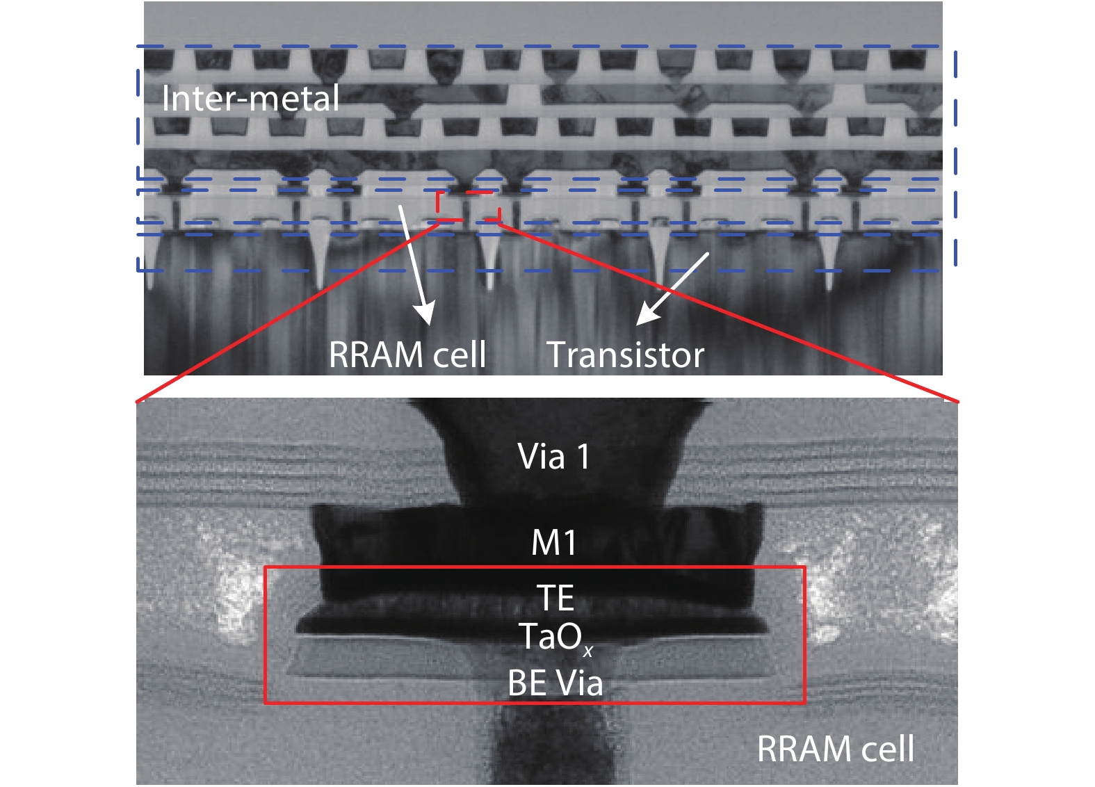
    Fig. 1. The TEM images of 1T1R RRAM cells.
    (Color online) RRAM cell basic operations: CFs forming, Reset and Set.
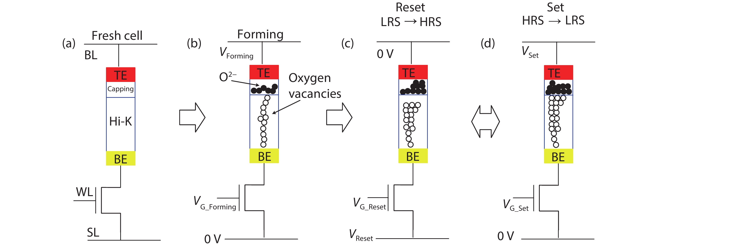
    Fig. 2. (Color online) RRAM cell basic operations: CFs forming, Reset and Set.
    (Color online) Measured I–V curve and ideal I–V curve of RRAM cell. Ideal IMP is the mid-point current of the ideal value of IHRS and ILRS. Actual IMP is the mid-point current of the measured value of IHRS and ILRS. The actual IMP is 18.4% lower than the ideal IMP.
    Fig. 3. (Color online) Measured I–V curve and ideal I–V curve of RRAM cell. Ideal IMP is the mid-point current of the ideal value of IHRS and ILRS. Actual IMP is the mid-point current of the measured value of IHRS and ILRS. The actual IMP is 18.4% lower than the ideal IMP.
    (Color online) Reference cell structure diagrams for SP scheme, PSRC scheme and HRRG scheme.
    Fig. 4. (Color online) Reference cell structure diagrams for SP scheme, PSRC scheme and HRRG scheme.
    (Color online) The distributions of cell current and the reference current.
    Fig. 5. (Color online) The distributions of cell current and the reference current.
    (Color online) The maximum latency of the CSA with different reference cells.
    Fig. 6. (Color online) The maximum latency of the CSA with different reference cells.
    (Color online) Schematic diagram of TSOCC-SA.
    Fig. 7. (Color online) Schematic diagram of TSOCC-SA.
    (Color online) The timing of TSOCC-SA.
    Fig. 8. (Color online) The timing of TSOCC-SA.
    (Color online) CSB-SA and proposed TSOCC-SA. Bit-cell state 1 (Icell > Iref) is assumed in the VA and VB waveforms.
    Fig. 9. (Color online) CSB-SA and proposed TSOCC-SA. Bit-cell state 1 (Icell > Iref) is assumed in the VA and VB waveforms.
    (Color online) (a) Simulated ∆V [= min |VA –VB|] and ∆I [= min |IA –IB|] vs. VTH mismatch between transistors M1 and M2. (b) The maximum VTH mismatch that can be tolerated by TSOCC-SA at different operation voltage.
    Fig. 10. (Color online) (a) Simulated ∆V [= min |VAVB|] and ∆I [= min |IAIB|] vs. VTH mismatch between transistors M1 and M2. (b) The maximum VTH mismatch that can be tolerated by TSOCC-SA at different operation voltage.
    (Color online) The extra area overhead and sensing margin of several offset-cancellation techniques.
    Fig. 11. (Color online) The extra area overhead and sensing margin of several offset-cancellation techniques.
    LevelFormingSetResetRead
    WLVG_Forming (1.8 V) VG_Set (1.0 V) VG_Reset (1.5 V) VDD (1.8 V)
    BLVForming (2 V) VSet (0.68 V) 0Vread (0.3 V)
    SL00VReset (1.0 V) 0
    StateLRS(RL) LRS(RL) HRS(RH) “1”/”0”
    Table 1. RRAM cell operating conditions.
    SAAreaStageTechnologyCancellation ability
    SCOC-SA [8]One Cap128 nm60%
    OCCS-SA [7]Two Caps165 nm75% or more
    CSB-SA [9]Two Caps190 nm7%
    TSOCC-SATwo Caps228 nm64%; 60%
    Table 2. Performances of several offset-cancellation techniques.
    Qiao Wang, Donglin Zhang, Yulin Zhao, Chao Liu, Xiaoxin Xu, Jianguo Yang, Hangbing Lv. Low-cost dual-stage offset-cancelled sense amplifier with hybrid read reference generator for improved read performance of RRAM at advanced technology nodes[J]. Journal of Semiconductors, 2021, 42(8): 082401
    Download Citation